EP0331334A2 - Connecteur optique - Google Patents
Connecteur optique Download PDFInfo
- Publication number
- EP0331334A2 EP0331334A2 EP89301713A EP89301713A EP0331334A2 EP 0331334 A2 EP0331334 A2 EP 0331334A2 EP 89301713 A EP89301713 A EP 89301713A EP 89301713 A EP89301713 A EP 89301713A EP 0331334 A2 EP0331334 A2 EP 0331334A2
- Authority
- EP
- European Patent Office
- Prior art keywords
- block
- groove
- grooves
- major surface
- beveled
- Prior art date
- Legal status (The legal status is an assumption and is not a legal conclusion. Google has not performed a legal analysis and makes no representation as to the accuracy of the status listed.)
- Granted
Links
Images


Classifications
-
- G—PHYSICS
- G02—OPTICS
- G02B—OPTICAL ELEMENTS, SYSTEMS OR APPARATUS
- G02B6/00—Light guides; Structural details of arrangements comprising light guides and other optical elements, e.g. couplings
- G02B6/24—Coupling light guides
-
- G—PHYSICS
- G02—OPTICS
- G02B—OPTICAL ELEMENTS, SYSTEMS OR APPARATUS
- G02B6/00—Light guides; Structural details of arrangements comprising light guides and other optical elements, e.g. couplings
- G02B6/24—Coupling light guides
- G02B6/42—Coupling light guides with opto-electronic elements
- G02B6/4292—Coupling light guides with opto-electronic elements the light guide being disconnectable from the opto-electronic element, e.g. mutually self aligning arrangements
-
- G—PHYSICS
- G02—OPTICS
- G02B—OPTICAL ELEMENTS, SYSTEMS OR APPARATUS
- G02B6/00—Light guides; Structural details of arrangements comprising light guides and other optical elements, e.g. couplings
- G02B6/24—Coupling light guides
- G02B6/26—Optical coupling means
- G02B6/30—Optical coupling means for use between fibre and thin-film device
-
- G—PHYSICS
- G02—OPTICS
- G02B—OPTICAL ELEMENTS, SYSTEMS OR APPARATUS
- G02B6/00—Light guides; Structural details of arrangements comprising light guides and other optical elements, e.g. couplings
- G02B6/24—Coupling light guides
- G02B6/36—Mechanical coupling means
- G02B6/38—Mechanical coupling means having fibre to fibre mating means
- G02B6/3807—Dismountable connectors, i.e. comprising plugs
- G02B6/3833—Details of mounting fibres in ferrules; Assembly methods; Manufacture
- G02B6/3834—Means for centering or aligning the light guide within the ferrule
- G02B6/3838—Means for centering or aligning the light guide within the ferrule using grooves for light guides
- G02B6/3839—Means for centering or aligning the light guide within the ferrule using grooves for light guides for a plurality of light guides
-
- G—PHYSICS
- G02—OPTICS
- G02B—OPTICAL ELEMENTS, SYSTEMS OR APPARATUS
- G02B6/00—Light guides; Structural details of arrangements comprising light guides and other optical elements, e.g. couplings
- G02B6/24—Coupling light guides
- G02B6/36—Mechanical coupling means
- G02B6/38—Mechanical coupling means having fibre to fibre mating means
- G02B6/3807—Dismountable connectors, i.e. comprising plugs
- G02B6/3873—Connectors using guide surfaces for aligning ferrule ends, e.g. tubes, sleeves, V-grooves, rods, pins, balls
- G02B6/3882—Connectors using guide surfaces for aligning ferrule ends, e.g. tubes, sleeves, V-grooves, rods, pins, balls using rods, pins or balls to align a pair of ferrule ends
-
- G—PHYSICS
- G02—OPTICS
- G02B—OPTICAL ELEMENTS, SYSTEMS OR APPARATUS
- G02B6/00—Light guides; Structural details of arrangements comprising light guides and other optical elements, e.g. couplings
- G02B6/24—Coupling light guides
- G02B6/36—Mechanical coupling means
- G02B6/38—Mechanical coupling means having fibre to fibre mating means
- G02B6/3807—Dismountable connectors, i.e. comprising plugs
- G02B6/3873—Connectors using guide surfaces for aligning ferrule ends, e.g. tubes, sleeves, V-grooves, rods, pins, balls
- G02B6/3885—Multicore or multichannel optical connectors, i.e. one single ferrule containing more than one fibre, e.g. ribbon type
-
- G—PHYSICS
- G02—OPTICS
- G02B—OPTICAL ELEMENTS, SYSTEMS OR APPARATUS
- G02B6/00—Light guides; Structural details of arrangements comprising light guides and other optical elements, e.g. couplings
- G02B6/24—Coupling light guides
- G02B6/36—Mechanical coupling means
- G02B6/38—Mechanical coupling means having fibre to fibre mating means
- G02B6/3807—Dismountable connectors, i.e. comprising plugs
- G02B6/389—Dismountable connectors, i.e. comprising plugs characterised by the method of fastening connecting plugs and sockets, e.g. screw- or nut-lock, snap-in, bayonet type
-
- G—PHYSICS
- G02—OPTICS
- G02B—OPTICAL ELEMENTS, SYSTEMS OR APPARATUS
- G02B6/00—Light guides; Structural details of arrangements comprising light guides and other optical elements, e.g. couplings
- G02B6/24—Coupling light guides
- G02B6/42—Coupling light guides with opto-electronic elements
- G02B6/4201—Packages, e.g. shape, construction, internal or external details
- G02B6/4204—Packages, e.g. shape, construction, internal or external details the coupling comprising intermediate optical elements, e.g. lenses, holograms
- G02B6/421—Packages, e.g. shape, construction, internal or external details the coupling comprising intermediate optical elements, e.g. lenses, holograms the intermediate optical component consisting of a short length of fibre, e.g. fibre stub
-
- G—PHYSICS
- G02—OPTICS
- G02B—OPTICAL ELEMENTS, SYSTEMS OR APPARATUS
- G02B6/00—Light guides; Structural details of arrangements comprising light guides and other optical elements, e.g. couplings
- G02B6/24—Coupling light guides
- G02B6/36—Mechanical coupling means
- G02B6/3628—Mechanical coupling means for mounting fibres to supporting carriers
- G02B6/3632—Mechanical coupling means for mounting fibres to supporting carriers characterised by the cross-sectional shape of the mechanical coupling means
- G02B6/3636—Mechanical coupling means for mounting fibres to supporting carriers characterised by the cross-sectional shape of the mechanical coupling means the mechanical coupling means being grooves
-
- G—PHYSICS
- G02—OPTICS
- G02B—OPTICAL ELEMENTS, SYSTEMS OR APPARATUS
- G02B6/00—Light guides; Structural details of arrangements comprising light guides and other optical elements, e.g. couplings
- G02B6/24—Coupling light guides
- G02B6/36—Mechanical coupling means
- G02B6/3628—Mechanical coupling means for mounting fibres to supporting carriers
- G02B6/3648—Supporting carriers of a microbench type, i.e. with micromachined additional mechanical structures
- G02B6/3652—Supporting carriers of a microbench type, i.e. with micromachined additional mechanical structures the additional structures being prepositioning mounting areas, allowing only movement in one dimension, e.g. grooves, trenches or vias in the microbench surface, i.e. self aligning supporting carriers
-
- G—PHYSICS
- G02—OPTICS
- G02B—OPTICAL ELEMENTS, SYSTEMS OR APPARATUS
- G02B6/00—Light guides; Structural details of arrangements comprising light guides and other optical elements, e.g. couplings
- G02B6/24—Coupling light guides
- G02B6/36—Mechanical coupling means
- G02B6/3628—Mechanical coupling means for mounting fibres to supporting carriers
- G02B6/3684—Mechanical coupling means for mounting fibres to supporting carriers characterised by the manufacturing process of surface profiling of the supporting carrier
- G02B6/3692—Mechanical coupling means for mounting fibres to supporting carriers characterised by the manufacturing process of surface profiling of the supporting carrier with surface micromachining involving etching, e.g. wet or dry etching steps
Definitions
- This invention relates to optical fiber connectors.
- a typical connector for fiber arrays comprises two plugs of silicon with grooves formed therein for accommodating the fibers.
- Each plug is formed from two mated members which are bonded together to encase the fibers.
- the grooves are formed prior to bonding by anisotropically etching a major surface of each member in an array corresponding to the fibers so that when the members are bonded, each fiber lies in a groove which is precisely aligned with all other fibers in the array.
- Another approach employs etching of deep grooves in the top and bottom surfaces of each plug and then aligning the two plugs by means of a chip extending between the two plugs and having ridges which fit within the grooves.
- etching of deep grooves in the top and bottom surfaces of each plug employs etching of deep grooves in the top and bottom surfaces of each plug and then aligning the two plugs by means of a chip extending between the two plugs and having ridges which fit within the grooves.
- U.S. Patent No. 3,864,018 issued to Miller See, e.g., U.S. Patent No. 3,864,018 issued to Miller.
- precise machining of the plug surfaces is expensive.
- a still further approach employs grooves which are machined on the edges of the plugs and utilizes alignment pins pressed into the grooves by spring clips to bridge the gap between plugs (see, C. M. Miller, "Optical Fiber Splices and Connectors", pp. 336-338). Again, the alignment grooves have
- the connector comprises a block of material with edge and major surfaces.
- the block includes at least one groove with sloping sidewalls formed in a major surface and adapted to receive an optical fiber.
- the block also includes a beveled portion extending from the major surface on each edge surface such that the slope of each beveled portion is the same as one of the sidewalls of the groove.
- a spline is disposed in contact with the beveled portion of at least one edge surface, extends beyond the plug, and is adapted for engagement with the beveled portion of a similar plug for alignment therewith. Means are also included for maintaining the spline in contact with the beveled portion.
- the invention is a method of forming an optical fiber connector from a block material having major surfaces.
- a first groove is formed in a major surface of the block and is adapted for receiving an optical fiber therein.
- a pair of grooves is also formed in the major surface, one on either side of the first groove and essentially parallel therewith. The pair of grooves are deeper than the first groove and are formed essentially simultaneously with the first groove.
- the block of material is cut through a bottom portion of the pair of grooves and along a line essentially parallel with the first groove thereby forming edge surfaces including beveled portions extending from the major surface of the block which includes the first groove.
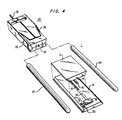
- Each half connector e.g., 1
- Each half connector includes two blocks 10 and 11, of a material with facing major surfaces 12 and 13, respectively.
- the plugs are desirably made from a crystal material such as silicon, for reasons which will become clearer.
- Each major surface has an array of grooves, e.g., 14 and 15, etched therein.
- the grooves are of a size and shape so that when the two blocks are bonded together, corresponding grooves in each surface will accommodate an optical fiber, e.g., 16, from an array of fibers to be connected (see FIG. 2).
- Each fiber will make contact with the sloped surfaces of the two corresponding grooves from the blocks as shown.
- a crystal for the block material permits taking advantage of certain crystal planes to precisely form the groove surfaces.
- a silicon block with a major surface in the (100) crystallographic plane will be etched anisotropically to form grooves with surfaces lying in the (111) planes. Therefore, the angle of the two sloping walls of a groove will always be precisely determined by the orientation of the crystal planes (in this example, approximately 55°) with respect to the major structure regardless of the time of etching the major surface.
- the size of the opening will therefore primarily be determined by the size of the openings in the etch mask.
- grooves are shown with a "V" configuration, it is also possible to achieve grooves with a flat bottom by stopping the etching short of a complete etching of the crystal planes. However, sloping sidewalls with the same orientation will still be produced.
- alignment between the fiber arrays is provided by forming beveled portions (17, 18, 19 and 20) on each edge surface of each block 10 and 11 (the beveled surfaces are similarly formed on the blocks of plug 30).
- the beveled portions extend from the major surfaces (12 and 13) of each block and have the same slope as the groove surfaces.
- Each block, such as 10, is formed from a larger silicon wafer 40.
- a standard mask material, 41 such as thermally grown SiO 2 deposited over the major surface of the wafer which is the (100) crystallographic plane.
- the mask openings are formed by standard photolithographic techniques to expose the areas of silicon where the fiber grooves will be etched. Wider mask openings are also formed over the silicon areas adjacent to the fiber grooves (one on each side of the array). Typically, the openings for etching the fiber grooves are approximately 140 ⁇ m wide, while the openings for etching the larger grooves are approximately 1000 ⁇ m wide.
- a standard anisotropic etchant is then applied to the structure to form the fiber grooves (e.g., 14) and deeper grooves 21 and 22 adjacent thereto.
- the deeper grooves include side walls, e.g., 18 and 20, which have the same slope as the fiber grooves since they are formed by the same anisotropic etch along the same crystal planes (the (111) plane).
- the fiber grooves would be typically approximately 98 ⁇ m deep while the adjacent grooves (21 and 22) would be approximately 500 ⁇ m deep.
- etchants such as ethylene diamine pyrocatechol (EDP)
- EDP ethylene diamine pyrocatechol
- An etchant which tends to undercut the mask such as KOH can still be used in a single step if the mask openings over the fiber groove area are made sufficiently narrow to take this undercutting into account.
- the two sets of grooves can be formed in two etching steps. For the first step, mask openings would be formed only over the area of the deeper grooves and those areas would be etched to a predetermined depth short of the desired depth for those grooves. Openings in the mask would be made over the area comprising the fiber grooves, and these fiber grooves would then be etched to their desired depth while the etching of the deeper grooves would be completed.
- the mask is stripped off.
- the wafer is then cut into individual blocks by sawing through the etched surfaces of the deeper grooves 21 and 22 along lines illustrated as 42 and 43.
- the saw lines extend substantially the entire length of the deeper grooves (into the plane illustrated in FIG. 3) and substantially parallel to the longitudinal dimension of the fiber grooves.
- a plurality of blocks such as 10 of FIGs 1 and 2 are produced with beveled surfaces (e.g., 18 and 20) formed from one wall of the deep grooves on either side of the fiber grooves.
- the plugs also include ledge portions, 23 and 24, of FIG. 2 formed from part of the bottom surface of the deep grooves. These ledge portions can remain as shown or can be removed if desired.
- the blocks are assembled by placing each fiber of the array within its corresponding groove and mating the two blocks 10 and 11 to form the appropriate housing for each fiber (FIG. 2).
- the two major surfaces are bonded together by standard means such as epoxy.
- each rod is held in contact with the beveled portions 17, 18, 19 and 20 of a corresponding edge surface of the plug 1.
- the rods also extend beyond the front surface of the plugs so that each rod can be slid into contact with the beveled portions of the edge surfaces of the other plug 30.
- the splines as shown are in the form of rods which are cylindrical in shape but can be tapered at one end for easy insertion. However, the splines can be any member bridging the gap between plugs which can be held in contact with and align the beveled portions.
- the rods, 25 and 26, are spring loaded to maintain intimate contact with the beveled portions.
- the spring force is provided by means including a clip portion 27 extending around the two plugs (except for a narrow gap). Extending from the clip are a pair of prongs 28 and 29, each adjacent to a corresponding edge surface of the assembled plug but maintaining a slight gap therewith which is smaller than the diameter of the rods. The rods are inserted in this gap and held against the beveled portions of the edge surfaces by the spring force created by the prongs 28 and 29. This force tends to pull the blocks apart but for the presence of the clip portion.
- the center axes (32 and 33 of FIG. 2) of the rods will be in line with all the center axes (e.g., 34) of the fibers. That is, the rods and fibers are rectilinear. This will be the case regardless of any overetching or underetching of the two blocks 10 and 11 during the formation of the grooves since any shift in the position of the fibers relative to the major surfaces of the blocks will be experienced to the same extent by the guiding rods.
- the guiding rods are inserted within the gaps formed between the prongs 35 and 36 and the beveled portions (not shown) of the edge surfaces of the blocks of the other plug 30 until the front faces of the plugs are in physical contact.
- the spring means of the two plugs are typically identical.
- the rods 25 and 26 are, therefore, pressed into intimate contact with the beveled surfaces of both plugs 1 and 30.
- rods are rectilinear with the fibers of the plug 1 as discussed previously, and the beveled portions of the other plug 30 are also formed at the same slope as the fiber grooves of that plug, it follows that when rods 25 and 26 are pressed against the beveled portions of plug 30 they will also be rectilinear with the fibers of that plug and that the two fiber arrays will be in complete alignment. This will be the case regardless of the amount of overetch or underetch of the silicon blocks forming either plug. It will be appreciated that, although two guiding rods, 25 and 26, are shown as attached to one plug (1), if desired, one rod could be attached to one of the edge surfaces of each plug 1 and 30, prior to mating.
- the plug 1 can be formed as before but with one of the silicon blocks 10 being extended so that a semiconductor laser 50 can be formed on the major surface along with contacts 51 and 52 and a waveguide 53.
- a semiconductor laser 50 can be formed on the major surface along with contacts 51 and 52 and a waveguide 53.
- other types of components such as receivers, can be formed on the surface.
- the other plug, 30, can be formed as before, but this time enclosing a single fiber 32, and retaining the rods 25 and 26.
- the fiber, 32 will meet a fiber, 16, preinserted within the groove formed by the two silicon blocks 10 and 11 of plug 1 which latter-fiber is in contact with the waveguide 53 formed up to the edge of the groove.
- the rods will be held against the beveled portions of plugs 1 and 30 by the prongs 35 and 36 of plug 30 (i.e., no spring is needed around blocks 10 and 11.
- connection between the fiber 32 and laser 50 is established with a close alignment.
- a plurality of fibers within each plug may also be connected with this type of arrangement.
Landscapes
- Physics & Mathematics (AREA)
- General Physics & Mathematics (AREA)
- Optics & Photonics (AREA)
- Mechanical Coupling Of Light Guides (AREA)
- Optical Couplings Of Light Guides (AREA)
Applications Claiming Priority (2)
| Application Number | Priority Date | Filing Date | Title |
|---|---|---|---|
| US07163690 US4818058B1 (en) | 1988-03-03 | 1988-03-03 | Optical connector. |
| US163690 | 1988-03-03 |
Publications (3)
| Publication Number | Publication Date |
|---|---|
| EP0331334A2 true EP0331334A2 (fr) | 1989-09-06 |
| EP0331334A3 EP0331334A3 (fr) | 1991-01-16 |
| EP0331334B1 EP0331334B1 (fr) | 1995-04-26 |
Family
ID=22591157
Family Applications (1)
| Application Number | Title | Priority Date | Filing Date |
|---|---|---|---|
| EP89301713A Expired - Lifetime EP0331334B1 (fr) | 1988-03-03 | 1989-02-22 | Connecteur optique |
Country Status (8)
| Country | Link |
|---|---|
| US (1) | US4818058B1 (fr) |
| EP (1) | EP0331334B1 (fr) |
| JP (1) | JP2551988B2 (fr) |
| KR (1) | KR0172594B1 (fr) |
| CA (1) | CA1314161C (fr) |
| DE (1) | DE68922332T2 (fr) |
| ES (1) | ES2071655T3 (fr) |
| HK (1) | HK100196A (fr) |
Cited By (14)
| Publication number | Priority date | Publication date | Assignee | Title |
|---|---|---|---|---|
| WO1992000538A1 (fr) * | 1990-07-02 | 1992-01-09 | British Telecommunications Public Limited Company | Systeme optique |
| WO1992006394A1 (fr) * | 1990-10-09 | 1992-04-16 | British Telecommunications Public Limited Company | Guides d'ondes et rainures en v a alignement automatique |
| EP0508678A3 (fr) * | 1991-04-12 | 1992-12-30 | AT&T Corp. | Article pour connecter des fibres optiques |
| EP0529947A1 (fr) * | 1991-08-30 | 1993-03-03 | AT&T Corp. | Ensemble optique avec un dispositif de fixation de fibre |
| EP0611142A1 (fr) * | 1993-02-12 | 1994-08-17 | Ngk Insulators, Ltd. | Procédé pour compler optiquement une matrice de fibres optiques avec un membre opposant |
| EP0618468A1 (fr) * | 1993-03-29 | 1994-10-05 | Motorola, Inc. | Interface pour coupler des fibres optiques à des circuits électroniques |
| EP0629888A3 (fr) * | 1993-06-18 | 1995-01-18 | Sel Alcatel Ag | |
| EP0636911A1 (fr) * | 1993-07-27 | 1995-02-01 | Nec Corporation | Structure de couplage entre semi-conducteur optique et guide d'onde optique, et méthode de couplage |
| US5656120A (en) * | 1994-07-28 | 1997-08-12 | Ngk Insulators, Ltd. | Method of fixing optical fiber array to substrate |
| FR2749406A1 (fr) * | 1996-06-04 | 1997-12-05 | Laniepce Sylvie | Dispositif de transition de pas, notamment pour fibres optiques |
| US5835659A (en) * | 1995-02-21 | 1998-11-10 | Ngk Insulators, Ltd. | Optical fiber-fixing substrate, method of producing the same and optical device |
| US6027253A (en) * | 1995-08-24 | 2000-02-22 | Ngk Insulators, Ltd. | Optical fiber array |
| WO2000041017A1 (fr) * | 1999-01-07 | 2000-07-13 | Nu-Wave Photonics Inc. | Fibres optiques sans adhesif pour boitier de guides d'ondes optiques |
| WO2000042461A1 (fr) * | 1999-01-11 | 2000-07-20 | Nu-Wave Photonics Inc. | Procede de fabrication de dispositifs optiques integres connectes a des fibres optiques et dispositifs ainsi obtenus |
Families Citing this family (79)
| Publication number | Priority date | Publication date | Assignee | Title |
|---|---|---|---|---|
| US4973127A (en) * | 1989-05-31 | 1990-11-27 | At&T Bell Laboratories | Multifiber optical connector and method of making same |
| JP2590266B2 (ja) * | 1989-06-23 | 1997-03-12 | 住友電気工業株式会社 | 光コネクタ |
| GB8917226D0 (en) * | 1989-07-27 | 1989-09-13 | British Telecomm | Multifibre connectorisation |
| US5005941A (en) * | 1989-09-05 | 1991-04-09 | Gte Products Corporation | Fiber optic splice assembly |
| IT1231076B (it) * | 1989-09-28 | 1991-11-12 | Pirelli Cavi Spa | Procedimento per la realizzazione di gruppo di connessione separabile per fibre ottiche riunite a nastro e gruppo di connessione con esso realizzato. |
| FR2652912B1 (fr) * | 1989-10-09 | 1994-02-25 | Corning Glass Works | Procede d'encapsulage d'un composant optique d'interconnexion de fibres optiques, composant encapsule obtenu par la mise en óoeuvre de ce procede et enveloppe formant partie de ce composant. |
| JPH0650362B2 (ja) * | 1989-10-17 | 1994-06-29 | 住友電気工業株式会社 | 光ファイバ配列部材及びその形成方法 |
| US4998796A (en) * | 1990-02-27 | 1991-03-12 | At&T Bell Laboratories | Method of assembling multi-grooved silicon chip fiber optic terminations |
| US5082346A (en) * | 1990-06-28 | 1992-01-21 | At&T Bell Laboratories | Field-assemblable multifiber optical connector |
| US5121456A (en) * | 1990-09-06 | 1992-06-09 | Reliance Comm/Tec Corporation | Polymer spring fiber optic splicer, tool for operating same and panel incorporating same |
| GB9021956D0 (en) * | 1990-10-09 | 1990-11-21 | British Telecomm | Optical fibre connector |
| US5155785A (en) * | 1991-05-01 | 1992-10-13 | At&T Bell Laboratories | Optical fiber interconnection apparatus and method |
| AU649162B2 (en) * | 1991-08-17 | 1994-05-12 | Nippon Telegraph & Telephone Corporation | Optical connector |
| US5151964A (en) * | 1991-09-06 | 1992-09-29 | Minnesota Mining And Manufacturing Company | Wedge-actuated multiple optical fiber splice |
| US5204925A (en) * | 1991-09-11 | 1993-04-20 | At&T Bell Laboratories | Optical interconnection of circuit packs |
| US5315678A (en) * | 1992-03-30 | 1994-05-24 | Nippon Telegraph & Telephone Corporation | Optical fiber connector |
| US5257332A (en) * | 1992-09-04 | 1993-10-26 | At&T Bell Laboratories | Optical fiber expanded beam coupler |
| FR2695733B1 (fr) * | 1992-09-11 | 1994-11-04 | Mars Actel | Procédés de préparation du raccordement par épissurage d'un dispositif d'optique intégrée à au moins un câble optique. |
| JPH06138345A (ja) * | 1992-10-27 | 1994-05-20 | Seiko Giken:Kk | 光ファイバスプライサ |
| US5268981A (en) * | 1992-11-16 | 1993-12-07 | At&T Bell Laboratories | Optical fiber connector methods using a substrate with an aperture |
| US5388174A (en) * | 1993-02-22 | 1995-02-07 | At&T Corp. | Optical fiber connector techniques |
| US5287426A (en) | 1993-02-22 | 1994-02-15 | At&T Bell Laboratories | Methods for making optical fiber connectors |
| KR100225026B1 (ko) * | 1993-03-31 | 1999-10-15 | 구라우치 노리타카 | 광파이버어레이 |
| EP0631162B1 (fr) * | 1993-06-25 | 1998-09-09 | AT&T Corp. | Procédé de liaison de fibres optiques |
| US5345323A (en) * | 1993-08-02 | 1994-09-06 | At&T Bell Laboratories | Techniques for polishing optical fiber ends |
| US5333225A (en) * | 1993-08-03 | 1994-07-26 | International Business Machines Corporation | Substrate-embedded pluggable receptacles for connecting clustered optical cables to a module |
| US5392373A (en) * | 1993-11-29 | 1995-02-21 | The Whitaker Corporation | Apparatus for optically coupling an optical fiber to an electro-optic device |
| US5430819A (en) * | 1993-12-21 | 1995-07-04 | At&T Corp. | Multiple optical fiber connector and method of making same |
| US5440657A (en) * | 1994-05-26 | 1995-08-08 | The Whitaker Corporation | Re-enterable splicer for ribbon fiber |
| US5550942A (en) * | 1994-07-18 | 1996-08-27 | Sheem; Sang K. | Micromachined holes for optical fiber connection |
| US5633968A (en) * | 1994-07-18 | 1997-05-27 | Sheem; Sang K. | Face-lock interconnection means for optical fibers and other optical components and manufacturing methods of the same |
| CA2194986A1 (fr) * | 1994-07-18 | 1996-02-01 | Sang K. Sheem | Moyens d'interconnexion a verrouillage face contre face, pour fibres optiques et pour autres composants optiques, et procedes de fabrication correspondants |
| US5468338A (en) * | 1994-07-22 | 1995-11-21 | At&T Ipm Corp. | Methods for selectively wet etching substrates |
| US5519798A (en) * | 1994-08-15 | 1996-05-21 | At&T Corp. | Optical fiber connector including V-groove/pin alignment means |
| US5483611A (en) * | 1994-08-26 | 1996-01-09 | At&T Corp. | Apparatus for aligning optical fibers in an X-Y matrix configuration |
| US5513294A (en) * | 1994-12-08 | 1996-04-30 | At&T Corp. | Method of forming optical fiber connectors |
| US5632908A (en) * | 1995-02-01 | 1997-05-27 | Lucent Technologies Inc. | Method for making aligned features |
| US6004042A (en) * | 1995-07-28 | 1999-12-21 | Berg Technology, Inc. | Multi-fiber connector |
| US5620634A (en) * | 1995-08-17 | 1997-04-15 | Lucent Technologies Inc. | Method of making fiber waveguide connectors |
| US5687263A (en) * | 1995-10-02 | 1997-11-11 | The United States Of America As Represented By The Secretary Of The Navy | Optical RF bandpass filter and method for manufacturing same |
| KR0184963B1 (ko) * | 1995-10-31 | 1999-05-15 | 유기범 | 다심 광 케이블 접속용 콘넥터 조립체 |
| DE19547525C1 (de) * | 1995-12-08 | 1997-02-20 | Siemens Ag | Lösbarer Stecker |
| US6045270A (en) | 1995-12-22 | 2000-04-04 | Methode Electronics, Inc. | Massive parallel optical interconnect system |
| US5737463A (en) * | 1995-12-22 | 1998-04-07 | Weiss; Roger E. | Massive parallel optical interconnect system |
| JP3198039B2 (ja) | 1996-01-12 | 2001-08-13 | 日立電線株式会社 | 光ファイバアレイ部品及びその製造方法 |
| US5703973A (en) * | 1996-03-29 | 1997-12-30 | Lucent Technologies Inc. | Optical integrated circuit having passively aligned fibers and method using same |
| KR19980016218A (ko) * | 1996-08-27 | 1998-05-25 | 양승택 | 다심 광커넥터 |
| US6168317B1 (en) | 1998-04-30 | 2001-01-02 | Lucent Technologies Inc. | Alignment adapter for an optical connector and method for making same |
| US6096229A (en) * | 1998-07-30 | 2000-08-01 | Lucent Technologies Inc. | Method of making alignment grooves in an optical connector support member |
| US6276841B1 (en) | 1999-10-20 | 2001-08-21 | Berg Technology, Inc. | Connector with low-profile latch |
| US7167615B1 (en) | 1999-11-05 | 2007-01-23 | Board Of Regents, The University Of Texas System | Resonant waveguide-grating filters and sensors and methods for making and using same |
| US6386767B1 (en) | 1999-12-30 | 2002-05-14 | Fci Americas Technology, Inc. | High density multiple chip fiber array connector |
| US6210047B1 (en) | 2000-02-04 | 2001-04-03 | Molex Incorporated | Method of fabricating a fiber optic connector ferrule |
| US6447171B1 (en) | 2000-02-04 | 2002-09-10 | Fci Americas Technology, Inc | Multi-fiber array connector system |
| US6422761B1 (en) | 2000-03-06 | 2002-07-23 | Fci Americas Technology, Inc. | Angled optical connector |
| US6474878B1 (en) | 2000-03-28 | 2002-11-05 | Berg Technology, Inc. | Optical connector |
| US6847764B2 (en) * | 2000-04-14 | 2005-01-25 | Shipley Company, L.L.C. | Optical interconnect having alignment depression |
| US6450697B1 (en) | 2000-08-24 | 2002-09-17 | Berg Technology, Inc. | Optical connector having a combined guide pin lock and grounding contact |
| US6464407B1 (en) | 2000-10-13 | 2002-10-15 | Berg Technology, Inc. | Optical connector having a ferrule with alignment and sealing features |
| US7345316B2 (en) * | 2000-10-25 | 2008-03-18 | Shipley Company, L.L.C. | Wafer level packaging for optoelectronic devices |
| US6932519B2 (en) | 2000-11-16 | 2005-08-23 | Shipley Company, L.L.C. | Optical device package |
| US6799897B2 (en) | 2000-11-16 | 2004-10-05 | Shipley Company, L.L.C. | Optical connector system |
| US6883977B2 (en) * | 2000-12-14 | 2005-04-26 | Shipley Company, L.L.C. | Optical device package for flip-chip mounting |
| US6491553B2 (en) | 2000-12-20 | 2002-12-10 | Berg Technology, Inc. | Electrical connector having an electrical contact with a formed solder cup |
| US6550980B2 (en) * | 2001-04-05 | 2003-04-22 | Stratos Lightwave, Inc. | Optical ferrule having multiple rows of multiple optical fibers |
| US6695488B2 (en) * | 2001-07-19 | 2004-02-24 | Cinch Connectors, Inc. | Tool and method for forming a multi fiber ferrule |
| US6736546B2 (en) * | 2001-08-31 | 2004-05-18 | Teradyne, Inc. | Optical connector ferrule designed to minimize manufacturing imperfections and mating misalignments by incorporating exact constraint principles |
| CN1302307C (zh) * | 2001-11-08 | 2007-02-28 | 希普雷公司 | 光纤终端 |
| US20030174998A1 (en) * | 2002-03-15 | 2003-09-18 | George Shevchuk | Assembly for stacking optical fibers in an aligned two dimensional array |
| US6874950B2 (en) * | 2002-12-17 | 2005-04-05 | International Business Machines Corporation | Devices and methods for side-coupling optical fibers to optoelectronic components |
| US6817777B1 (en) | 2003-06-27 | 2004-11-16 | Dimitry Grabbe | Fiber array ferrule |
| US6816654B1 (en) * | 2003-06-27 | 2004-11-09 | Dimitry Grabbe | Fiber array ferrule and method of making |
| US6961489B2 (en) * | 2003-06-30 | 2005-11-01 | Finisar Corporation | High speed optical system |
| US7149383B2 (en) * | 2003-06-30 | 2006-12-12 | Finisar Corporation | Optical system with reduced back reflection |
| US20110224554A1 (en) * | 2010-03-12 | 2011-09-15 | Optomak Inc. | Optogenetic Fiber Optic Cannula and Adapted Fiber Optic Connector |
| JP6334510B2 (ja) * | 2012-04-05 | 2018-05-30 | ナノプレシジョン プロダクツ インコーポレイテッドNanoprecision Products, Inc. | 位置合わせピンをクランプ留めするための対応構造を有する、光ファイバコネクタ用のフェルール |
| EP3593186A1 (fr) * | 2017-03-07 | 2020-01-15 | Corning Optical Communications LLC | Adaptateur photonique universel pour coupler un connecteur optique à un substrat optoélectronique |
| WO2020235041A1 (fr) * | 2019-05-22 | 2020-11-26 | 日本電信電話株式会社 | Structure de connexion de guide d'ondes, puce de guide d'ondes, connecteur, procédé de fabrication de composant de connexion de guide d'ondes, et procédé de connexion de gude d'ondes |
| WO2021120669A1 (fr) * | 2019-12-20 | 2021-06-24 | 青岛海信宽带多媒体技术有限公司 | Module optique |
Family Cites Families (11)
| Publication number | Priority date | Publication date | Assignee | Title |
|---|---|---|---|---|
| US3864018A (en) * | 1973-10-18 | 1975-02-04 | Bell Telephone Labor Inc | Method and means for splicing arrays of optical fibers |
| JPS5426030Y2 (fr) * | 1975-08-28 | 1979-08-29 | ||
| GB1600272A (en) * | 1977-05-02 | 1981-10-14 | Plessey Co Ltd | Optical fibre connectors |
| JPS5932766B2 (ja) * | 1980-09-25 | 1984-08-10 | 富士通株式会社 | 光コネクタの位置出し構造 |
| JPS57158824A (en) * | 1981-03-27 | 1982-09-30 | Nippon Sheet Glass Co Ltd | Optical connector |
| JPS57202506A (en) * | 1981-06-06 | 1982-12-11 | Nippon Sheet Glass Co Ltd | Optical circuit and its production |
| US4475790A (en) * | 1982-01-25 | 1984-10-09 | Spire Corporation | Fiber optic coupler |
| US4515434A (en) * | 1983-03-09 | 1985-05-07 | Allied Corporation | Fiber optic connector |
| JPS6161111A (ja) * | 1984-09-01 | 1986-03-28 | Sumitomo Electric Ind Ltd | 多心光コネクタ |
| US4725114A (en) * | 1984-09-28 | 1988-02-16 | American Telephone And Telegraph Company, At&T Bell Laboratories | Optical waveguide lateral alignment arrangement |
| US4725120A (en) * | 1984-10-25 | 1988-02-16 | American Telephone And Telegraph Company, At&T Bell Laboratories | Connector apparatus |
-
1988
- 1988-03-03 US US07163690 patent/US4818058B1/en not_active Expired - Lifetime
-
1989
- 1989-01-10 JP JP1002158A patent/JP2551988B2/ja not_active Expired - Fee Related
- 1989-02-22 EP EP89301713A patent/EP0331334B1/fr not_active Expired - Lifetime
- 1989-02-22 DE DE68922332T patent/DE68922332T2/de not_active Expired - Fee Related
- 1989-02-22 ES ES89301713T patent/ES2071655T3/es not_active Expired - Lifetime
- 1989-02-28 KR KR1019890002387A patent/KR0172594B1/ko not_active Expired - Fee Related
- 1989-02-28 CA CA000592336A patent/CA1314161C/fr not_active Expired - Fee Related
-
1996
- 1996-06-06 HK HK100196A patent/HK100196A/en not_active IP Right Cessation
Cited By (21)
| Publication number | Priority date | Publication date | Assignee | Title |
|---|---|---|---|---|
| AU642512B2 (en) * | 1990-07-02 | 1993-10-21 | British Telecommunications Public Limited Company | Optical system |
| US5371820A (en) * | 1990-07-02 | 1994-12-06 | British Telecommunications Public Limited Company | Optical hybrid motherboard interconnection system and method of assembling same |
| WO1992000538A1 (fr) * | 1990-07-02 | 1992-01-09 | British Telecommunications Public Limited Company | Systeme optique |
| WO1992006394A1 (fr) * | 1990-10-09 | 1992-04-16 | British Telecommunications Public Limited Company | Guides d'ondes et rainures en v a alignement automatique |
| US5342478A (en) * | 1990-10-09 | 1994-08-30 | British Telecommunications Public Limited Company | Self-aligned V-grooves and waveguides |
| EP0508678A3 (fr) * | 1991-04-12 | 1992-12-30 | AT&T Corp. | Article pour connecter des fibres optiques |
| EP0529947A1 (fr) * | 1991-08-30 | 1993-03-03 | AT&T Corp. | Ensemble optique avec un dispositif de fixation de fibre |
| US5482585A (en) * | 1993-02-12 | 1996-01-09 | Ngk Insulators, Ltd. | Process for optically joining an optical fiber array to an opponent member |
| EP0611142A1 (fr) * | 1993-02-12 | 1994-08-17 | Ngk Insulators, Ltd. | Procédé pour compler optiquement une matrice de fibres optiques avec un membre opposant |
| EP0618468A1 (fr) * | 1993-03-29 | 1994-10-05 | Motorola, Inc. | Interface pour coupler des fibres optiques à des circuits électroniques |
| US5818994A (en) * | 1993-06-18 | 1998-10-06 | Alcatel N.V. | Device for the unadjusted coupling of a number of optical waveguides to a laser array |
| EP0629888A3 (fr) * | 1993-06-18 | 1995-01-18 | Sel Alcatel Ag | |
| US5414787A (en) * | 1993-07-27 | 1995-05-09 | Nec Corporation | Coupling structure between optical semiconductor and optical waveguide, and coupling method of the same |
| EP0636911A1 (fr) * | 1993-07-27 | 1995-02-01 | Nec Corporation | Structure de couplage entre semi-conducteur optique et guide d'onde optique, et méthode de couplage |
| US5656120A (en) * | 1994-07-28 | 1997-08-12 | Ngk Insulators, Ltd. | Method of fixing optical fiber array to substrate |
| US5835659A (en) * | 1995-02-21 | 1998-11-10 | Ngk Insulators, Ltd. | Optical fiber-fixing substrate, method of producing the same and optical device |
| US5991492A (en) * | 1995-02-21 | 1999-11-23 | Ngk Insulators, Ltd. | Optical fiber-fixing substrate, method of producing the same and optical device |
| US6027253A (en) * | 1995-08-24 | 2000-02-22 | Ngk Insulators, Ltd. | Optical fiber array |
| FR2749406A1 (fr) * | 1996-06-04 | 1997-12-05 | Laniepce Sylvie | Dispositif de transition de pas, notamment pour fibres optiques |
| WO2000041017A1 (fr) * | 1999-01-07 | 2000-07-13 | Nu-Wave Photonics Inc. | Fibres optiques sans adhesif pour boitier de guides d'ondes optiques |
| WO2000042461A1 (fr) * | 1999-01-11 | 2000-07-20 | Nu-Wave Photonics Inc. | Procede de fabrication de dispositifs optiques integres connectes a des fibres optiques et dispositifs ainsi obtenus |
Also Published As
| Publication number | Publication date |
|---|---|
| DE68922332T2 (de) | 1995-09-28 |
| ES2071655T3 (es) | 1995-07-01 |
| EP0331334B1 (fr) | 1995-04-26 |
| EP0331334A3 (fr) | 1991-01-16 |
| HK100196A (en) | 1996-06-14 |
| DE68922332D1 (de) | 1995-06-01 |
| KR0172594B1 (ko) | 1999-05-01 |
| JPH01229207A (ja) | 1989-09-12 |
| US4818058B1 (en) | 1995-04-25 |
| CA1314161C (fr) | 1993-03-09 |
| US4818058A (en) | 1989-04-04 |
| JP2551988B2 (ja) | 1996-11-06 |
| KR890015046A (ko) | 1989-10-28 |
Similar Documents
| Publication | Publication Date | Title |
|---|---|---|
| US4818058A (en) | Optical connector | |
| US5613024A (en) | Alignment of optical fiber arrays to optical integrated circuits | |
| US20030174998A1 (en) | Assembly for stacking optical fibers in an aligned two dimensional array | |
| EP3907540B1 (fr) | Procédé de fabrication d'un ensemble multifibre | |
| US4762387A (en) | Array connector for optical fibers | |
| US5896479A (en) | Massive parallel optical interconnect system | |
| CA1063398A (fr) | Connecteur optique pour guide d'ondes | |
| US6364539B1 (en) | Stackable multi-fiber ferrules having improved interconnection density | |
| EP1124147A2 (fr) | Coupleur à fibres optiques avec connecteur optique et procédé d'interconnexion | |
| EP1092994A2 (fr) | Connecteurs optiques à grande densité | |
| US4220397A (en) | Optical fiber connector | |
| JP2000284146A (ja) | 積層可能なマルチファイバフェルールの組立方法 | |
| US20010051026A1 (en) | Optical fiber ferrule made from dry etched parts | |
| EP1118890A2 (fr) | Connecteur à réseau de fibres optiques multiple à grande densité | |
| US6847764B2 (en) | Optical interconnect having alignment depression | |
| EP1010999A2 (fr) | Adapteurs à rainures en "V" pour l'interconnexion de guides d'ondes optiques, et procédé de leur fabrication | |
| JPH05134146A (ja) | 多芯光コネクタフエルール | |
| US20030123833A1 (en) | Embedded waveguide with alignment grooves and method for making same | |
| GB2374155A (en) | A tapered optical waveguide formed with two substrates | |
| US20040247248A1 (en) | Passive alignment between waveguides and optical components | |
| EP1363148B1 (fr) | Dispositif optique de couplage et procédé de fabrication associé | |
| IE913492A1 (en) | Optical fibre connector | |
| JP2005134903A (ja) | 光ファイバ・コネクタ、およびその製造方法 | |
| JPH068913U (ja) | 光学素子結合構造 | |
| JPH10282367A (ja) | 光コネクタ |
Legal Events
| Date | Code | Title | Description |
|---|---|---|---|
| PUAI | Public reference made under article 153(3) epc to a published international application that has entered the european phase |
Free format text: ORIGINAL CODE: 0009012 |
|
| AK | Designated contracting states |
Kind code of ref document: A2 Designated state(s): DE ES FR GB IT NL SE |
|
| PUAL | Search report despatched |
Free format text: ORIGINAL CODE: 0009013 |
|
| AK | Designated contracting states |
Kind code of ref document: A3 Designated state(s): DE ES FR GB IT NL SE |
|
| 17P | Request for examination filed |
Effective date: 19910708 |
|
| 17Q | First examination report despatched |
Effective date: 19921012 |
|
| RAP3 | Party data changed (applicant data changed or rights of an application transferred) |
Owner name: AT&T CORP. |
|
| GRAA | (expected) grant |
Free format text: ORIGINAL CODE: 0009210 |
|
| AK | Designated contracting states |
Kind code of ref document: B1 Designated state(s): DE ES FR GB IT NL SE |
|
| ITF | It: translation for a ep patent filed | ||
| ET | Fr: translation filed | ||
| REF | Corresponds to: |
Ref document number: 68922332 Country of ref document: DE Date of ref document: 19950601 |
|
| REG | Reference to a national code |
Ref country code: ES Ref legal event code: FG2A Ref document number: 2071655 Country of ref document: ES Kind code of ref document: T3 |
|
| PLBE | No opposition filed within time limit |
Free format text: ORIGINAL CODE: 0009261 |
|
| STAA | Information on the status of an ep patent application or granted ep patent |
Free format text: STATUS: NO OPPOSITION FILED WITHIN TIME LIMIT |
|
| 26N | No opposition filed | ||
| REG | Reference to a national code |
Ref country code: GB Ref legal event code: IF02 |
|
| PGFP | Annual fee paid to national office [announced via postgrant information from national office to epo] |
Ref country code: GB Payment date: 20030106 Year of fee payment: 15 |
|
| PGFP | Annual fee paid to national office [announced via postgrant information from national office to epo] |
Ref country code: NL Payment date: 20030110 Year of fee payment: 15 |
|
| PGFP | Annual fee paid to national office [announced via postgrant information from national office to epo] |
Ref country code: FR Payment date: 20030204 Year of fee payment: 15 |
|
| PGFP | Annual fee paid to national office [announced via postgrant information from national office to epo] |
Ref country code: SE Payment date: 20030205 Year of fee payment: 15 |
|
| PGFP | Annual fee paid to national office [announced via postgrant information from national office to epo] |
Ref country code: ES Payment date: 20030220 Year of fee payment: 15 |
|
| PGFP | Annual fee paid to national office [announced via postgrant information from national office to epo] |
Ref country code: DE Payment date: 20030228 Year of fee payment: 15 |
|
| PG25 | Lapsed in a contracting state [announced via postgrant information from national office to epo] |
Ref country code: GB Free format text: LAPSE BECAUSE OF NON-PAYMENT OF DUE FEES Effective date: 20040222 |
|
| PG25 | Lapsed in a contracting state [announced via postgrant information from national office to epo] |
Ref country code: SE Free format text: LAPSE BECAUSE OF NON-PAYMENT OF DUE FEES Effective date: 20040223 Ref country code: ES Free format text: LAPSE BECAUSE OF NON-PAYMENT OF DUE FEES Effective date: 20040223 |
|
| PG25 | Lapsed in a contracting state [announced via postgrant information from national office to epo] |
Ref country code: NL Free format text: LAPSE BECAUSE OF NON-PAYMENT OF DUE FEES Effective date: 20040901 Ref country code: DE Free format text: LAPSE BECAUSE OF NON-PAYMENT OF DUE FEES Effective date: 20040901 |
|
| EUG | Se: european patent has lapsed | ||
| GBPC | Gb: european patent ceased through non-payment of renewal fee |
Effective date: 20040222 |
|
| PG25 | Lapsed in a contracting state [announced via postgrant information from national office to epo] |
Ref country code: FR Free format text: LAPSE BECAUSE OF NON-PAYMENT OF DUE FEES Effective date: 20041029 |
|
| NLV4 | Nl: lapsed or anulled due to non-payment of the annual fee |
Effective date: 20040901 |
|
| REG | Reference to a national code |
Ref country code: FR Ref legal event code: ST |
|
| PG25 | Lapsed in a contracting state [announced via postgrant information from national office to epo] |
Ref country code: IT Free format text: LAPSE BECAUSE OF NON-PAYMENT OF DUE FEES Effective date: 20050222 |
|
| REG | Reference to a national code |
Ref country code: ES Ref legal event code: FD2A Effective date: 20040223 |