EP0331849A2 - Elektrischer Dreiphasenkonverter mit einem Neutralpunkt - Google Patents
Elektrischer Dreiphasenkonverter mit einem Neutralpunkt Download PDFInfo
- Publication number
- EP0331849A2 EP0331849A2 EP88311877A EP88311877A EP0331849A2 EP 0331849 A2 EP0331849 A2 EP 0331849A2 EP 88311877 A EP88311877 A EP 88311877A EP 88311877 A EP88311877 A EP 88311877A EP 0331849 A2 EP0331849 A2 EP 0331849A2
- Authority
- EP
- European Patent Office
- Prior art keywords
- output
- phase
- switches
- voltage source
- neutral
- Prior art date
- Legal status (The legal status is an assumption and is not a legal conclusion. Google has not performed a legal analysis and makes no representation as to the accuracy of the status listed.)
- Withdrawn
Links
Images

Classifications
-
- H—ELECTRICITY
- H02—GENERATION; CONVERSION OR DISTRIBUTION OF ELECTRIC POWER
- H02M—APPARATUS FOR CONVERSION BETWEEN AC AND AC, BETWEEN AC AND DC, OR BETWEEN DC AND DC, AND FOR USE WITH MAINS OR SIMILAR POWER SUPPLY SYSTEMS; CONVERSION OF DC OR AC INPUT POWER INTO SURGE OUTPUT POWER; CONTROL OR REGULATION THEREOF
- H02M7/00—Conversion of AC power input into DC power output; Conversion of DC power input into AC power output
- H02M7/42—Conversion of DC power input into AC power output without possibility of reversal
- H02M7/44—Conversion of DC power input into AC power output without possibility of reversal by static converters
- H02M7/48—Conversion of DC power input into AC power output without possibility of reversal by static converters using discharge tubes with control electrode or semiconductor devices with control electrode
- H02M7/53—Conversion of DC power input into AC power output without possibility of reversal by static converters using discharge tubes with control electrode or semiconductor devices with control electrode using devices of a triode or transistor type requiring continuous application of a control signal
- H02M7/537—Conversion of DC power input into AC power output without possibility of reversal by static converters using discharge tubes with control electrode or semiconductor devices with control electrode using devices of a triode or transistor type requiring continuous application of a control signal using semiconductor devices only, e.g. single switched pulse inverters
- H02M7/5387—Conversion of DC power input into AC power output without possibility of reversal by static converters using discharge tubes with control electrode or semiconductor devices with control electrode using devices of a triode or transistor type requiring continuous application of a control signal using semiconductor devices only, e.g. single switched pulse inverters in a bridge configuration
- H02M7/53871—Conversion of DC power input into AC power output without possibility of reversal by static converters using discharge tubes with control electrode or semiconductor devices with control electrode using devices of a triode or transistor type requiring continuous application of a control signal using semiconductor devices only, e.g. single switched pulse inverters in a bridge configuration with automatic control of output voltage or current
- H02M7/53875—Conversion of DC power input into AC power output without possibility of reversal by static converters using discharge tubes with control electrode or semiconductor devices with control electrode using devices of a triode or transistor type requiring continuous application of a control signal using semiconductor devices only, e.g. single switched pulse inverters in a bridge configuration with automatic control of output voltage or current with analogue control of three-phase output
Definitions
- the present invention relates to three phase electrical converters which are provided with a neutral.
- Neutral points are commonly provided using transformer arrangements, however such arrangements are relatively heavy and relatively bulky, and in some applications it is necessary to maintain the weight and size of the converter to a minimum.
- the present invention seeks to provide a three phase electrical converter which has a neutral point for the supplying of power to a single phase load, which is of reduced weight and size.
- the present invention provides a three phase electrical converter comprising a voltage source having output terminals, a first phase output, a second phase output, a third phase output, and a neutral output connected sequentially at the desired converter output frequency or at a multiple of the desired converter output frequency to the output terminals of the voltage source by a pair of switches such that the output terminal connected to the neutral output is referenced to earth potential.
- connection of the neutral output to the output terminals of the voltage source by the pair of switches may be modulated to produce peak voltages in the voltage signals at the three phase outputs with voltage pulses positioned about the peak voltages.
- connection may be modulated so that the pulses are positioned symmetrically about the peak voltage.
- connection may be modulated so that the pulses are positioned within a phase region of + 60° about the peak voltage.
- the first phase output may be connected sequentially at a first frequency to the output terminals of the voltage source by a first pair of switches, the second phase output connected sequentially at the first frequency and 120° out of phase with the first phase output to the output terminals of the voltage source by a second pair of switches, the third phase output is connected sequentially at the first frequency and 120° out of phase with the first phase output and the second phase output to the output terminals of the voltage source by a third pair of switches, the neutral output is connected sequentially at the desired converter output frequency or at a multiple of the desired converter output frequency to the output terminals of the voltage source by a fourth pair of switches such that the output terminal connected to the neutral output is referenced to earth potential.
- the first phase output may be connected to one of the output terminals of the voltage source by a first pair of switches
- the second phase output is connected sequentially at a first frequency to the output terminals of the voltage source by a second pair of switches
- the third phase output is connected sequentially at the first frequency and 120° out of phase with the second phase output to the output terminals of the voltage source by a third pair of switches
- the neutral output is connected sequentially at the desired converter output frequency or at a multiple of the desired converter output frequency to the output terminals of the voltage source by a fourth pair of switches such that the output terminal connected to the neutral output is referenced to earth potential.
- the switches may be power semi-conductors.
- the power semi-conductors may be transistors.
- the voltage source may be a DC link capacitor.
- the fourth pair of switches may connect the neutral output to the output terminals at three times the desired converter output frequency.
- the electrical converter may be a DC to AC electrical converter.
- the electrical converter may be an AC to AC electrical converter.
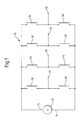
- a circuit comprising a three phase electrical converter 10 with a neutral is shown in Figure 1.
- the circuit 10 comprises a voltage source 12 which has output terminals 14 and 16, a first pair of switches 18 and 20 which releasably electrically connect the output terminals 14 and 16 to a first phase output 22, a second pair of switches 24 and 26 which releasably electrically connect the output terminals 14 and 16 to a second phase output 28, a third pair of switches 30 and 32 which releasably electrically connect the output terminals 14 and 16 to the third phase output 34 and a fourth pair of switches 36 and 38 which releasably electrically connect the output terminals 14 and 16 to a neutral output 40.
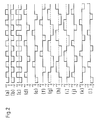
- the potential of the output terminals 14 and 16 of the voltage source 12 change between +V and O, and between O and -V respectively, and therefor the potential of output terminal 14 is always V volts above the potential of output terminal 16, as can be seen in graphs 2(a) and 2(b).
- the output terminals 14 and 16 of the voltage source 12 are electrically connected sequentially to the first phase output 22, the second phase output 28 and the third phase output 34, so that only one of the three phase outputs is electrically connected to the voltage source 12 at any time.
- the switches 18,20,24,26,30 and 32 perform the function of sequentially electrically connecting the three phase outputs to the voltage source 12.
- the voltage waveforms at the first phase output 22, the second phase output 28 and the third phase output 32 can be seen in graphs 2(d), 2(e) and 2(f) respectively.
- the switch 32 opens to disconnect the third phase output 34 from output terminal 16, as the switch 24 closes to connect the second phase output 28 to output terminal 14 which is at +V volts.
- Switch 24 opens, as the switch 20 closes to connect the first phase output 22 to output terminal 16 which is at -V volts.
- switch 30 closes to connect the third phase output 34 with the output terminal 14 which is at +V volts.
- the three phases of output are electrically connected sequentially to the output terminals of the voltage source by respective pairs of switches at a predetermined frequency to give the desired converter output frequency, the three phases of output are electrically connected to the output terminals with phase differences of 120° therebetween.
- Line voltages are obtained from the differences between the phase voltages as can be seen in graphs 2(g), 2(h) and 2(i). These are obtained respectively from the difference between the first phase output and the second phase output, the difference between the second phase output and the third phase output and the difference between the third phase output and the first phase output.
- the output terminals 14 and 16 of the voltage source 12 are also electrically connected sequentially to the neutral output 40.
- the switches 36 and 38 alternately connect the neutral output 40 to the output terminals 14 and 16 of the voltage source 12, such that the neutral output 40 is always connected to the output terminal which is at zero potential.
- the switches 36 and 38 in this example are opened and closed at three times the desired converter output frequency. It may be possible to open and close switches 36 and 38 at the desired converter output frequency, or at some other suitable multiple of the desired converter output frequency.
- Switching of the neutral output in this way alternately references the output terminals of the voltage source to earth, neutral, potential in turn.
- the lower potential of the output terminals is referenced to zero to obtain a positive output voltage in one circumstance, whilst in the other case the upper potential of the output terminals is references to zero to obtain a negative output voltage.
- a waveform illustrated in Figure 2(c) is produced across the input terminals of the three phase converter, and is in effect a bipolar square wave amplitude of ⁇ V volts.
- the line voltage waveforms shown in graphs 2(g), 2(h) and 2(i) contain less harmonic frequency components than the phase voltage waveforms shown in graphs 2(d), 2(e) and 2(f), owing to cancellation of harmonics between any two phase voltages. This results in filtering of the output voltages, to produce a purely sinusoidal waveform, being more readily achieved for the line voltage waveform than for the phase voltage waveform.
- the voltage source is a DC link capacitor
- the switches are power semiconductors of an appropriate type and power rating for the given application.
- the power semiconductors are transistors, as thyristors are not suitable because of the need for a short time between the switching actions.
- a more practical arrangement uses pulse width modulation techniques, this allows increased switching frequency to be used in order to improve the output waveforms and also allow variation in the output voltage by scaling the width of the pulses used.
- This arrangement is the same as the arrangement shown in Figure 1, and functions on the same principles as shown in Figure 2, but the neutral point is switched at a higher frequency to that discussed with reference to Figure 2.
- Figure 3 illustrates the arrangement for pulse width modulation techniques, in which the maximum output voltage is required from the converter, however reduced output voltages can be obtained by scaling down the width of the pulses. For full output voltage it is necessary to connect the voltage source to one of the three phase outputs throughout the complete output cycle, as opposed to the case where reduced output voltage is required when the voltage source is not connected at all times throughout the complete output cycle.
- Graphs 3(a), 3(b) and 3(c) illustrates the voltage waveforms at the first phase output 22, the second phase output 28 and the third phase output 34 respectively.
- Graphs 3(d) and 3(e) illustrate the operation of switches 36 and 38 respectively.
- Graphs 3(f), 3(g) and 3(h) illustrate the line voltages obtained from the differences between the phase voltages. These are obtained respectively by the difference between the first phase output and the second phase output, the difference between the second phase output and the third phase output, and the difference between the third phase output and the first phase output.
- the ratio of ⁇ 3 to 1 between the line voltages and phase voltages is maintained in this example, provided that the pulses 44 forming the phase voltages waveforms are constrained to lie in the region ⁇ 60° around the peak 42 of the sinusoid representing each phase output voltage i.e. shown in Figure 3(a). This effectively avoids negative pulses occurring in the positive half cycle of the line voltage waveforms, and vice-versa, which would distort the line voltage waveforms.
- This constraint results in a factor of three between the neutral switching frequency and the desired converter output frequency, but in this case it is a group of pulses which appear, rather than a single pulse associated with each of the three output phases in the first arrangement. It may be possible to use other suitable neutral switching frequencies, equal to or multiples of the desired converter output frequency.
- the switches require some form of timing mechanism which operates them, and keeps them in synchronisation, many such mechanisms are known and will not be discussed herein.
- the arrangement discussed is suitable for three phase DC to AC electrical converters, when it is necessary to provide power to a single phase load, or for three phase AC to AC electrical converters, when it is necessary to provide power to a single phase load.
- the present invention thus allows a three phase electrical converter to supply a single phase load by providing a commutated neutral point.
- the commutated neutral point being provided by the use of a pair of switches which alternately connect the neutral point with the output terminals of a voltage source.
Landscapes
- Engineering & Computer Science (AREA)
- Power Engineering (AREA)
- Ac-Ac Conversion (AREA)
- Inverter Devices (AREA)
Applications Claiming Priority (2)
| Application Number | Priority Date | Filing Date | Title |
|---|---|---|---|
| GB888805295A GB8805295D0 (en) | 1988-03-05 | 1988-03-05 | Three phase electrical converter with neutral |
| GB8805295 | 1988-03-05 |
Publications (2)
| Publication Number | Publication Date |
|---|---|
| EP0331849A2 true EP0331849A2 (de) | 1989-09-13 |
| EP0331849A3 EP0331849A3 (de) | 1990-01-17 |
Family
ID=10632919
Family Applications (1)
| Application Number | Title | Priority Date | Filing Date |
|---|---|---|---|
| EP88311877A Withdrawn EP0331849A3 (de) | 1988-03-05 | 1988-12-15 | Elektrischer Dreiphasenkonverter mit einem Neutralpunkt |
Country Status (4)
| Country | Link |
|---|---|
| EP (1) | EP0331849A3 (de) |
| JP (1) | JPH01268460A (de) |
| CN (1) | CN1035744A (de) |
| GB (1) | GB8805295D0 (de) |
Cited By (1)
| Publication number | Priority date | Publication date | Assignee | Title |
|---|---|---|---|---|
| WO2001056133A1 (en) * | 2000-01-28 | 2001-08-02 | Newage International Limited | Ac power generating system |
Family Cites Families (3)
| Publication number | Priority date | Publication date | Assignee | Title |
|---|---|---|---|---|
| US3775663A (en) * | 1972-08-24 | 1973-11-27 | Gen Electric | Inverter with electronically controlled neutral terminal |
| US4507724A (en) * | 1983-10-17 | 1985-03-26 | Sundstrand Corporation | Pulse width modulated inverter for unbalanced and variable power factor loads |
| US4728806A (en) * | 1986-12-05 | 1988-03-01 | Westinghouse Electric Corp. | DC link variable speed constant frequency power source paralleling controls |
-
1988
- 1988-03-05 GB GB888805295A patent/GB8805295D0/en active Pending
- 1988-12-15 EP EP88311877A patent/EP0331849A3/de not_active Withdrawn
-
1989
- 1989-03-04 CN CN 89101234 patent/CN1035744A/zh active Pending
- 1989-03-06 JP JP1053597A patent/JPH01268460A/ja active Pending
Cited By (2)
| Publication number | Priority date | Publication date | Assignee | Title |
|---|---|---|---|---|
| WO2001056133A1 (en) * | 2000-01-28 | 2001-08-02 | Newage International Limited | Ac power generating system |
| US6801019B2 (en) | 2000-01-28 | 2004-10-05 | Newage International Limited | AC power generating system |
Also Published As
| Publication number | Publication date |
|---|---|
| GB8805295D0 (en) | 1988-04-07 |
| CN1035744A (zh) | 1989-09-20 |
| JPH01268460A (ja) | 1989-10-26 |
| EP0331849A3 (de) | 1990-01-17 |
Similar Documents
| Publication | Publication Date | Title |
|---|---|---|
| US5734565A (en) | Reducing switching losses in series connected bridge inverters and amplifiers | |
| US6154378A (en) | Polyphase inverter with neutral-leg inductor | |
| Rodriguez | A new control technique for AC-AC converters | |
| US4564895A (en) | Neutrally clamped PWM half-bridge inverter | |
| US3775663A (en) | Inverter with electronically controlled neutral terminal | |
| KR920017340A (ko) | 교류 모터 구동 시스템 | |
| JPH03502399A (ja) | 平衡変圧器を有した三相インバータの電源 | |
| Almakhles et al. | Switched capacitor-based 13L inverter topology for high-frequency AC power distribution system | |
| US6147887A (en) | Inverter utilizing a bootstrap method | |
| Kishore et al. | A novel three-phase multilevel inverter cascaded by three-phase two-level inverter and two single-phase boosted H-bridge inverters | |
| Thiyagarajan | Simulation analysis of 51-level inverter topology with reduced switch count | |
| EP0065396A2 (de) | Gleichstrom-Wechselstrom-Umformer | |
| Veenstra et al. | PWM-control of multi-level voltage-source inverters | |
| US4137570A (en) | Waveform synthesizer | |
| JP3784541B2 (ja) | 交流グリッドシステムへの無効電力の供給方法およびこの方法に用いるインバータ | |
| RU2204880C2 (ru) | Многоуровневый автономный инвертор фазных напряжений | |
| JPS6036711B2 (ja) | インバ−タ装置 | |
| Kurwale et al. | Performance analysis of modular multilevel converter (MMC) with continuous and discontinuous pulse width modulation (PWM) | |
| JPH01268460A (ja) | 中立点付きの3相コンバータ | |
| Zygmanowski et al. | DC-link voltage balancing method for a hybrid asymmetric multilevel converter | |
| Sae-Sue et al. | Comparative performance evaluation of fixed and adaptive hysteresis band delta modulation techniques for UPS | |
| US3510751A (en) | Naturally sampled quad pulse width modulated inverter | |
| Sarkar et al. | High resolution m-cell symmetric cascaded H-Bridge multilevel inverter with one transistor clamped H-Bridge per phase | |
| Dehmlow et al. | Comparison of resonant converter topologies | |
| Kishore et al. | A novel three-phase 13-level cascaded hybrid-module based multilevel inverter with level-shifted PWM |
Legal Events
| Date | Code | Title | Description |
|---|---|---|---|
| PUAI | Public reference made under article 153(3) epc to a published international application that has entered the european phase |
Free format text: ORIGINAL CODE: 0009012 |
|
| AK | Designated contracting states |
Kind code of ref document: A2 Designated state(s): CH DE FR GB LI SE |
|
| PUAL | Search report despatched |
Free format text: ORIGINAL CODE: 0009013 |
|
| AK | Designated contracting states |
Kind code of ref document: A3 Designated state(s): CH DE FR GB LI SE |
|
| RHK1 | Main classification (correction) |
Ipc: H02M 7/5387 |
|
| STAA | Information on the status of an ep patent application or granted ep patent |
Free format text: STATUS: THE APPLICATION IS DEEMED TO BE WITHDRAWN |
|
| 18D | Application deemed to be withdrawn |
Effective date: 19900718 |