EP0332375A1 - Dispositif isolateur - Google Patents
Dispositif isolateur Download PDFInfo
- Publication number
- EP0332375A1 EP0332375A1 EP89302220A EP89302220A EP0332375A1 EP 0332375 A1 EP0332375 A1 EP 0332375A1 EP 89302220 A EP89302220 A EP 89302220A EP 89302220 A EP89302220 A EP 89302220A EP 0332375 A1 EP0332375 A1 EP 0332375A1
- Authority
- EP
- European Patent Office
- Prior art keywords
- fins
- rings
- insulator
- assembly
- assembly according
- Prior art date
- Legal status (The legal status is an assumption and is not a legal conclusion. Google has not performed a legal analysis and makes no representation as to the accuracy of the status listed.)
- Ceased
Links
- 239000012212 insulator Substances 0.000 title claims abstract description 39
- 239000004020 conductor Substances 0.000 claims abstract description 11
- 239000000463 material Substances 0.000 claims description 11
- OKTJSMMVPCPJKN-UHFFFAOYSA-N Carbon Chemical compound [C] OKTJSMMVPCPJKN-UHFFFAOYSA-N 0.000 claims description 4
- 239000004593 Epoxy Substances 0.000 claims description 3
- 229910002804 graphite Inorganic materials 0.000 claims description 3
- 239000010439 graphite Substances 0.000 claims description 3
- 238000010849 ion bombardment Methods 0.000 claims description 3
- 230000015556 catabolic process Effects 0.000 description 8
- 150000002500 ions Chemical class 0.000 description 7
- 239000007789 gas Substances 0.000 description 4
- AZDRQVAHHNSJOQ-UHFFFAOYSA-N alumane Chemical group [AlH3] AZDRQVAHHNSJOQ-UHFFFAOYSA-N 0.000 description 3
- 239000011248 coating agent Substances 0.000 description 3
- 238000000576 coating method Methods 0.000 description 3
- 239000011521 glass Substances 0.000 description 3
- 239000002245 particle Substances 0.000 description 3
- XAGFODPZIPBFFR-UHFFFAOYSA-N aluminium Chemical compound [Al] XAGFODPZIPBFFR-UHFFFAOYSA-N 0.000 description 2
- 229910052782 aluminium Inorganic materials 0.000 description 2
- 230000000712 assembly Effects 0.000 description 2
- 238000000429 assembly Methods 0.000 description 2
- 230000015572 biosynthetic process Effects 0.000 description 2
- 230000000903 blocking effect Effects 0.000 description 2
- 230000005684 electric field Effects 0.000 description 2
- 238000004519 manufacturing process Methods 0.000 description 2
- 230000013011 mating Effects 0.000 description 2
- 229920004142 LEXAN™ Polymers 0.000 description 1
- 239000004418 Lexan Substances 0.000 description 1
- 240000005561 Musa balbisiana Species 0.000 description 1
- 235000018290 Musa x paradisiaca Nutrition 0.000 description 1
- 239000003990 capacitor Substances 0.000 description 1
- 229910052799 carbon Inorganic materials 0.000 description 1
- 238000010276 construction Methods 0.000 description 1
- 238000001816 cooling Methods 0.000 description 1
- 230000000694 effects Effects 0.000 description 1
- 230000017525 heat dissipation Effects 0.000 description 1
- 230000037431 insertion Effects 0.000 description 1
- 238000003780 insertion Methods 0.000 description 1
- 239000004431 polycarbonate resin Substances 0.000 description 1
- 229920005668 polycarbonate resin Polymers 0.000 description 1
- 238000007493 shaping process Methods 0.000 description 1
- 229920001169 thermoplastic Polymers 0.000 description 1
- 239000004416 thermosoftening plastic Substances 0.000 description 1
Images

Classifications
-
- H—ELECTRICITY
- H01—ELECTRIC ELEMENTS
- H01B—CABLES; CONDUCTORS; INSULATORS; SELECTION OF MATERIALS FOR THEIR CONDUCTIVE, INSULATING OR DIELECTRIC PROPERTIES
- H01B17/00—Insulators or insulating bodies characterised by their form
- H01B17/42—Means for obtaining improved distribution of voltage; Protection against arc discharges
Definitions
- This invention relates to an insulator assembly and more particularly to such an assembly for use in a plasma environment, such as would be experienced by a satellite in low earth orbit.
- a satellite in low earth orbit encounters a plasma environment having low background pressures and high electron and ion densities.
- the background pressures can be about 0.0001333 N/m2 (10 ⁇ 7 torr) while the electron and ion densities may be about 105/cm3.
- Standard insulator assemblies have proved unsuitable for use in such an environment when the voltage is above a few hundred volts. In such a low background pressure, the insulator outgasses and desorbs adsorbed or absorbed gasses. This results in higher local pressure near the insulator. These gasses ionize and ions impinge on the insulator surface causing secondary electron emission. Above a few hundred volts, these conditions result in flashovers on the insulator surface.
- a very high voltage (up to one million volts) insulator bushing assembly has been proposed (see US-A-3126439) for bringing a conductor into a vacuum vessel.
- This assembly includes an inner tube of a resistive material receiving the conductor.
- a stack formed by alternating annular glass members and aluminum rings surrounds the tube with the rings engaging the tube.
- a field-shaping ring is held by each aluminum ring to partially cover adjacent glass members.
- the tube is contracted by cooling or vacuum and, after insertion into the rings, is allowed to expand.
- an insulator assembly for use in a plasma environment comprising an elongate cylindrical member of insulative material, characterised by a plurality of resistive rings positioned about said member, and a plurality of annular metallic fins disposed about said member, one of said fins being disposed between each pair of adjacent rings, said fins extending outwardly beyond said rings whereby said rings provide voltage grading along said member and said fins serve to reduce the distance between conductive components between the ends of said member to limit avalanche growth of electrons.
- the assembly of the invention functions to provide a voltage grading along its length, which voltage grading results in conduction current to provide for removal of accumulated charges on the surface of the assembly.
- the assembly also operates to limit avalanche growth of electrons by limiting the distance between conductive members along the length of the insulator. Furthermore, the assembly limits the number of charged particles impinging on the surfaces of the insulator which otherwise would result in charging currents.
- the assembly of the invention is reliable in use, has long service life and is relatively easy and economical to manufacture.
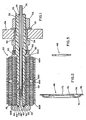
- a high voltage bushing assembly according to the invention is generally indicated in FIG. 1 by reference numeral 20.
- the assembly 20 is particularly intended for use in a plasma environment characterised by low background pressure and high electron and ion densities.
- the assembly 20, which has a total length less than 230 mm, can withstand an applied voltage of 12 kV without flashover assuming electron densities of 105/cm3, the voltage being between a high voltage terminal 22 at one end of the assembly and a wall 24 of a container, such as a pressure vessel, a transformer or a capacitor, on which the assembly is mounted.
- the assembly includes an elongate tubular insulator 26 having a central bore 28 which receives a conductor 30.
- the insulator 26 includes a first portion 32 extending through an opening 34 in the wall 24, and a second portion 35 extending away from the wall 24.
- the conductor 30 shown is a coaxial cable with its shield (not shown) connected to the wall 24 and its core 36 terminated in a banana plug 38 the spring tip of which is received in a socket defined by the stem 40 of the terminal 22.
- the stem 40 has an external screw thread mating with an internal thread in the bore 28 to hold the terminal 22.
- the underside 42 of the crown 44 of the terminal has a first annular groove 46 receiving the outer free end of the insulator 26, and a second annular grove 48, opening onto groove 46 receiving an O-ring 50 to establish a gas tight seal between the crown and the insulator 26.
- the insulator 26 is preferably formed of Lexan (a registered trademark of the General Electric Co. for thermoplastic polycarbonate resin).
- the first portion 32 of the insulator 26 extends through the bore of a mounting means in the form of a gas tight male connector assembly 52 having a base 54 with an external screw thread mating with an internal thread defining the wall opening 34.
- This connector assembly is commercially available, an example being the ULTRA-TORR male connector manufactured by the Cajon Company, Solin, Ohio. Accordingly this assembly will not be further described here.
- the insulator first portion 32 has an external screw thread for engagement by a nut 56 on the inside of the wall 24 and spaced therefrom by a washer 58.
- a washer 62 Seated by a shoulder 60 on the insulator 26 is a washer 62 which serves as an annular abutment receiving the insulator 26.
- a second washer 64 engaged by the underside 42 of the terminal crown 44 serves as a second abutment receiving the insulator 26.
- Compressively held between these abutments is a stack formed by a plurality of resistive rings 66 and a plurality of annular metallic fins 68, with one of the fins 68 being positioned between each part of adjacent rings 66.
- One of the fins 68 is best shown in FIG. 2, while a resistive ring 66 is best shown in FIG. 3.
- each rings there are preferably about thirty six rings including an innermost ring 66A in full surface engagement with the washer 62 and another outermost ring 66B in full surface engagement with the washer 64.
- each fin 68 is preferably formed of aluminum and includes a central section 70 defining an opening 72 receiving the second portion 35 of the insulator 26.
- the fin 68 further includes a skirt section 74 disposed outwardly of the central section and extending, as shown in FIG. 1, in the axial direction of the assembly 20 for shading one of the rings 66 from ion bombardment. More specifically the skirt section 74 is arcuate and folds back on itself, defining a cavity 76.
- the skirt section 74 of one fin extends into the cavity defined by the next adjacent fin 74 so that there is no linear path between these fins to the resistive ring 66 between the fins 74, thereby fully blocking linear motion ion impingement.
- the skirt section of the fin 68A extends toward the washer 62 to shade ring 66A, while the skirt section of the fin 68B extends toward the washer 64 to shade ring 66B.
- Fins 68A and 68C along with the fins disposed therebetween form an inner group of fins
- fins 68B and 68D along with the fins disposed therebetween form an outer group of fins.
- the pairs of adjacent fins, except for the pair formed by 68C and 68D, are substantially equally spaced, with the facing central sections 70 being in substantially full surface contact with the resistive ring 66 disposed therebetween.
- the fins are identical and have substantially uniform thickness.
- Each fin also includes an outer brim 78, extending generally normal to the axis of the assembly for further blocking ion impingement.
- the resistive rings 66 are identical and are formed of a material which is a bulk resistor, a preferred material being epoxy graphite. Upon tightening of the nut 56, the insulator 26 is drawn inwardly, causing the crown 44 to compress the stack of rings 66 and fins 68 between the washers 62 and 64. This establishes good electrical contact between adjacent rings and fins.
- FIG. 4 An equivalent circuit of the assembly 20 is shown in FIG. 4 in which the anode and cathode of the battery B are formed by the wall 24 and high voltage terminal 22, respectively.
- the resistor R is the equivalent of the stack of rings 66 while the current source 80, shunting resistor R, represents the current resulting from the plasma.
- FIG. 5 shows an exemplary Pashen curve, with the vertical axis representing the magnitude of breakdown voltage required for flashover and the horizontal axis being a measure of the product of distance between adjacent condutive members along the assembly outer surface multiplied by pressure. Note that the lowest breakdown voltage occurs at about 13.3N/m2 (.1 torr) centimeter.
- each ring 66 is about 500 k while the thickness of each ring 66 (also the spacing between adjacent fins) is 2.3 mm. If within the limits of the mechanical strength of the resistive material, the thickness can be further deceased, an even higher applied voltage can be withstood by the assembly.
- the resistivity of the rings 66 causes the conduction current through the assembly (less than 1 milliamp) to be greater than the plasma current. Secondary electrons from the fins 68 can replace electrons removed from the resistive rings 66 due to ion bombardment, thereby controlling charging of the rings 66.
- the rings 66 have sufficient thickness that the voltage drop across any one individual ring is below a voltage roughly corresponding to the Pashen minimum voltage for breakdown. Because there is already a plasma present in the space between the aluminum fins 68, the term "breakdown" has little meaning.
- resistive ring 66E is formed by an insulator 82 having an outer conductor coating 84.
- the insulator could be glass or procelain while the coating could be epoxy loaded with graphite. Accordingly with the stack formed by resistive rings 66E, a conduction current flows along the outer surface of the rings to achieve the same results discussed above.
- the use of the resistive ring 77 formed of a material which is a bulk resistor is generally preferred due to the much greater cross section through which the current flows to achieve significantly greater heat dissipation.
- the bushing of FIG. 1 can be made into an insulator by simply not using the conductor 30 or by replacing the insulator 26 with a cylindrical member of insulative material. The device can then be used to hold a component, such as a high voltage conductor, spaced from a support such as the wall 24.
Landscapes
- Engineering & Computer Science (AREA)
- Power Engineering (AREA)
- Insulators (AREA)
Applications Claiming Priority (2)
| Application Number | Priority Date | Filing Date | Title |
|---|---|---|---|
| US165618 | 1988-03-08 | ||
| US07/165,618 US4835341A (en) | 1988-03-08 | 1988-03-08 | Electrical insulator for use in plasma environment |
Publications (1)
| Publication Number | Publication Date |
|---|---|
| EP0332375A1 true EP0332375A1 (fr) | 1989-09-13 |
Family
ID=22599678
Family Applications (1)
| Application Number | Title | Priority Date | Filing Date |
|---|---|---|---|
| EP89302220A Ceased EP0332375A1 (fr) | 1988-03-08 | 1989-03-06 | Dispositif isolateur |
Country Status (4)
| Country | Link |
|---|---|
| US (1) | US4835341A (fr) |
| EP (1) | EP0332375A1 (fr) |
| JP (1) | JPH0272516A (fr) |
| CA (1) | CA1314597C (fr) |
Families Citing this family (5)
| Publication number | Priority date | Publication date | Assignee | Title |
|---|---|---|---|---|
| US6368451B1 (en) * | 2000-02-09 | 2002-04-09 | Delphi Technologies, Inc. | High voltage feedthrough for non-thermal plasma reactor |
| US6397662B1 (en) * | 2000-02-16 | 2002-06-04 | Can-Best Building Sciences Corporation | Gas concentration meter and insulating glass assembly and method thereof |
| US7059249B2 (en) * | 2001-01-23 | 2006-06-13 | United Defense Lp | Transverse plasma injector ignitor |
| DE102010005086B4 (de) * | 2010-01-15 | 2018-05-24 | Siemens Aktiengesellschaft | Hochspannungsdurchführung |
| US20120032772A1 (en) * | 2010-08-04 | 2012-02-09 | Cooper Technologies Company | Joining a current limiting device and a fuse |
Citations (3)
| Publication number | Priority date | Publication date | Assignee | Title |
|---|---|---|---|---|
| US3126439A (en) * | 1964-03-24 | High-voltage electrical insulating bushing | ||
| FR1400522A (fr) * | 1964-04-15 | 1965-05-28 | Coq France | Support électro-isolant haute tension |
| US4107455A (en) * | 1977-06-02 | 1978-08-15 | Richards Clyde N | Linear insulator with alternating nonconductive sheds and conductive shields |
Family Cites Families (10)
| Publication number | Priority date | Publication date | Assignee | Title |
|---|---|---|---|---|
| US1199467A (en) * | 1914-06-09 | 1916-09-26 | Westinghouse Electric & Mfg Co | Iron-porcelain insulating-bushing. |
| US2209003A (en) * | 1939-01-31 | 1940-07-23 | Ohio Brass Co | Bushing insulator |
| US3627906A (en) * | 1970-09-24 | 1971-12-14 | Westinghouse Electric Corp | Electrical condenser bushing assembly |
| GB1451071A (en) * | 1973-02-17 | 1976-09-29 | Trans Dev Ltd | High voltage electric insulator termination constructions |
| US3967051A (en) * | 1975-05-22 | 1976-06-29 | Westinghouse Electric Corporation | Cast resin capacitor bushing having spacer members between the capacitor sections and method of making same |
| SU803017A1 (ru) * | 1978-07-31 | 1981-02-07 | Научно-Исследовательский Институтвысоких Напряжений При Томскомордена Октябрьской Революции Иордена Трудового Красного Знамениполитехническом Институте Им.C.M.Кирова | Секционированный электрическийизОл ТОР |
| US4255615A (en) * | 1979-09-24 | 1981-03-10 | The United States Of America As Represented By The Secretary Of The Navy | Dielectric corona rings |
| EP0068067B1 (fr) * | 1981-06-26 | 1985-11-06 | Manoranjan Prasad Dr.-Ing. Verma | Résistance à haute tension pour isolateurs de lignes aériennes |
| CH659550A5 (de) * | 1983-03-21 | 1987-01-30 | Bbc Brown Boveri & Cie | Spannungsbegrenzende durchfuehrung. |
| FR2545259B1 (fr) * | 1983-04-29 | 1985-12-27 | Ceraver | Isolateur electrique presentant une insensibilite amelioree a la pollution |
-
1988
- 1988-03-08 US US07/165,618 patent/US4835341A/en not_active Expired - Fee Related
-
1989
- 1989-03-06 EP EP89302220A patent/EP0332375A1/fr not_active Ceased
- 1989-03-08 JP JP1055974A patent/JPH0272516A/ja active Pending
- 1989-03-08 CA CA000593106A patent/CA1314597C/fr not_active Expired - Fee Related
Patent Citations (3)
| Publication number | Priority date | Publication date | Assignee | Title |
|---|---|---|---|---|
| US3126439A (en) * | 1964-03-24 | High-voltage electrical insulating bushing | ||
| FR1400522A (fr) * | 1964-04-15 | 1965-05-28 | Coq France | Support électro-isolant haute tension |
| US4107455A (en) * | 1977-06-02 | 1978-08-15 | Richards Clyde N | Linear insulator with alternating nonconductive sheds and conductive shields |
Non-Patent Citations (1)
| Title |
|---|
| J.M. MEEK AND J.D. CRAGGS: "ELECTRICAL BREAKDOWN OF GASES" 1953, OXFORD PRESS, OXFOERD * |
Also Published As
| Publication number | Publication date |
|---|---|
| JPH0272516A (ja) | 1990-03-12 |
| CA1314597C (fr) | 1993-03-16 |
| US4835341A (en) | 1989-05-30 |
Similar Documents
| Publication | Publication Date | Title |
|---|---|---|
| US4241374A (en) | Surge voltage arrester with ventsafe feature | |
| US3663928A (en) | Electrical bushing assembly | |
| US3702952A (en) | Gas tube surge protective device and method for making the device | |
| EP0309978B1 (fr) | Interrupteur à vide | |
| US5936822A (en) | Coaxial surge arrester | |
| US4835341A (en) | Electrical insulator for use in plasma environment | |
| US4053802A (en) | High-voltage vacuum tube, particularly an x-ray tube | |
| US4773871A (en) | High voltage bulkhead coupling | |
| Allen et al. | The role of negative ions in the propagation of discharges across insulating surfaces | |
| CA1287871C (fr) | Eclacteur a gaz | |
| US4603368A (en) | Voltage arrester with auxiliary air gap | |
| US3858077A (en) | Gas tube transient voltage protector for telecommunication systems | |
| Al-Bawy et al. | Insulator flashover in SF6 under impulse voltage conditions | |
| US4187526A (en) | Gas-Discharge surge arrester with concentric electrodes | |
| Malik et al. | The influence of voltage polarity and field non-unifornity on the breakdown behavior of rod-plane gaps filled with SF6 | |
| CA1289615C (fr) | Eclateur a courants intenses a controle ameliore du niveau de decharge pour ligne d'alimentation | |
| US2414308A (en) | Protective gap device | |
| US1790152A (en) | Electrical discharge apparatus | |
| JP4291013B2 (ja) | 真空バルブ | |
| US4471264A (en) | Cathode ray tube | |
| US2833953A (en) | High voltage electron tube | |
| CN1918760A (zh) | 火花间隙避雷器 | |
| US6280215B1 (en) | Electrode receptacle plug and method | |
| JPS63502232A (ja) | 内燃機関の点火プラグの特に予備火花ギヤップとして使用のための火花ギヤップ | |
| EP0044894A1 (fr) | Dérivateur de surtension avec disposition de sécurité de fonctionnement en cas de fuite de gaz |
Legal Events
| Date | Code | Title | Description |
|---|---|---|---|
| PUAI | Public reference made under article 153(3) epc to a published international application that has entered the european phase |
Free format text: ORIGINAL CODE: 0009012 |
|
| AK | Designated contracting states |
Kind code of ref document: A1 Designated state(s): AT BE CH DE FR GB IT LI LU NL SE |
|
| 17P | Request for examination filed |
Effective date: 19900312 |
|
| 17Q | First examination report despatched |
Effective date: 19920402 |
|
| STAA | Information on the status of an ep patent application or granted ep patent |
Free format text: STATUS: THE APPLICATION HAS BEEN REFUSED |
|
| 18R | Application refused |
Effective date: 19930506 |