EP0332486A1 - Matrix photoempfindlicher Elemente und Strahlungssensor mit einer solchen Matrix, insbesondere Doppel-Energie-Röntgensensor - Google Patents
Matrix photoempfindlicher Elemente und Strahlungssensor mit einer solchen Matrix, insbesondere Doppel-Energie-Röntgensensor Download PDFInfo
- Publication number
- EP0332486A1 EP0332486A1 EP89400446A EP89400446A EP0332486A1 EP 0332486 A1 EP0332486 A1 EP 0332486A1 EP 89400446 A EP89400446 A EP 89400446A EP 89400446 A EP89400446 A EP 89400446A EP 0332486 A1 EP0332486 A1 EP 0332486A1
- Authority
- EP
- European Patent Office
- Prior art keywords
- photosensitive
- matrix
- photosensitive elements
- point
- photodiodes
- Prior art date
- Legal status (The legal status is an assumption and is not a legal conclusion. Google has not performed a legal analysis and makes no representation as to the accuracy of the status listed.)
- Ceased
Links
- 239000011159 matrix material Substances 0.000 title claims abstract description 54
- 239000004020 conductor Substances 0.000 claims abstract description 65
- 239000003990 capacitor Substances 0.000 claims abstract description 25
- 238000005286 illumination Methods 0.000 claims abstract description 13
- 230000002441 reversible effect Effects 0.000 claims description 18
- 239000000758 substrate Substances 0.000 claims description 17
- 230000005855 radiation Effects 0.000 claims description 16
- 239000000126 substance Substances 0.000 claims description 9
- 230000004044 response Effects 0.000 claims description 3
- 229910021417 amorphous silicon Inorganic materials 0.000 description 11
- 230000010354 integration Effects 0.000 description 9
- 230000007423 decrease Effects 0.000 description 8
- 230000035945 sensitivity Effects 0.000 description 8
- 238000010586 diagram Methods 0.000 description 5
- 239000012535 impurity Substances 0.000 description 5
- 238000004519 manufacturing process Methods 0.000 description 5
- 239000000463 material Substances 0.000 description 5
- 230000010287 polarization Effects 0.000 description 5
- 238000010521 absorption reaction Methods 0.000 description 3
- 238000006243 chemical reaction Methods 0.000 description 3
- 238000000034 method Methods 0.000 description 3
- 238000001228 spectrum Methods 0.000 description 3
- XUIMIQQOPSSXEZ-UHFFFAOYSA-N Silicon Chemical compound [Si] XUIMIQQOPSSXEZ-UHFFFAOYSA-N 0.000 description 2
- 229910052771 Terbium Inorganic materials 0.000 description 2
- 238000003491 array Methods 0.000 description 2
- 230000008859 change Effects 0.000 description 2
- 239000011521 glass Substances 0.000 description 2
- AMGQUBHHOARCQH-UHFFFAOYSA-N indium;oxotin Chemical compound [In].[Sn]=O AMGQUBHHOARCQH-UHFFFAOYSA-N 0.000 description 2
- 238000002347 injection Methods 0.000 description 2
- 239000007924 injection Substances 0.000 description 2
- SIWVEOZUMHYXCS-UHFFFAOYSA-N oxo(oxoyttriooxy)yttrium Chemical compound O=[Y]O[Y]=O SIWVEOZUMHYXCS-UHFFFAOYSA-N 0.000 description 2
- 230000002829 reductive effect Effects 0.000 description 2
- 238000000926 separation method Methods 0.000 description 2
- 229910052710 silicon Inorganic materials 0.000 description 2
- 239000010703 silicon Substances 0.000 description 2
- 238000003860 storage Methods 0.000 description 2
- GZCRRIHWUXGPOV-UHFFFAOYSA-N terbium atom Chemical compound [Tb] GZCRRIHWUXGPOV-UHFFFAOYSA-N 0.000 description 2
- ZOXJGFHDIHLPTG-UHFFFAOYSA-N Boron Chemical compound [B] ZOXJGFHDIHLPTG-UHFFFAOYSA-N 0.000 description 1
- PTOAARAWEBMLNO-KVQBGUIXSA-N Cladribine Chemical compound C1=NC=2C(N)=NC(Cl)=NC=2N1[C@H]1C[C@H](O)[C@@H](CO)O1 PTOAARAWEBMLNO-KVQBGUIXSA-N 0.000 description 1
- OAICVXFJPJFONN-UHFFFAOYSA-N Phosphorus Chemical compound [P] OAICVXFJPJFONN-UHFFFAOYSA-N 0.000 description 1
- 229910052581 Si3N4 Inorganic materials 0.000 description 1
- MCVAAHQLXUXWLC-UHFFFAOYSA-N [O-2].[O-2].[S-2].[Gd+3].[Gd+3] Chemical compound [O-2].[O-2].[S-2].[Gd+3].[Gd+3] MCVAAHQLXUXWLC-UHFFFAOYSA-N 0.000 description 1
- 230000002238 attenuated effect Effects 0.000 description 1
- 230000004888 barrier function Effects 0.000 description 1
- 229910052796 boron Inorganic materials 0.000 description 1
- 238000002144 chemical decomposition reaction Methods 0.000 description 1
- 230000003247 decreasing effect Effects 0.000 description 1
- 238000000151 deposition Methods 0.000 description 1
- 238000009792 diffusion process Methods 0.000 description 1
- 238000009826 distribution Methods 0.000 description 1
- 230000009977 dual effect Effects 0.000 description 1
- 238000005530 etching Methods 0.000 description 1
- 230000005284 excitation Effects 0.000 description 1
- DQZARQCHJNPXQP-UHFFFAOYSA-N gadolinium;sulfur monoxide Chemical compound [Gd].S=O DQZARQCHJNPXQP-UHFFFAOYSA-N 0.000 description 1
- 238000003384 imaging method Methods 0.000 description 1
- 230000000670 limiting effect Effects 0.000 description 1
- 230000003287 optical effect Effects 0.000 description 1
- 229910052698 phosphorus Inorganic materials 0.000 description 1
- 239000011574 phosphorus Substances 0.000 description 1
- 239000000843 powder Substances 0.000 description 1
- 230000008569 process Effects 0.000 description 1
- 230000001737 promoting effect Effects 0.000 description 1
- 239000011347 resin Substances 0.000 description 1
- 229920005989 resin Polymers 0.000 description 1
- 239000004065 semiconductor Substances 0.000 description 1
- HQVNEWCFYHHQES-UHFFFAOYSA-N silicon nitride Chemical compound N12[Si]34N5[Si]62N3[Si]51N64 HQVNEWCFYHHQES-UHFFFAOYSA-N 0.000 description 1
- XUIMIQQOPSSXEZ-RNFDNDRNSA-N silicon-32 atom Chemical compound [32Si] XUIMIQQOPSSXEZ-RNFDNDRNSA-N 0.000 description 1
- 239000000243 solution Substances 0.000 description 1
- 230000006641 stabilisation Effects 0.000 description 1
- 238000011105 stabilization Methods 0.000 description 1
- 229920001187 thermosetting polymer Polymers 0.000 description 1
Images

Classifications
-
- H—ELECTRICITY
- H05—ELECTRIC TECHNIQUES NOT OTHERWISE PROVIDED FOR
- H05G—X-RAY TECHNIQUE
- H05G1/00—X-ray apparatus involving X-ray tubes; Circuits therefor
- H05G1/08—Electrical details
- H05G1/60—Circuit arrangements for obtaining a series of X-ray photographs or for X-ray cinematography
-
- H—ELECTRICITY
- H04—ELECTRIC COMMUNICATION TECHNIQUE
- H04N—PICTORIAL COMMUNICATION, e.g. TELEVISION
- H04N25/00—Circuitry of solid-state image sensors [SSIS]; Control thereof
- H04N25/70—SSIS architectures; Circuits associated therewith
- H04N25/76—Addressed sensors, e.g. MOS or CMOS sensors
-
- H—ELECTRICITY
- H04—ELECTRIC COMMUNICATION TECHNIQUE
- H04N—PICTORIAL COMMUNICATION, e.g. TELEVISION
- H04N5/00—Details of television systems
- H04N5/30—Transforming light or analogous information into electric information
- H04N5/32—Transforming X-rays
- H04N5/3205—Transforming X-rays using subtraction imaging techniques
Definitions
- the invention relates to the development of images by means of arrays of photosensitive elements, and more particularly relates to a matrix arrangement of photosensitive elements allowing the simultaneous acquisition of several images.
- the invention also relates to a radiation detector using such an arrangement of photosensitive elements, in particular an X-ray detector making it possible to simultaneously develop two images each corresponding to an energy spectrum different from X-radiation.
- Images of this type or dual-energy images, currently produced by radiologists, are obtained from two images of the same area of the patient formed successively, either by modifying from one image to another the X-ray conditions.
- energy spectrum of different X-rays either by using sensors sensitive to energy windows different from X-rays, this being obtained for example by changing the type of scintillator used to convert the X-rays into visible light which impresses a photographic film
- the scintillator is a substance which has the property of being excited by X-rays and emitting, in response to this excitation, radiation of visible or near-visible wavelength; the scintillator has a yield maximum conversion, or maximum sensitivity, in a certain energy range of X-rays, this energy range being determined by the nature of the substance which constitutes the scintillator).
- One of the aims of the invention is to allow the production of two simultaneous images called dual-energy images of the same examined area, each corresponding to an energy spectrum different from X-ray radiation, so as to allow perfect superimposability of the images. .
- This is obtained using a surface sensor of the type comprising a matrix of photosensitive elements, therefore requiring no mechanical movement during the taking of images and providing from a single x irradiation of an object or patient, the above two images.
- each photosensitive point is connected between a row conductor and a column conductor. In fact, to each row conductor is connected as many photosensitive dots as there are columns of these, and to each column conductor is connected as many photosensitive dots as there are rows of these.
- each photosensitive point is made up by a photodiode in series with a capacitance; the capacity serving, on the one hand, to store the charges generated by an illumination of the photodiode, and serving on the other hand to isolate the photodiode from the column conductor when the line corresponding to this photodiode is not selected, during reading the photosensitive dot.
- n ° 86 00716 published under n ° 2 593 343 describes a method of manufacturing a matrix of photosensitive dots as explained above as well as a method of reading and applying this matrix to the socket view of images, in particular radiological images.
- One of the advantages of this type of structure is that it makes it possible to produce matrices of large dimensions, because the thin layer deposits, of amorphous silicon for example, are now well controlled.
- Another object of the invention is therefore to allow the production of photosensitive detectors, of linear or matrix type, each photosensitive point of which is capable of storing two different pieces of information, thus making it possible in particular to obtain with a radiological image detector, two images each corresponding to a different energy from the X-ray and each having a resolution and a filling factor equivalent to the mono energy images.
- a matrix of photosensitive elements comprising a network of conductors in line and a network of conductors in column, a network of photosensitive points, is characterized in that each photosensitive point comprises, between a line conductor and a conductor column, two photosensitive elements mounted in series with a capacity, the two photosensitive elements being mounted head to tail.
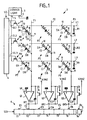
- Figure 1 shows a photosensitive matrix 1 according to the invention.
- the matrix 1 comprises a network of conductors in line L1, L2, L3 and a network of conductors in column F1, F2, F3; in the nonlimiting example described, these two types of conductors are each limited to 3, to simplify FIG. 1.
- the matrix 1 comprises a network of photosensitive points P1, P2, ..., P9 also organized in rows and columns , and which are arranged at the intersection of the line conductors L1 to L3 and the column conductors F1 to F3; each sensitive point P1 to P9 having one end 10 connected to a row conductor L1 to L3, and a second end 11 connected to a column conductor F1 to F3.
- the photosensitive points P1, P2, ..., P9 each consist of a first and a second photosensitive elements DA, DB arranged in series with a capacity CI, the two photosensitive elements DA, DB being arranged head to tail, that is to say that they have reversed directions of conduction.
- the photosensitive elements DA, DB are constituted by photodiodes, and the capacitor CI is arranged between the two photodiodes.
- each of the photosensitive points P1 to P9 can store two different pieces of information, so for example to produce two radiological images each corresponding to a different energy of the X-ray radiation.
- This can be obtained by converting the X-ray into visible light and by exposing each photodiode DA, DB to the light having the desired origin, which allows on the one hand, in a zone A located between a first armature 7 of the capacitance CI and the cathode of the first photodiode DA, and forming a first point at floating potential, to store a first item of information or quantity of charge QA linked to the illumination of the first photodiode DA; and on the other hand, in a second zone B, forming a second point with floating potential situated between the second armature 8 of the capacitance CI and the cathode of the second photodiode DB, to store a second information or quantity of charge QB linked to the illumination of the second photodiode DB.
- the information or charges QA or QB are generated and stored when the photodiode DA or DB is reverse biased, according to an operation similar to that which is explained for a cell with a photodiode and a capacity in the French patent applications n ° 86 000656 and 86 00716 already cited.
- the reading of the storage areas A, B is then carried out by a direct polarization reset of the photodiodes A, B.
- the line conductors L1 to L3 are connected to an output terminal 5 of the pulse generator 3 by means of MOS transistors M1, M2, M3 forming line switches controlled by the outputs OL1, OL2, OL3 of a shift register 4 called the line register.
- This register is controlled by a line shift control signal SCL. So when a line of photosensitive points P1 to P3 or P4 to P6 or P7 to P9 is selected, the corresponding line conductor L1 to L3 is connected to the pulse generator 3, so that the line signals are applied to all the points photosensitive connected to this line conductor.
- each line conductor L1, L2, L3 is connected to earth by a resistance R1, R2, R3; these resistors R1 to R3 having a high value compared to the resistance presented by the line switches M1 to M3 when the latter are closed (on state).
- each column conductor F1 to F3 is connected to the negative input "-" of an operational amplifier G1 to G3, mounted as an integrator using an integration capacitor CL1 to CL3.
- the integration capacitor CL1 to CL3 is mounted between the negative input "-" of the amplifier G1 to G3 and the output OF1, OF2, OF3 of the latter.
- the second input or positive "+” input of each amplifier G1 to G3 is connected to a column reference potential VF which, in the nonlimiting example described is ground.
- Each integrating amplifier G1 to G3 further includes a reset switch I1 to I3 mounted in parallel with the integration capacitor CL1 to CL3.
- the reset switch I1 to I3 of a given integrating amplifier G1 to G3 is kept closed so as to short-circuit the integration capacitor CL1 to CL3, except during the reading sequence of zones A, B of a photosensitive point which is connected to this amplifier.
- the switches I1 to I3 consist of MOS transistors controlled by reset signals V-RESET.
- the column conductors F1 to F3 are at zero volt or ground potential; the same is true for the line conductors L1 to L3, the voltage VL of the line signals being referenced with respect to ground, the second terminal 6 of the generator 3 is connected to ground.
- the outputs OF1, OF2, OF3 of the integrating amplifiers G1, G2, G3 are connected to reading and multiplexing means comprising an analog data acquisition device 6, constituted for example by a shift register with n acquisition stages T1, T2, ... Tn with parallel inputs E1, E2, ..., En and S serial output, of the CCD type for example.
- two acquisition stages adjacent are intended to be loaded successively by the same output OF1, OF2, OF3 of amplifier G1, G2, G3.
- the outputs OF1, OF2, OF3 are connected for example respectively to the second, fourth and sixth inputs E2, E4, E6 so as to first load the corresponding acquisition stages T2, T4, T6, then to secondly load the acquisition stages T1, T3, T5, after having effected an offset of the stages using a horizontal offset signal SCH applied to the control input 10 of the acquisition device 6.
- Reverse polarization of photodiodes DA, DB can be achieved either for all photosensitive points P1 to P9 simultaneously by switching all the line switches M1, M2, M3 on, or only for photosensitive points connected to the same line conductor: by example the first, second and third photosensitive points P1, P2, P3 if it is the first line switch M1 which is made conductive.
- the reading of a photosensitive point P1 to P9 can be carried out on the double condition that, the line conductor L1 to L3 to which it is connected is connected to the pulse generator 3 (corresponding line switch M1 to M3 being in the state passing), and that the integration capacitor CL1 to CL3, to which it is connected by a column conductor, is not short-circuited (corresponding reset switch being in the blocked or open state).
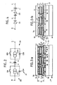
- FIG. 2 shows the equivalent diagram of a photosensitive point, the first photosensitive point P1 for example.
- each photosensitive diode DA, DB can be represented by three parallel elements, namely: - a capacity CDA, CDB, which is the capacity presented by the photodiode when it is reverse biased; - a current source IPA, IPB, which has the value of the photocurrent; - And a switch IDA, IDB which is on, that is to say closed when the photodiode DA, DB is forward biased and which is blocked, that is to say open when the photodiode is reverse biased.
- FIGS. 3a to 3f are diagrams which show the different signals applied or obtained during a complete operating cycle of a photosensitive point P1 to P9: - Figure 3a shows the line voltage VL, delivered by the pulse generator 3, and its evolution over a cycle; FIG. 3b illustrates the phase of illumination of the photosensitive elements DA, DB, that is to say in the case of radiological images, the phase of exposure to X-radiation of a patient; - Figure 3c illustrates the change of state of the reset switches I1 to I3 mounted in parallel on the integration capacitors CL1 to CL3 - Figure 3d shows a general reset step or RAN leveling of photosensitive elements; FIG. 3e and FIG. 3f respectively show the form of signals VA and VB established respectively at the zones or points A and B in relation to the application of the line voltage VL and the exposure to light of the photosensitive elements DA and DB.
- the line voltage VL is at zero and increases to reach a first positive value V1 of the order of 6 volts at an instant t1; the line voltage VL remains substantially stable until a second instant t2 from which it decreases to go through zero at an instant t3 (marking the end of a first positive pulse), and increase in negative until an instant t4 where it reaches a first negative value -V1, of about -9 volts; voltage line VL remains substantially stable at the value -V1 until an instant t5 where it decreases to return to zero at an instant t6 (marking the end of a first negative pulse). This constitutes a phase of reverse polarization of the photodiodes DA, DB.
- the voltages VA and VB are at zero before the instant t0 and follow the evolution of the line voltage VL but with different values. Indeed at time t1 the first photodiode DA is on while the second photodiode DB is blocked; also, between times t0 and t1 the voltage VB (shown in FIG. 3f) follows the voltage VL in the ratio CI / CI + CDB, (CDB being the equivalent capacity of the second photodiode DB) so that at instant t2 the voltage VB has a positive value of the order of 3V.
- the voltage VA at point A varies more slowly than the line voltage VL so that the first photodiode DA is blocked at from the third instant t2.
- the voltage VB at point B reaches 0 between time t3 and time t4
- the second photodiode DB becomes on and remains on until time t5 where the end of the negative level of line voltage VL is located; the voltage VA at point A then having a value of substantially -3 volts.
- the second photodiode DB is again reverse biased and then constitutes a CDB capacitance, and the voltages VA and VB respectively at points A and B vary in the same direction as the line voltage VL to each reach a positive voltage of the order of 3 volts, which represents the reverse bias voltage VPA, VPB of these photodiodes.
- the two photodiodes DA, DB are thus finally reverse biased, and it is noted that if the values V1, -V1 successively positive and negative of the line voltage VL have been well chosen, the two photodiodes DA, DB can be reverse biased to the same value, as in the example described.
- the two photodiodes DA, DB being reverse biased, they remain between time t6 and time t7 in a stabilization phase, then they are subjected to an exposure or lighting phase which results as it was previously mentioned, from the exposure of an object or a patient to X-rays.
- This lighting phase is symbolized in FIG. 4b, between an instant t7 and an instant t8.
- the photodiodes DA, DB generate photocharges and which are distributed over the capacities CDA, CI, CDB of the photosensitive point; consequently a load is injected on the column conductor, but this load is not taken into account by the amplifier-integrator G1 to G3, because the reset switch I1 to I3 is closed and short- thus circuits the integration capacitor CL1 to CL3.
- the voltages VA and VB at point A and B respectively can change depending on the intensity of this exposure, which exposure can of course be different for the first and for the second photodiode DA, DB.
- the first extreme case is represented by a curve 20 (in dashed lines), and corresponds to the case where the voltage VA at point A, which has the value of the bias voltage VPA, has been reduced to 0 volts as a result of the charges generated during the exposure period, while the point B has received no light so that the voltage VB has not been modified and has kept the value of the bias voltage VPB;
- a second curve 21 (in dashes) corresponds to the second extreme case, case opposite to that explained above, that is to say in the case where the voltage VB at point B has been reduced to 0 volts by the illumination , while point A has received no light:
- the third curve 22 in solid lines corresponds to the intermediate case where each of the photodiodes DA, DB has been lit, so that for example: the voltage VA at point A has been modified by the lighting and has been decreased to go from 3 volts to 2.5 volts for example; and that also the voltage VB at point B went from 3 volts to
- the reading phase begins with the application of a second positive pulse (shown in Figure 3a) on the line conductor, that is to say that the line voltage VL which is at 0 volts at time t10 passes , at time t11, at a positive voltage having a second value V2 greater than the first positive value V1, 9 volts for example: taking into account from the conditions described above, this value of 9 volts of the voltage VL is sufficient for the latter to catch up, before reaching its maximum, the value of the voltage VA at point A which of course also increases (as does the voltage VB in point B).
- a second positive pulse shown in Figure 3a
- the direct passage of the first photodiode DA modifies the distribution and the values of the charges accumulated on the various elements of the photosensitive point, and causes the injection of a third charge called reading charge Q1 on the column conductor and in the amplifier-integrator connected to it: this read charge Q1 is a linear combination of the first and second charge QA, QB or first and second information which themselves are respectively proportional to the illumination of the first and second element photosensitive DA, DB.
- the line voltage VL retains its second positive value V2 of 9 volts, which is also the case for the voltage VA at point A because the first photodiode DA is then conductive.
- the voltage VB at point B is also stable and, according to one of the previously mentioned cases, it can have a value of 7.5 volts in the first case represented by the first curve 20, or a value of 3 volts in the second case represented by the second curve 21, or a value of approximately 4.25 volts in the third intermediate case represented by the third curve 22.
- the switch I1 of R.A.Z. (fig. 3c) is then closed (state 1) so as to short-circuit and reset the integration capacitor CL1, then the switch I1 of R.A.Z. is again returned to the open state (state 0) in order to acquire a second read charge Q2.
- the line voltage VL decreases and goes through zero to reach a second negative level -V2 at an instant t13, this second negative voltage -V2 being of the order of -13.5 volts in the non-limiting example described.
- the first photodiode VA goes in reverse, then for a certain value of the line voltage VL, the second photodiode DB goes direct.
- the negative value of VL must then be such that the second diode DB always goes live: the most unfavorable case being that where the voltage VB at point B is maximum at time t12.
- the direct passage of the second photodiode DB modifies the values of the charges on the various elements of the photosensitive point and causes the injection of this second read charge Q2 into the amplifier-integrator G1.
- This second read charge Q2 is proportional to the second charge QB or second information QB generated at the second point B by the illumination of the second photosensitive element DB.
- the variation of the line voltage VL has generated, in the same direction, a variation of the voltages VA and VB: the voltage VA at point A has gone to a negative level which can have, according to the three cases previously mentioned, one of the three values represented by the first, second, third curves 20, 21, 22 and which correspond respectively in the nonlimiting example described at -3.75 volts, -6 volts and -4.37 volts ; at the same time the voltage VB at point B is at 0 volts, the second photodiode DB being direct, that is to say conductive.
- the line voltage VL returns to zero at time t15 and determines a variation in the same direction of the voltages VA and VB developed at points A and B. It it should be noted that at the same time, that is to say at time t14, the second read charge Q2 having been acquired, the switch I1 of RESET (fig.3c) is closed again. The points A and B then have a positive and stable voltage VA, VB, and the photodiodes DA and DB are both reverse biased.
- the R.A.N. is of the optical type: a sufficient quantity of light is sent to the photodiodes DA, DB to bring the voltages VA, VB from points A and B to O Volt, as shown in Figures 4e and 4f from time t16.
- QA and QB correspond respectively to the first and second information
- CI is the capacitance which, in a photosensitive point, is in series with the two photosensitive elements DA and DB
- CDA is the equivalent capacity of the first photosensitive element DA
- CDB is the equivalent capacity of the second photosensitive element DB
- This description of the operation of an isolated photosensitive element P1 can be applied to all of the photosensitive points P1 to P9, that is to say to all of the photosensitive matrix 1 represented in FIG. 1.
- the matrix comprises a number of row and column conductors L1 to L3 and C1 to C3 voluntarily limited for clarity of the description, and consequently this matrix comprises a small number of photosensitive points, but of course the invention can be applied to much larger photosensitive matrices, for example having several million photosensitive dots to form an image of 40 cm x 40 cm.
- the photosensitive matrix 1 according to the invention has the difference, in particular, that each photosensitive point from P1 to P9 can store two different pieces of information, so that the photosensitive matrix 1 of the invention makes it possible to acquire information relating to two different images simultaneously.
- the pulse generator 3 (represented in FIG. 1) sends on all the line conductors L1 to L3, simultaneously or with an offset, a positive pulse then a negative pulse (represented in FIG. 3a between the instant t0 and l 'instant t6; the duration for these two pulses can be between 1 and 5 ms). All DA and DB photodiodes are then reverse biased, and all R.A.Z. I1 to I3 are closed.
- the pulse generator 3 then delivers a second positive pulse, and a second negative pulse (shown in Figure 3a between time t10 and time t15).
- the switches of R.A.Z. I1 to I3 being open, we recover read charges Q1, Q2 which, in the form of voltage, are present at output OF1 to OF3 of amplifiers G1 to G3; these read charges Q1, Q2 making it possible to know the information QA, QB stored at points A and B. It should be noted that if the switches I1 to I3 are actuated according to the example shown in FIG. 3c, we first obtain Q1, then Q2; but we can also, if we leave the R.A.Z. I1 to I3 always open between time t9 and time t14, first obtain Q1, then Q1 + Q2.
- the information available at the output OF1 to OF3 of the amplifiers G1, G3 are loaded by the acquisition device 6 then sent to a computer (not shown, of conventional type) which calculates the values of the first and second loads or information QA and QB to from the read charges Q1 and Q2, the values of QA and QB being then stored.
- a computer not shown, of conventional type
- the other line conductors L2, L3 of the matrix 1 are maintained at zero, the duration of this phase being typically of the order of 1 ms.
- a general RAN leveling is then carried out, that is to say common to all the photosensitive points of the matrix 1, and the duration of which is for example of the order of 10 ms to 100 ms (this general refresher being symbolized in Figure 3d between time t16 and time t17).
- FIG. 4 shows a photosensitive point, the first photosensitive point P1 for example, in a form which differs from that shown in FIG. 1 in that the serial capacitance CI is no longer located between the two photodiodes DA, DB, but that the series assembly is constituted by a first and a second photodiodes DA, DB followed by the series capacity CI (or the reverse of course).
- the series assembly is constituted by a first and a second photodiodes DA, DB followed by the series capacity CI (or the reverse of course).
- the photodiodes DA, DB can be replaced by phototransistors, provided that the latter are well chosen, that is to say constituted for example by phototransistors of the NIPIN or PINIP type.
- FIGS. 5a and 5b are side sections in two orthogonal directions which show, by way of nonlimiting example and schematically, a preferred embodiment of a dual energy radiological image detector, comprising a photosensitive matrix as previously described.
- the image detector 25 comprises a support or substrate 26 made of glass for example.
- a scintillator layer 27 formed of a scintillator substance which is deposited on the substrate 26.
- the scintillating substance is chosen according to its maximum sensitivity in a certain energy range of the incident X-ray.
- gadolinium oxysulfide doped with terbium is known to have optimal sensitivity for X-rays whose energy is of the order of 50 KeV, and for emitting in response a green light of wavelength 0.54 micron.
- the scintillating layer 27 can be constituted by a gadolinium oxysulphide powder embedded in a thermosetting resin, so as to constitute a sheet; this sheet then being bonded to the substrate 26.
- the scintillator layer 27 has a thickness which is chosen to optimize the efficiency of photon production without losing too much on the resolution. This thickness can range from a few tens to a few hundred micrometers for radiological imaging applications.
- a thin conductive layer 28 of conductive material covers this scintillator layer 27, either directly or through, for example, an intermediate insulating layer (not shown) which allows in particular to planarize the upper surface of the scintillator layer 27 and to constitute a barrier to a diffusion of impurities.
- the thin conductive layer 28 can be made of indium tin oxide for example, and it is etched so as to constitute the column conductors such as the column conductors C1, C2, C3.
- the conductive layer 28 is in turn covered by a stack of several layers 30, 31, 32 which after etching constitute the second photodiodes DB previously described.
- the photodiodes DB are of the PIN type, that is to say that on the conductive layer 28 (intended to form the column conductors), there is firstly a layer 30 of amorphous silicon hydrogenated, for example by chemical decomposition in the gas phase (CVD); the hydrogenated amorphous silicon of this layer 30 being doped with a P-type impurity, for example boron.
- the layer 34 forming the dielectric of the capacitors CI is made of silicon nitride.
- the insulating layer 34 there is a second stack of three layers 40, 41, 42 which serve to constitute the first photodiodes DA; so that above the layer 34, there is successively a layer of hydrogenated amorphous silicon 40 doped with an N-type impurity, then a layer of intrinsic hydrogenated amorphous silicon 41, then a layer of hydrogenated amorphous silicon 42 doped with a type P impurity.
- the three layers 40, 41, 42 intended together to constitute the first photodiodes DA, and the insulating (dielectric) layer 34 are etched like the three layers 30, 31, 32, which form the second photodiode DB, c that is to say engraved according to a pattern of islands placed at each of the crossing points of the column conductors and the row conductors of the matrix.
- the capacitors CI being constituted by the insulating layer 34 located between two N-type regions which are formed by the layer 32 of the second photodiode DB, and by the layer 40 of the first photodiode DA.
- the production method can also consist in depositing, successively, all the layers 30, 31, 32, 34, 40, 41, 42 which constitute the two photodiodes DA, DB with, between these, the dielectric of the capacity CI, and then to engrave these layers in a single operation.
- This assembly is covered with a new insulating layer 50, which for example may be made of the same material as the insulating layer 34 which forms the dielectric of the capacitors CI.
- Openings are made in this last insulating layer 50 above the first photodiodes DA so as to make it possible to establish their contact with an upper conductive layer 51 which is etched to define the line conductors L1 to L3 of the matrix.
- the upper conductive layer 51 is transparent and it is made, for example, of indium tin oxide.
- a second scintillating layer 55 completes the structure, and covers the upper conductive layer 51 on which it is bonded or pressed with a transparent link to light (not shown).
- the scintillating substance which forms the second scintillating layer 55 is chosen as a function of the energy range of X-rays for which it has maximum sensitivity, this maximum sensitivity being of course presented for a range of energy of X-rays different from that of the first scintillator layer 27.
- this can be constituted by yttrium oxide so as to present an optimal sensitivity for X-rays of 20 KeV; the yttrium oxide of the second scintillating layer 55 can be doped, for example with terbium.
- the photosensitive points of the matrix are produced by a stack of layers in the direction of a thickness E of the matrix 1, namely three layers 30, 31, 32 for the second photodiodes DA, then a insulating layer 34 to form the capacitances CI, then three layers 40, 41, 42 to constitute the first photodiodes DA, all of these layers being arranged between conductive layers 28, 51 respectively forming the conductors of column and line conductors.
- One of the advantages of such a structure is to minimize the lateral space requirement of each photosensitive point for each of which two photodiodes DA, DB are thus superimposed.
- This structure is all the more advantageous since each point must be sensitive to (light) radiation of different origin, which is obtained by placing the matrix structure which has just been described sandwiched between the first and the second. scintillating layers 28.55.
- first scintillating layer SA taking account of the direction of propagation of the X-ray radiation.
- the X-ray radiation crosses first the first scintillating layer SA and the first photodiodes DA, then crosses then crosses the second photodiodes DB, and the other layer scintillator 27 or second scintillator layer SB situated between the substrate 26 and the second photodiodes DB.
- the x-ray is only absorbed significantly by the scintillators SA, SB, given the very thin thickness of the semiconductor layers, the thickest of which, the layers 31, 41, have a thickness of the order of 1 micrometer.
- the first SA scintillator mainly absorbs X-rays having a first energy range (around 20 KeV for example), and it converts the X-rays which it absorbs into radiation detectable by amorphous silicon.
- the second scintillator B mainly absorbs X-rays whose energy corresponds to its maximum sensitivity which is located at different energies (50 KeV for example) than in the case of the first SA scintillator, the absorbed X-rays being converted into detectable radiation by amorphous silicon.
- the first DA photodiodes located near the first scintillator SA preferentially collect the light emitted by the first scintillator SA
- the second photodiodes DB which are located near the second scintillator SB preferentially capture the light emitted by this second scintillator SB.
- amorphous silicon for example radiation and in particular the light emitted by the scintillating layers SA, SB, is absorbed or attenuated in the photosensitive material in such a way that the energy given up to this material decreases exponentially with the length of material crossed.
- the first and second diodes DA, DB and have respectively thicknesses E1, E2 comparable the light emitted by the first scintillating layer SA is absorbed and therefore detected essentially by the first photodiodes DA, and that the light emitted by the second scintillating layer SB is absorbed and detected essentially by the second photodiodes DB.
- the thicknesses E1, E2 of the photodiodes DA, DB are sufficient to completely absorb the radiation or light emitted by the scintillating layer which is closest, a total separation is obtained between the two pieces of information provided by the two scintillating layers SA and SB, and detected respectively by the first and second photodiodes DA and DB. It can be indicated by way of nonlimiting example, that satisfactory results have been obtained for thicknesses E1, E2 of photodiodes DA, DB of the order of 1 micron (we recall that the thickness E1, E2 is given essentially by the thickness of the intrinsic zone).
- Such an arrangement is particularly advantageous in that it allows the above-described layers to be superimposed by layers transparent to light, so that the previously mentioned RAN leveling can easily be carried out simultaneously for the two photodiodes.
- DA, DB of the same photosensitive point from a flash of light emitted by a single source of light; this flash of light being able to be used for a general leveling up of all the photosensitive points of the matrix.
- a light source 60 or leveling source intended for a general leveling can be pressed against the substrate 26, for example opposite the second scintillator SB.
- This light source 60 can be constituted by means in themselves known, for example by a lumiplaque, or by a network of light-emitting diodes, or by flash tubes, etc.
- the second SB scintillator must be transparent or semi-transparent to light; this is obtained in particular when the scintillator SB is sufficiently thin (with a thickness of the order of 300 micrometers for example).
- the substrate 26 must itself then be transparent.
- a classic glass substrate is ideal.
- the light source 60 can then be constituted by an array of light-emitting diodes (not shown), mounted so as to form a panel, as in the example described in a French patent application No. 86 06334.
- the latter emits red light, that is to say light of length d wave larger than the light emitted by the scintillators SA, SB; this tends to decrease the absorption of the light used for the general leveling compared to the absorption of the light emitted by the scintillators SA, SB.
- the RAN upgrade may require another source of light (not shown) located on the side of the first DA photodiodes.
Landscapes
- Engineering & Computer Science (AREA)
- Multimedia (AREA)
- Signal Processing (AREA)
- Transforming Light Signals Into Electric Signals (AREA)
- Solid State Image Pick-Up Elements (AREA)
Applications Claiming Priority (2)
| Application Number | Priority Date | Filing Date | Title |
|---|---|---|---|
| FR8802361 | 1988-02-26 | ||
| FR8802361A FR2627923B1 (fr) | 1988-02-26 | 1988-02-26 | Matrice d'elements photosensibles et detecteur de radiations comportant une telle matrice, notamment detecteur de rayons x a double energie |
Publications (1)
| Publication Number | Publication Date |
|---|---|
| EP0332486A1 true EP0332486A1 (de) | 1989-09-13 |
Family
ID=9363659
Family Applications (1)
| Application Number | Title | Priority Date | Filing Date |
|---|---|---|---|
| EP89400446A Ceased EP0332486A1 (de) | 1988-02-26 | 1989-02-17 | Matrix photoempfindlicher Elemente und Strahlungssensor mit einer solchen Matrix, insbesondere Doppel-Energie-Röntgensensor |
Country Status (3)
| Country | Link |
|---|---|
| US (1) | US4945243A (de) |
| EP (1) | EP0332486A1 (de) |
| FR (1) | FR2627923B1 (de) |
Cited By (1)
| Publication number | Priority date | Publication date | Assignee | Title |
|---|---|---|---|---|
| EP0670656A3 (de) * | 1994-03-03 | 1996-02-28 | Philips Electronics Uk Ltd | Bildaufnahmevorrichtung. |
Families Citing this family (26)
| Publication number | Priority date | Publication date | Assignee | Title |
|---|---|---|---|---|
| US5099128A (en) * | 1989-03-17 | 1992-03-24 | Roger Stettner | High resolution position sensitive detector |
| DE4002431A1 (de) * | 1990-01-27 | 1991-08-01 | Philips Patentverwaltung | Sensormatrix |
| US5171998A (en) * | 1990-06-14 | 1992-12-15 | Engdahl John C | Gamma ray imaging detector |
| JPH05110056A (ja) * | 1991-10-15 | 1993-04-30 | Fuji Xerox Co Ltd | イメージセンサ |
| GB2289983B (en) | 1994-06-01 | 1996-10-16 | Simage Oy | Imaging devices,systems and methods |
| DE4420603C1 (de) * | 1994-06-13 | 1995-06-22 | Siemens Ag | Röntgendetektor und Verfahren zu seinem Betrieb |
| DE4429434C1 (de) * | 1994-08-19 | 1995-12-21 | Siemens Ag | Bildsensor |
| FR2731569B1 (fr) * | 1995-03-07 | 1997-04-25 | Thomson Tubes Electroniques | Dispositif de recopie de tension a grande linearite |
| US5652430A (en) * | 1996-05-03 | 1997-07-29 | Sterling Diagnostic Imaging, Inc. | Direct radiographic imaging panel |
| WO1997042661A1 (en) | 1996-05-08 | 1997-11-13 | 1294339 Ontario Inc. | High resolution flat panel for radiation imaging |
| US5668375A (en) * | 1996-08-26 | 1997-09-16 | General Electric Company | Fast scan reset for a large area x-ray detector |
| EP0928971A1 (de) * | 1997-12-29 | 1999-07-14 | Deutsche Thomson Brandt | Photodiodendetektorschaltung zur automatischen Anpassung an Vorwärtsvorspannung oder umgekehrter Vorspannung |
| JP2002528730A (ja) | 1998-10-28 | 2002-09-03 | コーニンクレッカ フィリップス エレクトロニクス エヌ ヴィ | シンチレータ層による検出器を製造する方法 |
| US6486470B2 (en) | 1998-11-02 | 2002-11-26 | 1294339 Ontario, Inc. | Compensation circuit for use in a high resolution amplified flat panel for radiation imaging |
| US9029793B2 (en) | 1998-11-05 | 2015-05-12 | Siemens Aktiengesellschaft | Imaging device |
| DE19906029B4 (de) * | 1999-02-12 | 2005-08-11 | Siemens Ag | Röntgeneinrichtung sowie Festkörper-Strahlungsdetektor |
| DE19914217A1 (de) * | 1999-03-29 | 2000-10-05 | Siemens Ag | Verfahren zum Betrieb eines Röntgenstrahlendetektors, Röntgenstrahlendetektor sowie Röntgeneinrichtung und Verfahren zum Betrieb einer solchen |
| DE10132924A1 (de) * | 2001-07-06 | 2003-01-16 | Philips Corp Intellectual Pty | Flacher dynamischer Strahlungsdetektor |
| GB0224689D0 (en) | 2002-10-23 | 2002-12-04 | Simage Oy | Formation of contacts on semiconductor substrates |
| DE60328904D1 (de) * | 2002-10-25 | 2009-10-01 | Ipl Intellectual Property Lice | Schaltungssubstrat und verfahren |
| JP4364514B2 (ja) * | 2003-01-08 | 2009-11-18 | 浜松ホトニクス株式会社 | 配線基板、及びそれを用いた放射線検出器 |
| US6901135B2 (en) * | 2003-08-28 | 2005-05-31 | Bio-Imaging Research, Inc. | System for extending the dynamic gain of an X-ray detector |
| CN101365961A (zh) * | 2005-10-05 | 2009-02-11 | 皇家飞利浦电子股份有限公司 | 用于能谱计算机断层摄影成像的多层探测器 |
| US8842809B2 (en) * | 2008-07-07 | 2014-09-23 | University Of Florida Research Foundation, Inc. | Method and apparatus for X-ray radiographic imaging |
| US9012857B2 (en) * | 2012-05-07 | 2015-04-21 | Koninklijke Philips N.V. | Multi-layer horizontal computed tomography (CT) detector array with at least one thin photosensor array layer disposed between at least two scintillator array layers |
| JP2021076393A (ja) * | 2019-11-05 | 2021-05-20 | キヤノン株式会社 | 放射線撮像装置及び放射線撮像システム |
Citations (3)
| Publication number | Priority date | Publication date | Assignee | Title |
|---|---|---|---|---|
| EP0163956A2 (de) * | 1984-05-04 | 1985-12-11 | Energy Conversion Devices, Inc. | Integrierte strahlungsempfindliche Matrix |
| US4581625A (en) * | 1983-12-19 | 1986-04-08 | Atlantic Richfield Company | Vertically integrated solid state color imager |
| EP0223545A2 (de) * | 1985-11-15 | 1987-05-27 | Picker International, Inc. | Energieabhängige Verstärkungseinstellung |
Family Cites Families (8)
| Publication number | Priority date | Publication date | Assignee | Title |
|---|---|---|---|---|
| US3551761A (en) * | 1968-08-13 | 1970-12-29 | Ibm | Integrated photodiode array |
| US3660667A (en) * | 1970-06-22 | 1972-05-02 | Rca Corp | Image sensor array in which each element employs two phototransistors one of which stores charge |
| US3753247A (en) * | 1971-04-22 | 1973-08-14 | Rca Corp | Array of devices responsive to differential light signals |
| US4675739A (en) * | 1984-05-04 | 1987-06-23 | Energy Conversion Devices, Inc. | Integrated radiation sensing array |
| US4691243A (en) * | 1984-05-04 | 1987-09-01 | Energy Conversion Devices, Inc. | Contact-type document scanner including protective coating |
| US4660095A (en) * | 1984-05-04 | 1987-04-21 | Energy Conversion Devices, Inc. | Contact-type document scanner and method |
| US4691244A (en) * | 1984-05-04 | 1987-09-01 | Energy Conversion Devices, Inc. | Contact-type document scanner including static shield |
| US4672454A (en) * | 1984-05-04 | 1987-06-09 | Energy Conversion Devices, Inc. | X-ray image scanner and method |
-
1988
- 1988-02-26 FR FR8802361A patent/FR2627923B1/fr not_active Expired - Lifetime
-
1989
- 1989-02-17 EP EP89400446A patent/EP0332486A1/de not_active Ceased
- 1989-02-22 US US07/314,429 patent/US4945243A/en not_active Expired - Fee Related
Patent Citations (3)
| Publication number | Priority date | Publication date | Assignee | Title |
|---|---|---|---|---|
| US4581625A (en) * | 1983-12-19 | 1986-04-08 | Atlantic Richfield Company | Vertically integrated solid state color imager |
| EP0163956A2 (de) * | 1984-05-04 | 1985-12-11 | Energy Conversion Devices, Inc. | Integrierte strahlungsempfindliche Matrix |
| EP0223545A2 (de) * | 1985-11-15 | 1987-05-27 | Picker International, Inc. | Energieabhängige Verstärkungseinstellung |
Cited By (1)
| Publication number | Priority date | Publication date | Assignee | Title |
|---|---|---|---|---|
| EP0670656A3 (de) * | 1994-03-03 | 1996-02-28 | Philips Electronics Uk Ltd | Bildaufnahmevorrichtung. |
Also Published As
| Publication number | Publication date |
|---|---|
| US4945243A (en) | 1990-07-31 |
| FR2627923B1 (fr) | 1990-06-22 |
| FR2627923A1 (fr) | 1989-09-01 |
Similar Documents
| Publication | Publication Date | Title |
|---|---|---|
| EP0333533B1 (de) | Photoempfindliche Einrichtung und Bildsensor mit einer solchen Einrichtung, insbesondere Doppel-Energie-Bildsensor | |
| FR2627923A1 (fr) | Matrice d'elements photosensibles et detecteur de radiations comportant une telle matrice, notamment detecteur de rayons x a double energie | |
| EP0245147A1 (de) | Röntgen-Bilderfassungstafel und deren Herstellungsverfahren | |
| EP0362352B1 (de) | Belegleser | |
| EP0316222B1 (de) | Röntgen-Bildaufnehmer | |
| EP0233104A1 (de) | Matrix photoempfindlicher Elemente und deren Herstellungsverfahren, zugehöriges Ausleseverfahren und Anwendung dieser Matrix bei der Bildaufnahme | |
| EP0364314B1 (de) | Verfahren zum Lesen von lichtempfindlichen Zellen mit zwei in Reihe angeordneten Dioden und mit entgegenwirkenden Durchlassrichtungen | |
| EP0341121A1 (de) | Röntgenbilddetektor | |
| FR2638286A1 (fr) | Dispositif photosensible du type a amplification du signal au niveau des points photosensibles | |
| WO2011134965A1 (fr) | Detecteur de rayonnement electromagnetique a selection de gamme de gain | |
| EP0324677B1 (de) | Photoempfindliche Matrix mit drei Dioden pro Punkt ohne Rückstellung | |
| EP0316221A1 (de) | Matrix aus photoempfindlichen Elementen, die je aus einem Phototransistor und einem Speicherkondensator bestehen | |
| EP0474550A1 (de) | Bilddetektor mit Grossformat-Pixels | |
| FR2628562A1 (fr) | Dispositif d'imagerie a structure matricielle | |
| EP0331546B1 (de) | Photoempfindlicher Matrix mit zwei Dioden pro Punkt ohne spezifischen Rückstellungsleiter | |
| FR2559957A1 (fr) | Barrette multilineaire a transfert de charge | |
| FR2605166A1 (fr) | Dispositif photosensible a l'etat solide, procede de lecture et procede de fabrication | |
| EP0965224B1 (de) | Verfahren zur steuerung einer lichtempfindlichen vorrichtung mit schwacher remanenz und lichtempfindliche vorrichtung zur durchführung des verfahrens | |
| EP0357468B1 (de) | Photoempfindliche Matrix mit zwei Dioden gleicher Polarität und einer Kapazität pro photoempfindlichem Punkt | |
| FR2585183A1 (fr) | Procede de fabrication d'un detecteur d'image lumineuse et detecteur matriciel bidimensionnel obtenu par ce procede | |
| WO1989009960A1 (fr) | Dispositif de visualisation et d'ecriture | |
| EP0324678A1 (de) | Photoempfindliche Matrix mit zwei Dioden und einer Kapazität pro Punkt ohne optische Rückstellung | |
| WO2001003419A1 (fr) | Procede de commande d'un dispositif photosensible apte a produire des images de bonne qualite | |
| EP0319403A1 (de) | Matrix photoempfindlicher Elemente, die je eine Diode oder eine Diode und einen Speicherkondensator enthalten |
Legal Events
| Date | Code | Title | Description |
|---|---|---|---|
| PUAI | Public reference made under article 153(3) epc to a published international application that has entered the european phase |
Free format text: ORIGINAL CODE: 0009012 |
|
| AK | Designated contracting states |
Kind code of ref document: A1 Designated state(s): DE FR GB NL |
|
| 17P | Request for examination filed |
Effective date: 19891219 |
|
| 17Q | First examination report despatched |
Effective date: 19920313 |
|
| STAA | Information on the status of an ep patent application or granted ep patent |
Free format text: STATUS: THE APPLICATION HAS BEEN REFUSED |
|
| 18R | Application refused |
Effective date: 19920906 |