EP0332560A2 - Connecteurs élastomères pour des composants électroniques et pour des tests - Google Patents
Connecteurs élastomères pour des composants électroniques et pour des tests Download PDFInfo
- Publication number
- EP0332560A2 EP0332560A2 EP89480017A EP89480017A EP0332560A2 EP 0332560 A2 EP0332560 A2 EP 0332560A2 EP 89480017 A EP89480017 A EP 89480017A EP 89480017 A EP89480017 A EP 89480017A EP 0332560 A2 EP0332560 A2 EP 0332560A2
- Authority
- EP
- European Patent Office
- Prior art keywords
- elastomeric
- chips
- chip
- substrate
- contact
- Prior art date
- Legal status (The legal status is an assumption and is not a legal conclusion. Google has not performed a legal analysis and makes no representation as to the accuracy of the status listed.)
- Granted
Links
Images


Classifications
-
- G—PHYSICS
- G01—MEASURING; TESTING
- G01R—MEASURING ELECTRIC VARIABLES; MEASURING MAGNETIC VARIABLES
- G01R1/00—Details of instruments or arrangements of the types included in groups G01R5/00 - G01R13/00 and G01R31/00
- G01R1/02—General constructional details
- G01R1/06—Measuring leads; Measuring probes
- G01R1/067—Measuring probes
- G01R1/073—Multiple probes
- G01R1/07307—Multiple probes with individual probe elements, e.g. needles, cantilever beams or bump contacts, fixed in relation to each other, e.g. bed of nails fixture or probe card
-
- H—ELECTRICITY
- H05—ELECTRIC TECHNIQUES NOT OTHERWISE PROVIDED FOR
- H05K—PRINTED CIRCUITS; CASINGS OR CONSTRUCTIONAL DETAILS OF ELECTRIC APPARATUS; MANUFACTURE OF ASSEMBLAGES OF ELECTRICAL COMPONENTS
- H05K7/00—Constructional details common to different types of electric apparatus
- H05K7/02—Arrangements of circuit components or wiring on supporting structure
- H05K7/10—Plug-in assemblages of components, e.g. IC sockets
- H05K7/1053—Plug-in assemblages of components, e.g. IC sockets having interior leads
- H05K7/1061—Plug-in assemblages of components, e.g. IC sockets having interior leads co-operating by abutting
Definitions
- This invention relates generally to microminiature electronic circuitry, particularly to the interconnection of intergrated circuit chips in a microcircuit package for permanent interconnection or testing purposes.
- interconnection of chips is accomplished by mounting integrated circuit chips on dielectric substrates (e.g. multilayered ceramic substrates) wherein the integrated chips are electrically interconnected by wiring means such as tabs, wire bonds or arrays of solder balls such as described in U.S.-A no 3.495.133, "Controlled Collapse Chip Connections", hereafter referred to as C-4's.
- dielectric substrates e.g. multilayered ceramic substrates
- an undiced wafer is held in place on a chuck (e.g. a vacuum chuck), which is mounted on a high precision X-Y table.
- a chuck e.g. a vacuum chuck
- the X-Y table moves the chip area under a probe (e.g. buckling beam probe) so that the chip is accurately aligned with the probe.
- the probe is then lowered onto the chip, while certain contact positions are monitored for initial contact. After initial contact occurs, the probe is lowered a nominal amount determined by experiment with a particular probe (e.g.0,05 mm) to complete the temporary contact.
- the probes are densely populated with over 600 buckling beam spring contacts.
- Each buckling beam spring is essentially a flat strip with some curvature to it (e.g. see above referenced IBM TDB by Faure), and being approximately 63,5 cm long. As the buckling beam springs contact state of the art solder ball chip contacts, they deform somewhat and penetrate the solder or contact pad, to assure electrical contact.
- the buckling beam approach has become limited in high density, high performance applications. Electrical reasons for such limitations are that the relatively long spring length adds inductance which cannot be tolerated with today's chips having increased speed, and that mutual coupling occurs due to the dense amount of contacts in parallel. Mechanically, the state of the art in fabrication of the buckling beam springs is limited, and chip densities are increasing at a rate that buckling beam springs are at their limit in many applications, and have already been surpassed in some state of the art applications.
- U.S.-A No. 4.008.300 discloses a multiconductor element for interconnecting printed circuit boards and the like.
- Conductive material consisting of a slurry of a conductive powder in a liquid vehicle is filled into gaps created in an elastomeric material, with the conductive material protruding above the surface of the elastomeric base material.
- the conductive powder conductors in this interconnection means are limited in electrical performance because their maximum conductivity is much less (i.e., approximately by a factor of 100) than corresponding solid metals such as copper or gold.
- Conductive powders cannot support the required current of approximately 250 mA/contact for certain power feed through locations (approximately 0,1 mm diameter per contact) required in VLSI applications. In present VLSI applications, approximately one third of the total number of feed throughs are power feedthroughs.
- connectors used for connecting chips to substrates require that wipe between contacts be guaranteed for each connection so that accumulated films and debris between contacts are penetrated so that positive metal to metal contact occurs, and so that contact resistance is not unduly high. There is no means for automatic wipe in 4.008.300.
- U.S.-A No. 4.003.621 discloses an electrical connector having a plurality of electrically conductive linear elements in an elastomer material.
- the connector is not well suited for connecting chips having a dense area array of contacts, or for testing such chips primarily because there is no allowance for wiping between aligned contacts.
- the failure of a single chip connection to make proper contact can be catastrophic for a system having thousands of chip interconnnections.
- the solid through conductors of 4.003.621 must be deformed to make proper contact. Accordingly, flexible contact wherein connectors are reuseable is not possible because deformation of entire nonflexible conductive elements is required. Since the conductive element is itself neither flexible nor resilient, use of this connector to connect chips more than once is essentially not possible.
- U.S.-A No. 3.967.162 discloses a flexible connector wherein a flexible sheet has a plurality of paired contacts formed thereon in predetermined positions, with wiring strips electrically connecting each pair of contacts and the flexible sheet biasing the contacts into engagement.
- the density would be limited if used for connecting VLSI chips having area arrays of I/O pads because the conductors do not go through the elastomer body, but run along the top, bottom and sides of the flexible sheet. This long path would also present electrical concerns in high performance VLSI packages.
- U.S.-A No. 4.330.165 discloses a means for interconnecting the contacts of two circuit boards wherein a plurality of linear conductors are embedded in an elastomer.
- the metal conductors do not provide a flexible reusable connection system because they are only deformable, not flexible and resilient, even though they exist in an elastomer matrix. Use of this system requires a deformation of the metal conductors, thus use of this connector to connect chips more than once is essentially not possible.
- U.S.-A No. 4.548.451 discloses an elastomeric connector interposer for connecting modules and printed circuit boards.
- the elastomeric connector disclosed therein cannot be utilized for connecting the contacts of dense area array chips to a substrate because of inherent I/O density limitations, and because of alignment problems.
- the state of the art area array chips that must either be connected or tested presently have I/O contacts on pitches between 0,2 and 0,3 mm, and the trend is to reduce this so that chips in the near future can be expected to have their I/O on a pitch as low as 0,15 mm.
- the subcomponents required for the '451 patent are through vias 18 (which must have a conductor therein, and be at least approximately 0,1 mm in diameter to carry the current required for the power I/O locations of the chip); flexible appendages 20 which extend from flexible overlay 15 which is bonded to resilient base member 10; and the free end of appendages 20 lying above deformable protrusions 9. All of these subcomponents are required to achieve contact and wipe, and to use that connector on chips wherein a 0,1 mm minimum through hole is required to carry the requisite current, then the minimum pitch possible would be in the 0,625 mm range which is unsuitable for the state of the art area array chips which require a denser I/O array than 25 mil spacings can provide.
- Alignment is critical in elastomeric chip connectors whereas it is not critical in solder ball connections which are self aligning. If used in a chip connection or test application, the contact area for alignment in the '451 patent, i.e. contact point 17, does not facilitate easy alignment primarily because of the relatively small target area which is a fundamental part of that connector because it contributes to allowing pressure contact with a minimum force, and is an interdependent sub component with the other portions of that connector structure.
- U.S.-A No. 4.402.562 also discloses a means for interconnecting printed circuit boards wherein an elastic material having aniostropical electroconductivity and two insulating holder members. Electrical performance is limited because the conductors are not solid metal but an elastictype composite of alternating insulators and conductors such as conductor filled resins.
- the elastomeric connector provide a short, direct, low inductance electrical path between corresponding contacts of the VLSI chips and substrate or test probe being connected thereto; and that flexibility be such that minimal forces are exerted upon the chips and sufficient compliance exists so that chips mounted on substrates may be planar to each other so that thermal enhancements required for dissipating heat from high powered VLSI chips will contact the chips evenly, and mechanically flexible mechanisms will be eliminated, thus reducing thermal resistance.
- the connector have conductors exhibiting electrical conductivity equivalent to solid metals such as Cu, and Ag, etc.
- the connector must provide automatic wiping action and be capable of having chips attached and detached thereto by inherent mechanical means only, without requiring solder reflowing.
- the connector provide a short, direct, low inductance electrical path between corresponding contacts and that the connector be flexible and compliant enough so that the planarity of components mounted with the connector can be adjusted and that minimal forces are exerted on fragile integrated circuit chips.
- the conductors of the connector have electrical conductivity equivalent to that of solid gold or copper conductors and that electrical signals run directly through the connector between corresponding electrical components.
- the connector provide automatic wiping action between corresponding contacts of electrical components while chips may be attached and detached thereto by inherent mechanical means without requiring solder reflow.
- the above objects are achieved in the novel electrical elastomeric connector of the present invention which may be used for connecting chips having an area array of input/output (I/O) contacts to substrates or for nonpermanent type connections such as the temporary probelike connections required for chip testing.
- the basic components include an elastomeric base material (e.g., a porous polyurethane polymer having a low compression set) such that a preselected force, which will not damage the chip (e.g., less than approximately 70 gr/cm2) will cause approximately a 25 - 50 percent deformation of the elastomer directly underneath the point of contact with the I/O contacts of the chips.
- Conductors having good electrical conductivity are lithographically deposited within and on the elastomeric base.
- the conductors comprise through hole conductors which extend directly through the elastomeric base between opposite surfaces of the base, and on one surface are deposited surface conductor tabs which are electrically connected to the through hole conductors, with an overhanging contact region extending past the periphery of each of the through hole conductors.
- a direct electrical path through the elastomeric connector is established between corresponding I/O pads of the chips and corresponding substrate or test probe while accurate alignment of a dense array of I/O pads of the chips is accomplished by the I/O pads of each chip being aligned with the overhanging contact regions on one surface of the connector.
- Each of the corresponding I/O pads of the substrate or test probe are permanently aligned with the through hole conductors at the surface opposite of the overhanging contact regions since the elastic base of the connectors is permanently built onto the top surface of the substrate or test probe.
- the elastomeric base Upon contact, the elastomeric base deforms and exerts a force so that each of the overhanging contact regions contact and wipe each corresponding chip I/O.
- the through hole conductors as well as the top surface conductor tabs, including the overhanging contact region of the elastomeric connectors are built within and on the elastomeric base as an integral part of the substrate which chips are mounted on or test probe.
- the primary embodiments of the present connector are permanent connectors between chips having area array I/O's and substrates as well as chip test probes for testing chips before they are diced and mounted on substrates.
- FIGS. 1 and 2 illustrate the elastomeric connectors of the present invention.
- an elastomeric connector 10 for forming an area array of surface connections between a VLSI chip 9 and a substrate (e.g. multilayered ceramic substrate) 8 is described.
- the trend in high density VLSI packaging of integrated circuit chips is toward high density area arrays of input/output (I/O) pads on the chips and corresponding pads on the multichip substrate which they are mounted on.
- Metallized pads 12 provide the I/O connections to the circuitry of VLSI chip 9.
- Electronic package 8 is a higher level of packaging than package 9, and would preferably be a multilayered ceramic substrate, even though those skilled in the art will realize that multilayered polymer packages and the like may be utilized as well.
- the present invention is based on an elastomer system having metal through hole conductors 16 embedded in an elastomeric base 18.
- the elastomeric base 18 is typically a low compression set elastomer material chosen so that a preselected force which will not damage the chip (e.g., less than approximately 70 gr/cm2) will cause approximately a 25-50 percent deformation of the elastomer beneath the surface conductor tabs 20 which comprise the contact area with the I/O of the chips.
- a preferred example is a porous polyurethane polymer.
- the elastomeric base may be most any elastomer that functions to deform and provide a requisite reactionary force for contacting the I/O pads of a chip within the structural confines of the connector of this invention without requiring a large force that could damage the chips or any other components of the VLSI system.
- the through hole conductors 16 are typically comprised of a metallic material having a high electrical conductivity, preferably solid copper, gold or a copper/aluminum alloy.
- the through hole conductors provide a direct electrically conductive path through the elastomer base 18 between I/O pads 12 on the chips 9 and I/O pads 14, on the substrate.
- the through hole conductor makes direct contact with the I/O pads 14 of substrate 9, and the overhanging contact regions 21 provide easy alignment and wipe with the I/O pads 12 of the chips.
- surface conductor tabs 20 exist on the top surface of the elastomer base 18, and are connected to each of the through hole conductors 16 at that surface.
- the surface conductor tabs 20 are located on the surface opposite of the surface where the through hole conductors 16 make direct contact with I/O pads 14 of the substrate.
- the surface conductor tabs 20 are typically made of the same metal as the through hole conductors 16, e.g., solid copper, gold, copper aluminum alloy.
- a thin layer of gold is preferably provided on the top surface of each surface conductor tab 20 to provide enhanced contactability.
- the surface conductor tabs 20 each have an overhanging contact region 21 which extends past the periphery of the through hole conductors 16.
- the overhanging contact regions 21 preferably occupy as much of the surface area of the elastomeric base as possible so that a high density of contacts are provided for as well as easy alignment.
- the overhanging contact regions 21 preferably occupy at least 50 percent of the top surface of the elastomer connector.
- Various alternative geometries which occupy a large portion of the top surface exist, such as the alternative embodiment shown in FIG. 1A wherein overhanging contact region 21a has substantially four sides with rounded corners.
- the functionality due to the material and geometry as well as the cooperation of the subcomponents of the present connector system provide easy alignment, high contact density and automatic wipe for fragile semiconductor chips.
- the overhanging contact regions 21 are aligned with I/O pads 12 of chips 9.
- the I/O pads 12 are purposefully aligned with overhanging contact regions 21 of surface conductor tabs 20 to assure automatic wipe.
- the elastomeric connector of the present system provides automatic wipe which is most clearly depicted in Figures 2A and 2B (FIG. 2B is shown approximately twice as large as FIG. 2A in scale so that the wipe can be depicted as clearly as possible in schematic fashion).
- contacting chip I/O pads 12 onto overhanging contact region 21 where points A (at the tip of chip I/O 12) and B (corresponding to initial contact point of overhanging contact region 21) initially coincide causes a downward movement of overhanging contact region 21.
- the point B′ at which point A of chip I/O 12 ultimately contacts overhanging contact region 21
- the resultant wipe is the distance between points B and B′.
- the overhanging contact areas 21 also allow for simple alignment between the connector and I/O pads of the electrical components because there is a relatively large area onto which I/O pads 12 can make good electrical contact with overhanging contact region 21.
- FIG. 2 depicts integrated circuit chips 9 each having an area array of metallized I/O contacts 12 in state of the art VLSI applications this array is typically between a 5 by 5 matrix and a 30 by 30 matrix).
- the dimensions of the connector 10 typically match the length and width of the substrate (e.g. multilayered ceramic) 8.
- the elastomer should be a minimum of approximately 5 mils thick.
- the total thickness of elastomeric connector 10 is preferably between 0,25 and 0,625 mm, while the corresponding elastomer base thickness is typically in the range of 0,125 to 0,5 mm.
- Through hole conductors 16 are typically 0,05 -0,125 mm on 0,1-0,25 mm centers, but may vary according to required I/O and current density and the limits of metal deposition by lithography, laser deposition means, etc.
- the dimensions of the surface conductor tabs 20 are preferably approximately 0,003 mm 2 square, starting from the center of each of the through hole conductors 16.
- the surface conductor tabs for chip to substrate or chip testing interconnections is in the range of 0,05-0,125 mm.
- the surface conductor tabs be as close to 0,05 mm thick as possible since it will more readily bend and will be easier to deposit onto the elastomer.
- the chips 9 are held in place on substrate 8 by purely mechanical means without the requirement for solder reflow steps, etc.
- the mechanical means be a flat heat conductive plate 30 that is biased toward chips 9 and urges chips 9 toward the elastomeric connector so that each chip I/O 12 contacts an overhanging contact region 21.
- the biasing force is provided by a clamping means 32 in conjunction with a bottom metal plate 31.
- the plate 30 has the added advantage of being able to function as a cold plate to facilitate the cooling of the VLSI chips 9, which are currently dissipating power as high as approximately 25-50 watts per 0,5 square cm.
- the connector 10 will provide planarity of chips because the solder reflow operations which contribute to chip tilt and height variations in solder ball type area array connection schemes are no longer required, and because the elastomer base 18 is resilient enough to compensate for slight planarity differences due to manufacturing tolerances.
- the planarity of the chips 9 makes the application of a flat cold plate for cooling most efficient primarily because the chip tilt and height variations associated with solder ball type connections of area array chips that have made flat contact unfeasible in the past are eliminated.
- the cold plate 30 may be solid metal (e.g. Al, Cu) connected to a body containing a coolant (not shown) which cools plate 30 by conduction, or the cold plate 30 may be metal machined to allow cooling fluid (not shown) to circulate through. If the thermal interface between the chips 9 and cold plates 30 there between is not planar in certain situations (e.g., wherein the connector is used in a product wherein the chips themselves are not flat, or the substrate surface is grossly nonplanar, or the cold plate cannot be precisely machined), then cooling can be enhanced by providing a resilient heat conductive material such as the thermal interface element described in the IBM TDB to Dorler et al entitled, "Low Cost, High Performance Cooling Package", Vol. 26, No. 10B, March 1984, pp. 5473-5474, or in U.S.-A No. 4.654.754 to Daszkowski, entitled “Thermal Link", which are hereby incorporated by reference.
- a resilient heat conductive material such as the thermal interface element described in the IBM
- substrate I/O pads 14 may be made into larger sized capture pads 15 to facilitate easier alignment.
- a description of capture pad dimensions and deposition processes exists in the European patent application n° entitled, “Sealing and Stress Relief Layers and Use Thereof", (inventors : Carr, et al).
- the elastomeric connectors 10 are capable of interconnecting a high density area array of corresponding I/O pads of electrical components.
- the metal through hole conductors 16 running directly from the top surface of the elastomer base to the bottom and metal surface conductor tabs 20 are of high conductivity and short in length in the elastomeric connector.
- This electrically efficient connector also facilitates chip cooling since the chip tilt and height difference problems associated with solder ball bonds are eliminated. Simple alignment, self wiping and solderless rework capability for VLSI chip interconnections are also provided. This electrical performance and short path results in a structure that is also very useful as a test probe for testing an integrated circuit chip.
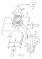
- FIGS. 3 and 4 A typical test probe made in accordance with the present invention is shown in FIGS. 3 and 4.
- the elastomeric connector 10 used in a test probe 39 is preferably assembled as an integral part of a space transformer 44.
- the space transformer serves the purpose of spreading out a closely spaced wiring grid into a more widely spaced wiring grid so that the required circuitry can perform its test operations. Incorporation of the connector 10 built in accordance with the present invention into test probe 39 is easily facilitated and test probe 39 is then mounted on a vertical (2-direction) motion means 40. Referring to FIG.
- the detailed assembly is such that the through hole conductors 16 of the connector 10 contact metal lines 46 of the space transformer 44, which lead to connections 42 which lead to the required test circuitry.
- Elastomeric base 18, through hole conductors 16 and overhanging contact regions 21 are built in accordance with the specifications given for the elastomeric connector built onto the multilayered ceramic substrate as described above, while connections 42 carry the current and signals which are required to test the chips.
- a mechanical vertical motion means 40 is used to raise, lower and hold the test probe in position.
- FIGS. 1 and 2 to follow the operation of the elastomeric connector 10 to provide permanent connections between chips and substrates.
- the elastomeric connector 10 of the present invention When the elastomeric connector 10 of the present invention is in its initial position as shown in FIG. 1, accurate alignment of a dense area array of I/O pads 12 with the connector surface conductor tabs 20 is accomplished as I/O pads 12 contact the relatively large overhanging conductive regions 21 of the surface conductor tabs.
- the connector 10 is built as an integral upper layer upon the top surface of substrate 8.
- the through hole conductors 16 are easily aligned with substrate I/O pads 14 or capture pads 15 by state of the art processing wherein holes are created by lithographic or particle or laser beam processing and filled with solid metal conductors.
- the area of over hanging contact region 21 is approximately 0,015 mm 2.
- the contact area of the chip I/O's is approximately 0,015 mm 2 (i.e. corresponding to a 0,1 mm diameter).
- each 12 square mil I/O pad 12 of chip 9 is aligned with and contacts a 0,015 mm 2 overhanging contact region 21. This result of a ratio of chip I/O pad area to over hanging contact region area of approximately 1 to 2 is a relatively simple task for state of the art positioning equipment.
- the electrical components are biased toward each other and retained together.
- the elastomeric base 18 then exerts a force such that each of the overhanging conductive regions 21 contact and wipe the corresponding I/O pads 12 of chips 9.
- the chips are preferably biased towards the overhang ing conductive regions and retained by flat plate 30, which is preferably a thermal conductor (e.g. metal).
- the biasing force applied by plate 30 onto chips 9, is preferably enough to cause a 25 - 50 percent depression of the elastomer base 18 in the area beneath the interface of chip I/O 12 and overhanging contact region 21, yet not enough to cause any damage to the chip (e.g., less than approximately 180 lbs/square inch).
- biasing force criteria are that in a particular elastomer solid metal system, there is minimal compression to the surface conductor tabs 20 such that the cross sectional area of each surface conductor tab remains constant, and that the elastomer is not punctured at any point.
- a pressure in the range of approximately 0,8 to 3,5 kg/cm 2 preferred to provide the required force is preferred to provide the required force.
- the automatic wiping between the overhanging contact regions 21 of the surface conductor tabs 20 and chip I/O pads 12 is accomplished by contacting chip I/O pads 12 onto overhanging contact region 21 where points A (at the tip of chip I/O 12) and B (corresponding to initial contact point of overhanging contact region 21) initially coincide, causing a downward movement of over hanging contact regions 21.
- points A at the tip of chip I/O 12
- B corresponding to initial contact point of overhanging contact region 21
- the resultant wipe is the distance between points B and B′.
- a 50 percent deformation of the elastomer causes approximately 1 mil of wipe per chip I/O contact, which assures very reliable connections.
- the pressure required to achieve a 25-50 percent deformation is approximately 0,8-3,5 kg/cm 2 the above described system.
- the ability to make high density interconnections of dense area arrays of I/O pads without exerting significant thermal or mechanical stresses on the I/O pads or components being interconnected is a major advance in the VLSI connector art.
- the ability to have automatic wiping of high density area arrays of interconnections is an added advantage that makes such a high density interconnection system practical. Without wiping; reliable, solderless connections cannot be achieved because surface films and debris must be penetrated to minimize contact resistance and assure metal to metal connections.
- the electrical advantages provided by the short inductive path and high conductivity that are provided for in combination with the other advantages afforded by the present invention allows for reliable interconnections that meet the high standards required for state of the art high end VLSI computer systems.
- Another advantage of the present invention relates to its rework capability.
- the standard means of interconnecting chips to substrates currently comprise a bonding means such as soldering or welding, wherein reworking multichip modules causes many strategic problems.
- the means biasing electrical components toward each other must simply be disengaged at room temperature. This is possible because there are no bonding means such as solder incorporated into the present elastomeric interconnection system.
- the presently employed rework methods for solder ball connections require a series of high temperature thermal treatments.
- FIGS. 3 and 4 The operation of the present invention for making temporary connections as part of a test probe is shown in FIGS. 3 and 4.
- an undiced wafer 52 having a plurality of defined chip cites 9A thereon is held in place on a chuck (generally a vacuum chuck) 48, which is mounted on a high precision X-Y table 50.
- the X-Y table moves the chip under the elastomeric connector 10 of test probe 39.
- the elastomeric connector 10 facilitates contact between the test probe and chip.
- the metallized contact pads 12a of the chip come into contact with overhanging contact regions 21.
- a vertical positioning means 40 is used to lower and hold the probe circuitry and elastomeric connector 10 in the required position. Enough pressure is applied by positioning means 40 such that approximately a 25-50% deformation of elastomer 18 under overhanging contact region 21 occurs. This pressure (less than approximately 12 kg/cm 2 ) will be chosen such that it causes the required deformation, yet does not cause any damage to the undiced chips in the wafer. In the present example wherein the elastomer is comprised of approximately 0,125 mm thickness of porous polyurethane and the surface conductor tabs are comprised of approximately 0,05 mm thickness of solid copper, the required pressure is between approximately 0,8 and 3,5 kg/cm 2. Connections 42 provide power and signals, and connect the test probe 10 through the space transformer 44 to the circuitry and equipment (i.e. tester 55) which performs the chip testing.
- the probe After testing of a particular chip location, the probe is raised, the X-Y table is moved to position another chip location, and the testing operation is repeated.
- a preferred method for producing the elastomeric connector 10 of the present invention comprises applying elastomer base 18 to the top surface of electrical component 8 or space transformer 44. Through holes are formed completely through the elastomer layer by laser drilling, E-beam processing, reactive ion etching, or photolithography means so that the resulting array of vias corresponds to the area array of I/O pads on one of the electrical components being connected (i.e., the multichip substrate or tester space transformer). Alternatively, if a preformed elastomer sheet is applied, through holes may be applied to the preformed elastomer prior to joining the elastomer to the substrate or space transformer.
- Solid metal (e.g., copper, Cu/Al) through hole conductors 16 are preferably deposited in the vias through a mask by vapor deposition or plating.
- the surface conductor tabs 20 are then preferably formed by vapor depositing metal onto the top surface of the elastomer through a second mask, or by electroless plating.
- the surface conductor tabs 20 are formed so as to substantially cover and connect to the uppermost exposed surface of the through hole conductors 16 and to simultaneously form overhanging contact regions 21.
- a thin layer of non oxidizing metal, (e.g., gold) is preferably evaporated over the surface conductor tabs.
- the specific elastomer and metals chosen will also depend on factors such as adhesion between the elastomer and metal conductors. Additional steps may be required for enhancing adhesion such as depositing thin layers of adhesion promoting materials such as Cr or Ni or Pd or a combination thereof on the elastomer, and/or metal.
Landscapes
- Engineering & Computer Science (AREA)
- Microelectronics & Electronic Packaging (AREA)
- Physics & Mathematics (AREA)
- General Physics & Mathematics (AREA)
- Wire Bonding (AREA)
- Testing Of Individual Semiconductor Devices (AREA)
- Coupling Device And Connection With Printed Circuit (AREA)
Applications Claiming Priority (2)
| Application Number | Priority Date | Filing Date | Title |
|---|---|---|---|
| US16721388A | 1988-03-11 | 1988-03-11 | |
| US167213 | 1988-03-11 |
Publications (3)
| Publication Number | Publication Date |
|---|---|
| EP0332560A2 true EP0332560A2 (fr) | 1989-09-13 |
| EP0332560A3 EP0332560A3 (en) | 1990-05-02 |
| EP0332560B1 EP0332560B1 (fr) | 1994-03-02 |
Family
ID=22606420
Family Applications (1)
| Application Number | Title | Priority Date | Filing Date |
|---|---|---|---|
| EP89480017A Expired - Lifetime EP0332560B1 (fr) | 1988-03-11 | 1989-01-31 | Connecteurs élastomères pour des composants électroniques et pour des tests |
Country Status (4)
| Country | Link |
|---|---|
| US (1) | US4932883A (fr) |
| EP (1) | EP0332560B1 (fr) |
| JP (1) | JPH0610999B2 (fr) |
| DE (1) | DE68913318T2 (fr) |
Cited By (4)
| Publication number | Priority date | Publication date | Assignee | Title |
|---|---|---|---|---|
| EP0845677A1 (fr) * | 1996-11-08 | 1998-06-03 | W.L. GORE & ASSOCIATES, INC. | Méthode d'utilisation d'un matériau temporaire conducteur suivant l'axe-z |
| EP0841572A3 (fr) * | 1996-11-08 | 1998-07-08 | W.L. GORE & ASSOCIATES, INC. | Système de déverminage de pastille |
| WO1999021227A1 (fr) * | 1997-10-17 | 1999-04-29 | Molex Incorporated | Ensemble connecteur pour le logement de composants du type bga |
| FR2949027A1 (fr) * | 2009-08-10 | 2011-02-11 | Bosch Gmbh Robert | Dispositif de liaison pour realiser une liaison mecanique et electrique d'un composant, notamment d'un moteur electrique |
Families Citing this family (56)
| Publication number | Priority date | Publication date | Assignee | Title |
|---|---|---|---|---|
| US5071359A (en) | 1990-04-27 | 1991-12-10 | Rogers Corporation | Array connector |
| US5245751A (en) | 1990-04-27 | 1993-09-21 | Circuit Components, Incorporated | Array connector |
| US5342807A (en) * | 1991-06-04 | 1994-08-30 | Micron Technology, Inc. | Soft bond for semiconductor dies |
| US5336649A (en) * | 1991-06-04 | 1994-08-09 | Micron Technology, Inc. | Removable adhesives for attachment of semiconductor dies |
| US5259781A (en) * | 1992-11-18 | 1993-11-09 | International Business Machines Corporation | Electrical connector alignment and actuation assembly |
| US5442852A (en) * | 1993-10-26 | 1995-08-22 | Pacific Microelectronics Corporation | Method of fabricating solder ball array |
| US5434452A (en) * | 1993-11-01 | 1995-07-18 | Motorola, Inc. | Z-axis compliant mechanical IC wiring substrate and method for making the same |
| US6246247B1 (en) | 1994-11-15 | 2001-06-12 | Formfactor, Inc. | Probe card assembly and kit, and methods of using same |
| US6624648B2 (en) | 1993-11-16 | 2003-09-23 | Formfactor, Inc. | Probe card assembly |
| US20020053734A1 (en) | 1993-11-16 | 2002-05-09 | Formfactor, Inc. | Probe card assembly and kit, and methods of making same |
| US7073254B2 (en) | 1993-11-16 | 2006-07-11 | Formfactor, Inc. | Method for mounting a plurality of spring contact elements |
| US6741085B1 (en) * | 1993-11-16 | 2004-05-25 | Formfactor, Inc. | Contact carriers (tiles) for populating larger substrates with spring contacts |
| US5800184A (en) * | 1994-03-08 | 1998-09-01 | International Business Machines Corporation | High density electrical interconnect apparatus and method |
| US5563470A (en) * | 1994-08-31 | 1996-10-08 | Cornell Research Foundation, Inc. | Tiled panel display assembly |
| WO1996009645A1 (fr) * | 1994-09-20 | 1996-03-28 | Hitachi, Ltd. | Composant a semiconducteurs et sa structure de montage |
| AU5937096A (en) * | 1995-07-07 | 1997-02-10 | Minnesota Mining And Manufacturing Company | Separable electrical connector assembly having a planar array of conductive protrusions |
| US5691041A (en) * | 1995-09-29 | 1997-11-25 | International Business Machines Corporation | Socket for semi-permanently connecting a solder ball grid array device using a dendrite interposer |
| US6483328B1 (en) * | 1995-11-09 | 2002-11-19 | Formfactor, Inc. | Probe card for probing wafers with raised contact elements |
| US8033838B2 (en) | 1996-02-21 | 2011-10-11 | Formfactor, Inc. | Microelectronic contact structure |
| US6403226B1 (en) | 1996-05-17 | 2002-06-11 | 3M Innovative Properties Company | Electronic assemblies with elastomeric members made from cured, room temperature curable silicone compositions having improved stress relaxation resistance |
| US5874319A (en) * | 1996-05-21 | 1999-02-23 | Honeywell Inc. | Vacuum die bond for known good die assembly |
| SG71046A1 (en) | 1996-10-10 | 2000-03-21 | Connector Systems Tech Nv | High density connector and method of manufacture |
| US6018584A (en) * | 1996-11-06 | 2000-01-25 | Motorola, Inc. | Electronic component assembly for an electronic device and method of assembling the same |
| US5828226A (en) * | 1996-11-06 | 1998-10-27 | Cerprobe Corporation | Probe card assembly for high density integrated circuits |
| DE19752834A1 (de) * | 1997-11-28 | 1999-06-02 | Bosch Gmbh Robert | Kraftstoffeinspritzeinrichtung für Brennkraftmaschinen |
| JPH11329648A (ja) * | 1998-05-19 | 1999-11-30 | Molex Inc | Icデバイスソケット |
| US6027346A (en) * | 1998-06-29 | 2000-02-22 | Xandex, Inc. | Membrane-supported contactor for semiconductor test |
| US6227901B1 (en) | 1998-07-10 | 2001-05-08 | Thomas & Betts International, Inc. | Motor boot for a circuit board |
| US6595408B1 (en) * | 1998-10-07 | 2003-07-22 | Micron Technology, Inc. | Method of attaching solder balls to BGA package utilizing a tool to pick and dip the solder ball in flux prior to placement |
| US6268275B1 (en) | 1998-10-08 | 2001-07-31 | Micron Technology, Inc. | Method of locating conductive spheres utilizing screen and hopper of solder balls |
| US6137297A (en) * | 1999-01-06 | 2000-10-24 | Vertest Systemsn Corp. | Electronic test probe interface assembly and method of manufacture |
| US6559388B1 (en) | 1999-06-08 | 2003-05-06 | International Business Machines Corporation | Strain relief for substrates having a low coefficient of thermal expansion |
| US6628136B2 (en) * | 1999-09-02 | 2003-09-30 | Micron Technology, Inc. | Method and apparatus for testing a semiconductor package |
| US6734688B1 (en) | 2000-05-15 | 2004-05-11 | Teradyne, Inc. | Low compliance tester interface |
| DE10028184A1 (de) * | 2000-06-09 | 2002-03-07 | Hirschmann Austria Gmbh Rankwe | Vorrichtung zum Verbindung von elektrischen Leitern |
| US6570396B1 (en) | 2000-11-24 | 2003-05-27 | Kulicke & Soffa Investment, Inc. | Interface structure for contacting probe beams |
| TW525273B (en) * | 2002-02-07 | 2003-03-21 | Via Tech Inc | Elastomer interposer for fixing package onto printed circuit board and fabrication method thereof |
| US7503768B2 (en) * | 2003-11-05 | 2009-03-17 | Tensolite Company | High frequency connector assembly |
| US7074047B2 (en) * | 2003-11-05 | 2006-07-11 | Tensolite Company | Zero insertion force high frequency connector |
| US7404718B2 (en) * | 2003-11-05 | 2008-07-29 | Tensolite Company | High frequency connector assembly |
| KR100674440B1 (ko) * | 2005-08-12 | 2007-01-25 | 주식회사 파이컴 | 프로브 카드 제조 방법 및 장치 |
| US7452214B2 (en) * | 2006-12-08 | 2008-11-18 | Verigy (Singapore) Pte. Ltd. | Interconnect assemblies, and methods of forming interconnects, between conductive contact bumps and conductive contact pads |
| US8092246B1 (en) | 2008-04-18 | 2012-01-10 | Lockheed Martin Corporation | Self-locking micro-D connector |
| TWI368743B (en) * | 2008-11-04 | 2012-07-21 | King Yuan Electronics Co Ltd | Probe card assembly and probes therein |
| JP5943742B2 (ja) * | 2012-07-04 | 2016-07-05 | 三菱電機株式会社 | 半導体試験治具およびそれを用いた半導体試験方法 |
| TWI490508B (zh) * | 2012-12-17 | 2015-07-01 | 巨擘科技股份有限公司 | 軟性測試裝置及其測試方法 |
| TWI643725B (zh) | 2016-02-24 | 2018-12-11 | 耐克創新有限合夥公司 | 真空輔助切割工具,使用其的焊接系統以及使用真空輔助切割工具進行製造的方法 |
| US10120020B2 (en) | 2016-06-16 | 2018-11-06 | Formfactor Beaverton, Inc. | Probe head assemblies and probe systems for testing integrated circuit devices |
| JP2018067483A (ja) * | 2016-10-20 | 2018-04-26 | ヤマハ株式会社 | 異方導電性シート、電気検査ヘッド、電気検査装置及び異方導電性シートの製造方法 |
| WO2019022942A1 (fr) | 2017-07-24 | 2019-01-31 | Cerebras Systems Inc. | Appareil et procédé de fixation de substrats avec des coefficients de dilatation thermique variables |
| US10366967B2 (en) | 2017-07-24 | 2019-07-30 | Cerebras Systems Inc. | Apparatus and method for multi-die interconnection |
| WO2019040273A1 (fr) | 2017-08-24 | 2019-02-28 | Cerebras Systems Inc. | Appareil et procédé de fixation de composants d'un circuit intégré |
| US10840216B2 (en) | 2019-03-05 | 2020-11-17 | Cerebras Systems Inc. | Systems and methods for powering an integrated circuit having multiple interconnected die |
| US11145530B2 (en) | 2019-11-08 | 2021-10-12 | Cerebras Systems Inc. | System and method for alignment of an integrated circuit |
| CN116746007A (zh) * | 2020-12-11 | 2023-09-12 | 三井化学株式会社 | 各向异性导电片及电气检查方法 |
| CN118501673A (zh) * | 2024-07-18 | 2024-08-16 | 宁波吉品科技有限公司 | 一种基于压电陶瓷的芯片集成测试板 |
Family Cites Families (17)
| Publication number | Priority date | Publication date | Assignee | Title |
|---|---|---|---|---|
| US3683105A (en) * | 1970-10-13 | 1972-08-08 | Westinghouse Electric Corp | Microcircuit modular package |
| US3904934A (en) * | 1973-03-26 | 1975-09-09 | Massachusetts Inst Technology | Interconnection of planar electronic structures |
| US3967162A (en) * | 1974-07-24 | 1976-06-29 | Amp Incorporated | Interconnection of oppositely disposed circuit devices |
| US4008300A (en) * | 1974-10-15 | 1977-02-15 | A & P Products Incorporated | Multi-conductor element and method of making same |
| US4038599A (en) * | 1974-12-30 | 1977-07-26 | International Business Machines Corporation | High density wafer contacting and test system |
| US4003621A (en) * | 1975-06-16 | 1977-01-18 | Technical Wire Products, Inc. | Electrical connector employing conductive rectilinear elements |
| US3993123A (en) * | 1975-10-28 | 1976-11-23 | International Business Machines Corporation | Gas encapsulated cooling module |
| JPS5555985U (fr) * | 1978-10-12 | 1980-04-16 | ||
| US4249302A (en) * | 1978-12-28 | 1981-02-10 | Ncr Corporation | Multilayer printed circuit board |
| JPS568081U (fr) * | 1979-06-29 | 1981-01-23 | ||
| US4443756A (en) * | 1980-11-25 | 1984-04-17 | Lightbody James D | Apparatus and method for testing circuit boards |
| US4373778A (en) * | 1980-12-30 | 1983-02-15 | International Business Machines Corporation | Connector implemented with fiber optic means and site therein for integrated circuit chips |
| US4548451A (en) * | 1984-04-27 | 1985-10-22 | International Business Machines Corporation | Pinless connector interposer and method for making the same |
| JPS6139468A (ja) * | 1984-07-31 | 1986-02-25 | 日本黒鉛工業株式会社 | 可撓性スルホ−ル両面ヒ−トシ−ルコネクタ及びその製造方法 |
| JPS61133586A (ja) * | 1984-11-30 | 1986-06-20 | 信越ポリマ−株式会社 | コネクタ− |
| US4778950A (en) * | 1985-07-22 | 1988-10-18 | Digital Equipment Corporation | Anisotropic elastomeric interconnecting system |
| JPS6230367U (fr) * | 1985-08-07 | 1987-02-24 |
-
1989
- 1989-01-31 DE DE68913318T patent/DE68913318T2/de not_active Expired - Fee Related
- 1989-01-31 EP EP89480017A patent/EP0332560B1/fr not_active Expired - Lifetime
- 1989-02-20 JP JP1038542A patent/JPH0610999B2/ja not_active Expired - Lifetime
- 1989-07-20 US US07/384,089 patent/US4932883A/en not_active Expired - Fee Related
Cited By (5)
| Publication number | Priority date | Publication date | Assignee | Title |
|---|---|---|---|---|
| EP0845677A1 (fr) * | 1996-11-08 | 1998-06-03 | W.L. GORE & ASSOCIATES, INC. | Méthode d'utilisation d'un matériau temporaire conducteur suivant l'axe-z |
| EP0841572A3 (fr) * | 1996-11-08 | 1998-07-08 | W.L. GORE & ASSOCIATES, INC. | Système de déverminage de pastille |
| US5966022A (en) * | 1996-11-08 | 1999-10-12 | W. L. Gore & Associates, Inc. | Wafer level burn-in system |
| WO1999021227A1 (fr) * | 1997-10-17 | 1999-04-29 | Molex Incorporated | Ensemble connecteur pour le logement de composants du type bga |
| FR2949027A1 (fr) * | 2009-08-10 | 2011-02-11 | Bosch Gmbh Robert | Dispositif de liaison pour realiser une liaison mecanique et electrique d'un composant, notamment d'un moteur electrique |
Also Published As
| Publication number | Publication date |
|---|---|
| EP0332560B1 (fr) | 1994-03-02 |
| EP0332560A3 (en) | 1990-05-02 |
| DE68913318T2 (de) | 1994-09-15 |
| JPH0610999B2 (ja) | 1994-02-09 |
| JPH01255176A (ja) | 1989-10-12 |
| US4932883A (en) | 1990-06-12 |
| DE68913318D1 (de) | 1994-04-07 |
Similar Documents
| Publication | Publication Date | Title |
|---|---|---|
| EP0332560B1 (fr) | Connecteurs élastomères pour des composants électroniques et pour des tests | |
| US6029344A (en) | Composite interconnection element for microelectronic components, and method of making same | |
| US5806181A (en) | Contact carriers (tiles) for populating larger substrates with spring contacts | |
| KR100324059B1 (ko) | 초소형 전자 부품용 상호 접속 요소 | |
| EP0886894B1 (fr) | Supports de contacts a ressorts places sur des substrats | |
| US6224396B1 (en) | Compliant, surface-mountable interposer | |
| US6286208B1 (en) | Interconnector with contact pads having enhanced durability | |
| US5565280A (en) | Electrical interconnect using particle enhanced joining of metal surfaces | |
| US6741085B1 (en) | Contact carriers (tiles) for populating larger substrates with spring contacts | |
| US5414298A (en) | Semiconductor chip assemblies and components with pressure contact | |
| JP3006885B2 (ja) | 相互接続のためのコンタクト構造、介在体、半導体アセンブリおよび方法 | |
| US5430614A (en) | Electrical interconnect using particle enhanced joining of metal surfaces | |
| EP0764352B1 (fr) | Contacts et assemblages microelectroniques | |
| US7501839B2 (en) | Interposer and test assembly for testing electronic devices | |
| EP0792462B1 (fr) | Carte a sondes et son procede d'utilisation | |
| EP0792519A1 (fr) | Elements d'interconnexion composite pour composants micro-electroniques | |
| KR100278342B1 (ko) | 탐침 카드 조립체에서 탐침 요소의 배향을 변경하는 방법 |
Legal Events
| Date | Code | Title | Description |
|---|---|---|---|
| PUAI | Public reference made under article 153(3) epc to a published international application that has entered the european phase |
Free format text: ORIGINAL CODE: 0009012 |
|
| AK | Designated contracting states |
Kind code of ref document: A2 Designated state(s): DE FR GB |
|
| PUAL | Search report despatched |
Free format text: ORIGINAL CODE: 0009013 |
|
| 17P | Request for examination filed |
Effective date: 19900120 |
|
| AK | Designated contracting states |
Kind code of ref document: A3 Designated state(s): DE FR GB |
|
| 17Q | First examination report despatched |
Effective date: 19920701 |
|
| GRAA | (expected) grant |
Free format text: ORIGINAL CODE: 0009210 |
|
| AK | Designated contracting states |
Kind code of ref document: B1 Designated state(s): DE FR GB |
|
| REF | Corresponds to: |
Ref document number: 68913318 Country of ref document: DE Date of ref document: 19940407 |
|
| ET | Fr: translation filed | ||
| PGFP | Annual fee paid to national office [announced via postgrant information from national office to epo] |
Ref country code: FR Payment date: 19941223 Year of fee payment: 7 |
|
| PLBE | No opposition filed within time limit |
Free format text: ORIGINAL CODE: 0009261 |
|
| STAA | Information on the status of an ep patent application or granted ep patent |
Free format text: STATUS: NO OPPOSITION FILED WITHIN TIME LIMIT |
|
| PGFP | Annual fee paid to national office [announced via postgrant information from national office to epo] |
Ref country code: DE Payment date: 19950117 Year of fee payment: 7 |
|
| 26N | No opposition filed | ||
| PGFP | Annual fee paid to national office [announced via postgrant information from national office to epo] |
Ref country code: GB Payment date: 19951215 Year of fee payment: 8 |
|
| PG25 | Lapsed in a contracting state [announced via postgrant information from national office to epo] |
Ref country code: FR Effective date: 19960930 |
|
| PG25 | Lapsed in a contracting state [announced via postgrant information from national office to epo] |
Ref country code: DE Effective date: 19961001 |
|
| REG | Reference to a national code |
Ref country code: FR Ref legal event code: ST |
|
| PG25 | Lapsed in a contracting state [announced via postgrant information from national office to epo] |
Ref country code: GB Effective date: 19970131 |
|
| GBPC | Gb: european patent ceased through non-payment of renewal fee |
Effective date: 19970131 |