EP0334381B1 - Beschichtungsfilm enthaltend eine negativ arbeitende lichtempfindliche Zusammensetzung und Bilderzeugungsverfahren - Google Patents
Beschichtungsfilm enthaltend eine negativ arbeitende lichtempfindliche Zusammensetzung und Bilderzeugungsverfahren Download PDFInfo
- Publication number
- EP0334381B1 EP0334381B1 EP89105301A EP89105301A EP0334381B1 EP 0334381 B1 EP0334381 B1 EP 0334381B1 EP 89105301 A EP89105301 A EP 89105301A EP 89105301 A EP89105301 A EP 89105301A EP 0334381 B1 EP0334381 B1 EP 0334381B1
- Authority
- EP
- European Patent Office
- Prior art keywords
- coating film
- pattern
- photosensitive composition
- wavelength
- light
- Prior art date
- Legal status (The legal status is an assumption and is not a legal conclusion. Google has not performed a legal analysis and makes no representation as to the accuracy of the status listed.)
- Expired - Lifetime
Links
- 239000011248 coating agent Substances 0.000 title claims description 40
- 238000000576 coating method Methods 0.000 title claims description 40
- 239000000203 mixture Substances 0.000 title claims description 21
- 238000000034 method Methods 0.000 title claims description 18
- 230000007261 regionalization Effects 0.000 title claims description 8
- 238000002835 absorbance Methods 0.000 claims description 20
- 150000001875 compounds Chemical class 0.000 claims description 18
- -1 aromatic azide compound Chemical class 0.000 claims description 16
- 229920000642 polymer Polymers 0.000 claims description 14
- 239000000758 substrate Substances 0.000 claims description 12
- 230000018109 developmental process Effects 0.000 claims description 8
- WLNIECNLFRHWOI-UHFFFAOYSA-N [[4-(4-diazonioimino-3-methoxycyclohexa-2,5-dien-1-ylidene)-2-methoxycyclohexa-2,5-dien-1-ylidene]hydrazinylidene]azanide Chemical group C1=C(N=[N+]=[N-])C(OC)=CC(C=2C=C(OC)C(N=[N+]=[N-])=CC=2)=C1 WLNIECNLFRHWOI-UHFFFAOYSA-N 0.000 claims description 7
- 239000011347 resin Substances 0.000 claims description 6
- 229920005989 resin Polymers 0.000 claims description 6
- JESXATFQYMPTNL-UHFFFAOYSA-N mono-hydroxyphenyl-ethylene Natural products OC1=CC=CC=C1C=C JESXATFQYMPTNL-UHFFFAOYSA-N 0.000 claims description 4
- DVSWAJXDQPJJLT-UHFFFAOYSA-N 1-azido-2-methyl-4-nitrobenzene Chemical compound CC1=CC([N+]([O-])=O)=CC=C1N=[N+]=[N-] DVSWAJXDQPJJLT-UHFFFAOYSA-N 0.000 claims description 3
- LHCUYYJTVIYFEQ-UHFFFAOYSA-N 1-azido-3-(3-azidophenyl)sulfonylbenzene Chemical compound [N-]=[N+]=NC1=CC=CC(S(=O)(=O)C=2C=C(C=CC=2)N=[N+]=[N-])=C1 LHCUYYJTVIYFEQ-UHFFFAOYSA-N 0.000 claims description 3
- QTWJRLJHJPIABL-UHFFFAOYSA-N 2-methylphenol;3-methylphenol;4-methylphenol Chemical compound CC1=CC=C(O)C=C1.CC1=CC=CC(O)=C1.CC1=CC=CC=C1O QTWJRLJHJPIABL-UHFFFAOYSA-N 0.000 claims description 3
- XLLXMBCBJGATSP-UHFFFAOYSA-N 2-phenylethenol Chemical compound OC=CC1=CC=CC=C1 XLLXMBCBJGATSP-UHFFFAOYSA-N 0.000 claims description 3
- 229920001577 copolymer Polymers 0.000 claims description 3
- 229930003836 cresol Natural products 0.000 claims description 3
- 229920003986 novolac Polymers 0.000 claims description 3
- 230000005855 radiation Effects 0.000 claims 1
- 239000000047 product Substances 0.000 description 20
- 230000035945 sensitivity Effects 0.000 description 15
- 229920002120 photoresistant polymer Polymers 0.000 description 13
- 238000002834 transmittance Methods 0.000 description 11
- UHOVQNZJYSORNB-UHFFFAOYSA-N Benzene Chemical compound C1=CC=CC=C1 UHOVQNZJYSORNB-UHFFFAOYSA-N 0.000 description 6
- 230000031700 light absorption Effects 0.000 description 4
- 230000010355 oscillation Effects 0.000 description 4
- WGTYBPLFGIVFAS-UHFFFAOYSA-M tetramethylammonium hydroxide Chemical compound [OH-].C[N+](C)(C)C WGTYBPLFGIVFAS-UHFFFAOYSA-M 0.000 description 4
- XUIMIQQOPSSXEZ-UHFFFAOYSA-N Silicon Chemical compound [Si] XUIMIQQOPSSXEZ-UHFFFAOYSA-N 0.000 description 3
- 238000004519 manufacturing process Methods 0.000 description 3
- 239000000463 material Substances 0.000 description 3
- 229920003229 poly(methyl methacrylate) Polymers 0.000 description 3
- 239000004926 polymethyl methacrylate Substances 0.000 description 3
- 239000004065 semiconductor Substances 0.000 description 3
- 229910052710 silicon Inorganic materials 0.000 description 3
- 239000010703 silicon Substances 0.000 description 3
- XLYOFNOQVPJJNP-UHFFFAOYSA-N water Substances O XLYOFNOQVPJJNP-UHFFFAOYSA-N 0.000 description 3
- LFQSCWFLJHTTHZ-UHFFFAOYSA-N Ethanol Chemical compound CCO LFQSCWFLJHTTHZ-UHFFFAOYSA-N 0.000 description 2
- VEXZGXHMUGYJMC-UHFFFAOYSA-N Hydrochloric acid Chemical compound Cl VEXZGXHMUGYJMC-UHFFFAOYSA-N 0.000 description 2
- PXIPVTKHYLBLMZ-UHFFFAOYSA-N Sodium azide Chemical compound [Na+].[N-]=[N+]=[N-] PXIPVTKHYLBLMZ-UHFFFAOYSA-N 0.000 description 2
- 238000010521 absorption reaction Methods 0.000 description 2
- 230000015572 biosynthetic process Effects 0.000 description 2
- 230000000052 comparative effect Effects 0.000 description 2
- 238000001816 cooling Methods 0.000 description 2
- JHIVVAPYMSGYDF-UHFFFAOYSA-N cyclohexanone Chemical compound O=C1CCCCC1 JHIVVAPYMSGYDF-UHFFFAOYSA-N 0.000 description 2
- 230000003247 decreasing effect Effects 0.000 description 2
- 238000001312 dry etching Methods 0.000 description 2
- 230000010354 integration Effects 0.000 description 2
- 150000002989 phenols Chemical class 0.000 description 2
- LPXPTNMVRIOKMN-UHFFFAOYSA-M sodium nitrite Chemical compound [Na+].[O-]N=O LPXPTNMVRIOKMN-UHFFFAOYSA-M 0.000 description 2
- ZMPZWXKBGSQATE-UHFFFAOYSA-N 3-(4-aminophenyl)sulfonylaniline Chemical compound C1=CC(N)=CC=C1S(=O)(=O)C1=CC=CC(N)=C1 ZMPZWXKBGSQATE-UHFFFAOYSA-N 0.000 description 1
- 230000010748 Photoabsorption Effects 0.000 description 1
- 206010070834 Sensitisation Diseases 0.000 description 1
- JWNBYUSSORDWOT-UHFFFAOYSA-N [Kr]Cl Chemical compound [Kr]Cl JWNBYUSSORDWOT-UHFFFAOYSA-N 0.000 description 1
- VZPPHXVFMVZRTE-UHFFFAOYSA-N [Kr]F Chemical compound [Kr]F VZPPHXVFMVZRTE-UHFFFAOYSA-N 0.000 description 1
- ISQINHMJILFLAQ-UHFFFAOYSA-N argon hydrofluoride Chemical compound F.[Ar] ISQINHMJILFLAQ-UHFFFAOYSA-N 0.000 description 1
- 125000003118 aryl group Chemical group 0.000 description 1
- 239000007859 condensation product Substances 0.000 description 1
- 239000000470 constituent Substances 0.000 description 1
- 238000004132 cross linking Methods 0.000 description 1
- 239000013078 crystal Substances 0.000 description 1
- 238000000276 deep-ultraviolet lithography Methods 0.000 description 1
- 230000007547 defect Effects 0.000 description 1
- 230000000694 effects Effects 0.000 description 1
- 238000005530 etching Methods 0.000 description 1
- 239000000706 filtrate Substances 0.000 description 1
- 238000005187 foaming Methods 0.000 description 1
- 238000002844 melting Methods 0.000 description 1
- 230000008018 melting Effects 0.000 description 1
- WSFSSNUMVMOOMR-NJFSPNSNSA-N methanone Chemical compound O=[14CH2] WSFSSNUMVMOOMR-NJFSPNSNSA-N 0.000 description 1
- 230000003287 optical effect Effects 0.000 description 1
- 229920001568 phenolic resin Polymers 0.000 description 1
- 239000005011 phenolic resin Substances 0.000 description 1
- 239000002244 precipitate Substances 0.000 description 1
- 150000003839 salts Chemical class 0.000 description 1
- 230000008313 sensitization Effects 0.000 description 1
- 238000004904 shortening Methods 0.000 description 1
- 239000002356 single layer Substances 0.000 description 1
- 235000010288 sodium nitrite Nutrition 0.000 description 1
- 230000003595 spectral effect Effects 0.000 description 1
- 238000004528 spin coating Methods 0.000 description 1
- 238000003756 stirring Methods 0.000 description 1
- 239000000126 substance Substances 0.000 description 1
- 238000003786 synthesis reaction Methods 0.000 description 1
- 238000010189 synthetic method Methods 0.000 description 1
- HGCGQDMQKGRJNO-UHFFFAOYSA-N xenon monochloride Chemical compound [Xe]Cl HGCGQDMQKGRJNO-UHFFFAOYSA-N 0.000 description 1
Images

Classifications
-
- G—PHYSICS
- G03—PHOTOGRAPHY; CINEMATOGRAPHY; ANALOGOUS TECHNIQUES USING WAVES OTHER THAN OPTICAL WAVES; ELECTROGRAPHY; HOLOGRAPHY
- G03F—PHOTOMECHANICAL PRODUCTION OF TEXTURED OR PATTERNED SURFACES, e.g. FOR PRINTING, FOR PROCESSING OF SEMICONDUCTOR DEVICES; MATERIALS THEREFOR; ORIGINALS THEREFOR; APPARATUS SPECIALLY ADAPTED THEREFOR
- G03F7/00—Photomechanical, e.g. photolithographic, production of textured or patterned surfaces, e.g. printing surfaces; Materials therefor, e.g. comprising photoresists; Apparatus specially adapted therefor
- G03F7/004—Photosensitive materials
-
- G—PHYSICS
- G03—PHOTOGRAPHY; CINEMATOGRAPHY; ANALOGOUS TECHNIQUES USING WAVES OTHER THAN OPTICAL WAVES; ELECTROGRAPHY; HOLOGRAPHY
- G03F—PHOTOMECHANICAL PRODUCTION OF TEXTURED OR PATTERNED SURFACES, e.g. FOR PRINTING, FOR PROCESSING OF SEMICONDUCTOR DEVICES; MATERIALS THEREFOR; ORIGINALS THEREFOR; APPARATUS SPECIALLY ADAPTED THEREFOR
- G03F7/00—Photomechanical, e.g. photolithographic, production of textured or patterned surfaces, e.g. printing surfaces; Materials therefor, e.g. comprising photoresists; Apparatus specially adapted therefor
- G03F7/004—Photosensitive materials
- G03F7/008—Azides
Definitions
- MP2400 has an absorbance at 248 nm of 0.46, which is rather large for a positive type photoresist. Therefore, incident light does not reach the lower part of photoresist sufficiently, so that the cross section of a pattern of MP2400 has a considerably undesirable shape, i.e., an undercut shape.
- PMMA absorbs light too weakly, hence it has a sensitivity of as low as 32 J/cm which is disadvantageous for practical use.
- PMMA has a defect in that when it is used on a silicon wafer, 80% or more of incident light reaches the silicon wafer substrate and therefore a large standing wave is raised, so that a fine pattern cannot be resolved.
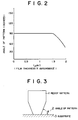
- Fig. 3 illustrates the definition of the angle of the resist pattern of the present invention.
Landscapes
- Physics & Mathematics (AREA)
- General Physics & Mathematics (AREA)
- Exposure And Positioning Against Photoresist Photosensitive Materials (AREA)
- Materials For Photolithography (AREA)
Claims (4)
- Überzugschicht, hergestellt aus einer negativ kopierenden, photosensitiven Zusammensetzung, die im wesentlichen aus mindestens einer aromatischen Azidverbindung, die ausgewählt ist aus der Gruppe 4,4'-Diazido-3,3'-dimethoxybiphenyl, 3,3'-Diazidodiphenylsulfon, 4-Nitro-2-methylphenyl-azid und 3,4'-Diazidodiphenylsulfon, und einer in Alkali löslichen Polymerverbindung besteht, dadurch gekennzeichnet, daß die Extinktion bei einer Bestrahlung der Überzugschicht mit einer Dicke von 1 µm bei einer Wellenlänge von 248 nm 0,5 bis 1,5 beträgt.
- Überzugschicht gemäß Anspruch 1, wobei die in Alkali lösliche Polymerverbindung eines von den Cresol-Novolak-harzen, Phenol-Copolymeren, Hydroxystyrol oder HydroxystyrolCopolymeren ist.
- Überzugschicht gemäß Anspruch 1 oder 2, wobei die aromatische Azidverbindung 5 bis 30 Gew.-% des Gesamtgewichts der aromatischen Azidverbindung und der in Alkali löslichen Polymerverbindung ausmacht.
- Verfahren zur Herstellung einer Musterstruktur mit der Überzugschicht, die aus einer negativ kopierenden, photosensitiven Zusammensetzung gemäß einem der Ansprüche 1 bis 3 besteht, gekennzeichnet durch die SchritteAufbringen der Zusammensetzung auf dem Substrat, um eine Überzugschicht zu bilden,Bestrahlen der Überzugschicht mit einem Strahl aus einer KrF-Excimerlaserquelle, um ein vorbestimmtes negatives Muster aufzudrucken, undAusbilden des vorbestimmten negativen Musters durch Entwickeln.
Applications Claiming Priority (2)
| Application Number | Priority Date | Filing Date | Title |
|---|---|---|---|
| JP63069082A JP2643261B2 (ja) | 1988-03-23 | 1988-03-23 | ネガ型感光性組成物及びパタン形成方法 |
| JP69082/88 | 1988-03-23 |
Publications (3)
| Publication Number | Publication Date |
|---|---|
| EP0334381A2 EP0334381A2 (de) | 1989-09-27 |
| EP0334381A3 EP0334381A3 (en) | 1990-10-10 |
| EP0334381B1 true EP0334381B1 (de) | 1996-02-14 |
Family
ID=13392309
Family Applications (1)
| Application Number | Title | Priority Date | Filing Date |
|---|---|---|---|
| EP89105301A Expired - Lifetime EP0334381B1 (de) | 1988-03-23 | 1989-03-23 | Beschichtungsfilm enthaltend eine negativ arbeitende lichtempfindliche Zusammensetzung und Bilderzeugungsverfahren |
Country Status (4)
| Country | Link |
|---|---|
| EP (1) | EP0334381B1 (de) |
| JP (1) | JP2643261B2 (de) |
| KR (1) | KR890015072A (de) |
| DE (1) | DE68925655T2 (de) |
Families Citing this family (4)
| Publication number | Priority date | Publication date | Assignee | Title |
|---|---|---|---|---|
| WO1993012055A2 (en) * | 1991-12-10 | 1993-06-24 | The Dow Chemical Company | Photocurable cyclobutarene compositions |
| US5854302A (en) * | 1993-04-29 | 1998-12-29 | The Dow Chemical Company | Partially polymerized divinylsiloxane linked bisbenzocyclobutene resins and methods for making said resins |
| CA2106231A1 (en) * | 1993-09-15 | 1995-03-16 | Sambasivan Venkat Eswaran | Negative photoresist and a process therefor |
| CN108347911B (zh) * | 2015-10-21 | 2019-10-08 | 纯钓日本公司 | 渔线轮 |
-
1988
- 1988-03-23 JP JP63069082A patent/JP2643261B2/ja not_active Expired - Lifetime
-
1989
- 1989-03-20 KR KR1019890003455A patent/KR890015072A/ko not_active Ceased
- 1989-03-23 DE DE68925655T patent/DE68925655T2/de not_active Expired - Fee Related
- 1989-03-23 EP EP89105301A patent/EP0334381B1/de not_active Expired - Lifetime
Also Published As
| Publication number | Publication date |
|---|---|
| KR890015072A (ko) | 1989-10-28 |
| EP0334381A2 (de) | 1989-09-27 |
| DE68925655D1 (de) | 1996-03-28 |
| EP0334381A3 (en) | 1990-10-10 |
| JPH01241543A (ja) | 1989-09-26 |
| DE68925655T2 (de) | 1996-09-19 |
| JP2643261B2 (ja) | 1997-08-20 |
Similar Documents
| Publication | Publication Date | Title |
|---|---|---|
| KR100268292B1 (ko) | 혼성포토레지스트조성물과그제조방법상기조성물을이용한집적회로칩의제조방법및이방법에의해제조된집적회로칩 | |
| EP0045639B1 (de) | Verfahren zum Herstellen eines mikroskopischen Musters | |
| US4968581A (en) | High resolution photoresist of imide containing polymers | |
| EP0982628B1 (de) | Chemisch verstärkte Positivresistzusammensetzung | |
| KR0163953B1 (ko) | 포지티브형 감방사선 혼합물 및 이로부터 제조된 감방사선 복사물질 | |
| EP1240553B1 (de) | Photoresistzusammensetzung für die belichtung mit duv-strahlung | |
| KR100383471B1 (ko) | 방사선감수성조성물 | |
| JPH04219757A (ja) | 感放射線性混合物 | |
| DE69032077T2 (de) | Fotoresist für nahes U.V. | |
| EP0681713A1 (de) | Sulfonsäureester, damit hergestellte strahlungsempfindliche gemische und deren verwendung | |
| US4912018A (en) | High resolution photoresist based on imide containing polymers | |
| JPH05281745A (ja) | 放射線感応性混合物及びレリーフ構造の製造方法 | |
| US4614706A (en) | Method of forming a microscopic pattern with far UV pattern exposure, alkaline solution development, and dry etching | |
| US4985344A (en) | Radiation imaging process for forming pattern without alkali-soluble polymer underlayer and water soluble radiation-sensitive diazonium salt overlayer | |
| US5401608A (en) | Negative-working radiation-sensitive mixture and radiation-sensitive recording material produced therewith | |
| US6014422A (en) | Method for varying x-ray hybrid resist space dimensions | |
| US6120977A (en) | Photoresist with bleaching effect | |
| EP0917000A2 (de) | Positivphotoresistzusammensetzung und Verfahren zur Herstellung eines Resistmusters | |
| JPH08262720A (ja) | 可塑剤を含む放射線感応性組成物 | |
| EP0334381A2 (de) | Beschichtungsfilm enthaltend eine negativ arbeitende lichtempfindliche Zusammensetzung und Bilderzeugungsverfahren | |
| JP3453392B2 (ja) | 酸硬化フォトレジスト | |
| EP0440376B1 (de) | Verfahren zur Herstellung einer Bildstruktur | |
| US5846689A (en) | Positive-working radiation-sensitive mixture and production of relief structures | |
| EP0766141B1 (de) | Verfahren zur Erzeugung eines Musters | |
| GB2079481A (en) | Method for the formation of surface relief patterns using deep ultraviolet radiation exposure of resist composition |
Legal Events
| Date | Code | Title | Description |
|---|---|---|---|
| PUAI | Public reference made under article 153(3) epc to a published international application that has entered the european phase |
Free format text: ORIGINAL CODE: 0009012 |
|
| AK | Designated contracting states |
Kind code of ref document: A2 Designated state(s): DE FR NL |
|
| PUAL | Search report despatched |
Free format text: ORIGINAL CODE: 0009013 |
|
| AK | Designated contracting states |
Kind code of ref document: A3 Designated state(s): DE FR NL |
|
| 17P | Request for examination filed |
Effective date: 19901127 |
|
| 17Q | First examination report despatched |
Effective date: 19930120 |
|
| GRAA | (expected) grant |
Free format text: ORIGINAL CODE: 0009210 |
|
| AK | Designated contracting states |
Kind code of ref document: B1 Designated state(s): DE FR NL |
|
| PGFP | Annual fee paid to national office [announced via postgrant information from national office to epo] |
Ref country code: FR Payment date: 19960219 Year of fee payment: 8 |
|
| REF | Corresponds to: |
Ref document number: 68925655 Country of ref document: DE Date of ref document: 19960328 |
|
| PGFP | Annual fee paid to national office [announced via postgrant information from national office to epo] |
Ref country code: NL Payment date: 19960330 Year of fee payment: 8 |
|
| ET | Fr: translation filed | ||
| PGFP | Annual fee paid to national office [announced via postgrant information from national office to epo] |
Ref country code: DE Payment date: 19960528 Year of fee payment: 8 |
|
| PLBE | No opposition filed within time limit |
Free format text: ORIGINAL CODE: 0009261 |
|
| STAA | Information on the status of an ep patent application or granted ep patent |
Free format text: STATUS: NO OPPOSITION FILED WITHIN TIME LIMIT |
|
| 26N | No opposition filed | ||
| PG25 | Lapsed in a contracting state [announced via postgrant information from national office to epo] |
Ref country code: NL Effective date: 19971001 |
|
| PG25 | Lapsed in a contracting state [announced via postgrant information from national office to epo] |
Ref country code: FR Free format text: LAPSE BECAUSE OF NON-PAYMENT OF DUE FEES Effective date: 19971128 |
|
| NLV4 | Nl: lapsed or anulled due to non-payment of the annual fee |
Effective date: 19971001 |
|
| PG25 | Lapsed in a contracting state [announced via postgrant information from national office to epo] |
Ref country code: DE Effective date: 19971202 |
|
| REG | Reference to a national code |
Ref country code: FR Ref legal event code: ST |