EP0334397A2 - Schaltungsplatte - Google Patents
Schaltungsplatte Download PDFInfo
- Publication number
- EP0334397A2 EP0334397A2 EP89109817A EP89109817A EP0334397A2 EP 0334397 A2 EP0334397 A2 EP 0334397A2 EP 89109817 A EP89109817 A EP 89109817A EP 89109817 A EP89109817 A EP 89109817A EP 0334397 A2 EP0334397 A2 EP 0334397A2
- Authority
- EP
- European Patent Office
- Prior art keywords
- circuit board
- die
- chip
- carrier
- die attachment
- Prior art date
- Legal status (The legal status is an assumption and is not a legal conclusion. Google has not performed a legal analysis and makes no representation as to the accuracy of the status listed.)
- Withdrawn
Links
Images



Classifications
-
- H—ELECTRICITY
- H10—SEMICONDUCTOR DEVICES; ELECTRIC SOLID-STATE DEVICES NOT OTHERWISE PROVIDED FOR
- H10W—GENERIC PACKAGES, INTERCONNECTIONS, CONNECTORS OR OTHER CONSTRUCTIONAL DETAILS OF DEVICES COVERED BY CLASS H10
- H10W72/00—Interconnections or connectors in packages
-
- H—ELECTRICITY
- H05—ELECTRIC TECHNIQUES NOT OTHERWISE PROVIDED FOR
- H05K—PRINTED CIRCUITS; CASINGS OR CONSTRUCTIONAL DETAILS OF ELECTRIC APPARATUS; MANUFACTURE OF ASSEMBLAGES OF ELECTRICAL COMPONENTS
- H05K1/00—Printed circuits
- H05K1/02—Details
- H05K1/0271—Arrangements for reducing stress or warp in rigid printed circuit boards, e.g. caused by loads, vibrations or differences in thermal expansion
-
- H—ELECTRICITY
- H05—ELECTRIC TECHNIQUES NOT OTHERWISE PROVIDED FOR
- H05K—PRINTED CIRCUITS; CASINGS OR CONSTRUCTIONAL DETAILS OF ELECTRIC APPARATUS; MANUFACTURE OF ASSEMBLAGES OF ELECTRICAL COMPONENTS
- H05K2201/00—Indexing scheme relating to printed circuits covered by H05K1/00
- H05K2201/01—Dielectrics
- H05K2201/0104—Properties and characteristics in general
- H05K2201/0129—Thermoplastic polymer, e.g. auto-adhesive layer; Shaping of thermoplastic polymer
-
- H—ELECTRICITY
- H05—ELECTRIC TECHNIQUES NOT OTHERWISE PROVIDED FOR
- H05K—PRINTED CIRCUITS; CASINGS OR CONSTRUCTIONAL DETAILS OF ELECTRIC APPARATUS; MANUFACTURE OF ASSEMBLAGES OF ELECTRICAL COMPONENTS
- H05K2201/00—Indexing scheme relating to printed circuits covered by H05K1/00
- H05K2201/09—Shape and layout
- H05K2201/09009—Substrate related
- H05K2201/09036—Recesses or grooves in insulating substrate
-
- H—ELECTRICITY
- H05—ELECTRIC TECHNIQUES NOT OTHERWISE PROVIDED FOR
- H05K—PRINTED CIRCUITS; CASINGS OR CONSTRUCTIONAL DETAILS OF ELECTRIC APPARATUS; MANUFACTURE OF ASSEMBLAGES OF ELECTRICAL COMPONENTS
- H05K2201/00—Indexing scheme relating to printed circuits covered by H05K1/00
- H05K2201/09—Shape and layout
- H05K2201/09009—Substrate related
- H05K2201/09118—Moulded substrate
-
- H—ELECTRICITY
- H05—ELECTRIC TECHNIQUES NOT OTHERWISE PROVIDED FOR
- H05K—PRINTED CIRCUITS; CASINGS OR CONSTRUCTIONAL DETAILS OF ELECTRIC APPARATUS; MANUFACTURE OF ASSEMBLAGES OF ELECTRICAL COMPONENTS
- H05K2201/00—Indexing scheme relating to printed circuits covered by H05K1/00
- H05K2201/09—Shape and layout
- H05K2201/09145—Edge details
- H05K2201/09181—Notches in edge pads
-
- H—ELECTRICITY
- H05—ELECTRIC TECHNIQUES NOT OTHERWISE PROVIDED FOR
- H05K—PRINTED CIRCUITS; CASINGS OR CONSTRUCTIONAL DETAILS OF ELECTRIC APPARATUS; MANUFACTURE OF ASSEMBLAGES OF ELECTRICAL COMPONENTS
- H05K2201/00—Indexing scheme relating to printed circuits covered by H05K1/00
- H05K2201/09—Shape and layout
- H05K2201/09209—Shape and layout details of conductors
- H05K2201/09654—Shape and layout details of conductors covering at least two types of conductors provided for in H05K2201/09218 - H05K2201/095
- H05K2201/09709—Staggered pads, lands or terminals; Parallel conductors in different planes
-
- H—ELECTRICITY
- H05—ELECTRIC TECHNIQUES NOT OTHERWISE PROVIDED FOR
- H05K—PRINTED CIRCUITS; CASINGS OR CONSTRUCTIONAL DETAILS OF ELECTRIC APPARATUS; MANUFACTURE OF ASSEMBLAGES OF ELECTRICAL COMPONENTS
- H05K2201/00—Indexing scheme relating to printed circuits covered by H05K1/00
- H05K2201/10—Details of components or other objects attached to or integrated in a printed circuit board
- H05K2201/10613—Details of electrical connections of non-printed components, e.g. special leads
- H05K2201/10621—Components characterised by their electrical contacts
- H05K2201/10727—Leadless chip carrier [LCC], e.g. chip-modules for cards
-
- H—ELECTRICITY
- H05—ELECTRIC TECHNIQUES NOT OTHERWISE PROVIDED FOR
- H05K—PRINTED CIRCUITS; CASINGS OR CONSTRUCTIONAL DETAILS OF ELECTRIC APPARATUS; MANUFACTURE OF ASSEMBLAGES OF ELECTRICAL COMPONENTS
- H05K2201/00—Indexing scheme relating to printed circuits covered by H05K1/00
- H05K2201/10—Details of components or other objects attached to or integrated in a printed circuit board
- H05K2201/10613—Details of electrical connections of non-printed components, e.g. special leads
- H05K2201/10742—Details of leads
- H05K2201/10886—Other details
- H05K2201/10909—Materials of terminal, e.g. of leads or electrodes of components
-
- H—ELECTRICITY
- H05—ELECTRIC TECHNIQUES NOT OTHERWISE PROVIDED FOR
- H05K—PRINTED CIRCUITS; CASINGS OR CONSTRUCTIONAL DETAILS OF ELECTRIC APPARATUS; MANUFACTURE OF ASSEMBLAGES OF ELECTRICAL COMPONENTS
- H05K2203/00—Indexing scheme relating to apparatus or processes for manufacturing printed circuits covered by H05K3/00
- H05K2203/07—Treatments involving liquids, e.g. plating, rinsing
- H05K2203/0703—Plating
- H05K2203/0723—Electroplating, e.g. finish plating
-
- H—ELECTRICITY
- H05—ELECTRIC TECHNIQUES NOT OTHERWISE PROVIDED FOR
- H05K—PRINTED CIRCUITS; CASINGS OR CONSTRUCTIONAL DETAILS OF ELECTRIC APPARATUS; MANUFACTURE OF ASSEMBLAGES OF ELECTRICAL COMPONENTS
- H05K3/00—Apparatus or processes for manufacturing printed circuits
- H05K3/0011—Working of insulating substrates or insulating layers
- H05K3/0044—Mechanical working of the substrate, e.g. drilling or punching
- H05K3/0052—Depaneling, i.e. dividing a panel into circuit boards; Working of the edges of circuit boards
-
- H—ELECTRICITY
- H05—ELECTRIC TECHNIQUES NOT OTHERWISE PROVIDED FOR
- H05K—PRINTED CIRCUITS; CASINGS OR CONSTRUCTIONAL DETAILS OF ELECTRIC APPARATUS; MANUFACTURE OF ASSEMBLAGES OF ELECTRICAL COMPONENTS
- H05K3/00—Apparatus or processes for manufacturing printed circuits
- H05K3/22—Secondary treatment of printed circuits
- H05K3/24—Reinforcing of the conductive pattern
- H05K3/241—Reinforcing of the conductive pattern characterised by the electroplating method; means therefor, e.g. baths or apparatus
- H05K3/242—Reinforcing of the conductive pattern characterised by the electroplating method; means therefor, e.g. baths or apparatus characterised by using temporary conductors on the printed circuit for electrically connecting areas which are to be electroplated
-
- H—ELECTRICITY
- H05—ELECTRIC TECHNIQUES NOT OTHERWISE PROVIDED FOR
- H05K—PRINTED CIRCUITS; CASINGS OR CONSTRUCTIONAL DETAILS OF ELECTRIC APPARATUS; MANUFACTURE OF ASSEMBLAGES OF ELECTRICAL COMPONENTS
- H05K3/00—Apparatus or processes for manufacturing printed circuits
- H05K3/22—Secondary treatment of printed circuits
- H05K3/24—Reinforcing of the conductive pattern
- H05K3/244—Finish plating of conductors, especially of copper conductors, e.g. for pads or lands
-
- H—ELECTRICITY
- H05—ELECTRIC TECHNIQUES NOT OTHERWISE PROVIDED FOR
- H05K—PRINTED CIRCUITS; CASINGS OR CONSTRUCTIONAL DETAILS OF ELECTRIC APPARATUS; MANUFACTURE OF ASSEMBLAGES OF ELECTRICAL COMPONENTS
- H05K3/00—Apparatus or processes for manufacturing printed circuits
- H05K3/40—Forming printed elements for providing electric connections to or between printed circuits
- H05K3/403—Edge contacts; Windows or holes in the substrate having plural connections on the walls thereof
-
- H—ELECTRICITY
- H05—ELECTRIC TECHNIQUES NOT OTHERWISE PROVIDED FOR
- H05K—PRINTED CIRCUITS; CASINGS OR CONSTRUCTIONAL DETAILS OF ELECTRIC APPARATUS; MANUFACTURE OF ASSEMBLAGES OF ELECTRICAL COMPONENTS
- H05K3/00—Apparatus or processes for manufacturing printed circuits
- H05K3/40—Forming printed elements for providing electric connections to or between printed circuits
- H05K3/42—Plated through-holes or plated via connections
-
- H—ELECTRICITY
- H10—SEMICONDUCTOR DEVICES; ELECTRIC SOLID-STATE DEVICES NOT OTHERWISE PROVIDED FOR
- H10W—GENERIC PACKAGES, INTERCONNECTIONS, CONNECTORS OR OTHER CONSTRUCTIONAL DETAILS OF DEVICES COVERED BY CLASS H10
- H10W72/00—Interconnections or connectors in packages
- H10W72/01—Manufacture or treatment
- H10W72/0198—Manufacture or treatment batch processes
-
- H—ELECTRICITY
- H10—SEMICONDUCTOR DEVICES; ELECTRIC SOLID-STATE DEVICES NOT OTHERWISE PROVIDED FOR
- H10W—GENERIC PACKAGES, INTERCONNECTIONS, CONNECTORS OR OTHER CONSTRUCTIONAL DETAILS OF DEVICES COVERED BY CLASS H10
- H10W72/00—Interconnections or connectors in packages
- H10W72/50—Bond wires
- H10W72/541—Dispositions of bond wires
- H10W72/5449—Dispositions of bond wires not being orthogonal to a side surface of the chip, e.g. fan-out arrangements
-
- H—ELECTRICITY
- H10—SEMICONDUCTOR DEVICES; ELECTRIC SOLID-STATE DEVICES NOT OTHERWISE PROVIDED FOR
- H10W—GENERIC PACKAGES, INTERCONNECTIONS, CONNECTORS OR OTHER CONSTRUCTIONAL DETAILS OF DEVICES COVERED BY CLASS H10
- H10W72/00—Interconnections or connectors in packages
- H10W72/50—Bond wires
- H10W72/551—Materials of bond wires
- H10W72/552—Materials of bond wires comprising metals or metalloids, e.g. silver
- H10W72/5522—Materials of bond wires comprising metals or metalloids, e.g. silver comprising gold [Au]
-
- H—ELECTRICITY
- H10—SEMICONDUCTOR DEVICES; ELECTRIC SOLID-STATE DEVICES NOT OTHERWISE PROVIDED FOR
- H10W—GENERIC PACKAGES, INTERCONNECTIONS, CONNECTORS OR OTHER CONSTRUCTIONAL DETAILS OF DEVICES COVERED BY CLASS H10
- H10W74/00—Encapsulations, e.g. protective coatings
-
- H—ELECTRICITY
- H10—SEMICONDUCTOR DEVICES; ELECTRIC SOLID-STATE DEVICES NOT OTHERWISE PROVIDED FOR
- H10W—GENERIC PACKAGES, INTERCONNECTIONS, CONNECTORS OR OTHER CONSTRUCTIONAL DETAILS OF DEVICES COVERED BY CLASS H10
- H10W90/00—Package configurations
- H10W90/701—Package configurations characterised by the relative positions of pads or connectors relative to package parts
- H10W90/751—Package configurations characterised by the relative positions of pads or connectors relative to package parts of bond wires
- H10W90/754—Package configurations characterised by the relative positions of pads or connectors relative to package parts of bond wires between a chip and a stacked insulating package substrate, interposer or RDL
Definitions
- This invention relates to a circuit board and more particularly to a circuit board made from a plastics material and including die attachment sites adapted to act as chip carriers.
- chip carrier consist of a usually square base of ceramic material.
- a central area on the base is provided on to which an integrated circuit chip or die is mounted and secured, for example using a eutectic (gold/silicon) bond or an epoxy resin adhesive. Connections are then made between the appropriate points on the die to metal bonding pads provided on the carrier base.
- a performed metallisation pattern on the carrier base connects the bonding pads to terminal contacts formed around the periphery of the base or to leads.
- a ceramic lid is then secured over the base so as to enclose and protect the die.
- the chip is thereafter mounted on a printed circuit board together with a series of other chip carriers and electronic components that go to form the complete circuit.
- This invention seeks to provide a circuit board which utilises improved chip carrier techniques to overcome the problems associated with previous kinds of chip carrier.
- a circuit board comprising a body having at least one recess with a die attachment site therein, metallised conductive tracks on the surface of the body and contact pads on the conductive tracks for connection to the die, or dies, in which the body is formed by injection moulding from an aromatic thermoplastic polymer.
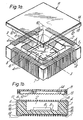
- a chip carrier 1 is moulded with a central die mounting cavity 2.
- a plurality of metallised contacts 4 are provided.
- Each of the contacts comprises a metallisation which extends from the carrier's upper surface, down the side wall, and onto the carrier's upper surface is coated with gold to form a pad suitable for wire bonding.
- the corresponding contact part 7 on the lower surface is coated with a metal such as tin or an alloy such as tin/lead suitable for forming a solderable contact pad.
- a die bonding pad 8 is formed by metallisation.
- a die 9 is shown bonded (for example, with an epoxy resin) to the die bonding pad. Electrical contact is made to the various parts of the die by bonding aluminium or gold wires 10 to the die 9 and to the wire bonding pads 6.
- a chip carrier as described above can be fabricated by injection moulding techniques.
- Suitable plastics for use in moulding such a chip carrier include aromatic polymers such as polyether ether ketone (PEEK) and polyethersulphone (PES) sold under the name VICTREX by ICI; polysulphone sold under the name UDEL by Union Carbine; and polyetherimide sold under the name ULTEM by General Electric.
- polyether ketone [-C6H4-CO-C6H4-O-C6H4-O-]n
- Polyethersulphone [-C6H4-SO2-C6H4-O-]n
- UDEL Polysulphone [-C6H4-SO2-C6H4-O-C6H4-C3H6-C6H4-O]n Polyetherimide - see Figure 7.
- a lid 11 is provided.
- the lid 11 is moulded from a material compatible with that of the body of the chip carrier to enable them to be joined without the use of glues, eg by ultrasonic welding.
- glues eg by ultrasonic welding.
- the contacts 4 are deposited on the surface of the chip carrier, they provide a stepped surface, and it is to this that the lid has to be sealed.
- the lid's lower surface is provided with indentations 12 in positions corresponding to the positions of contacts 4.
- the indentations are made somewhat smaller than the contacts 4 which they are to receive, and in the example shown they are triangular, with the apex uppermost.
- the lid may be made in two parts: the first part 13 comprises a sidewall, and the second part 14 a cap.
- the sidewall 13 is welded to the carrier body, encapsulant can then be applied to the wire bonded chip, and the cap 14 is then welded onto the sidewall 13.
- the contacts 4 comprise multiple metallic coatings; a first coating 15 of copper, a .25mm nickel coating 16 over the copper, a gold coating 17 over the nickel on the upper end of the contact to form the wire bonding pad 6, and a tin or tin/lead alloy coating 18 over the nickel of the lower end of the contact to form a solderable terminal pad 7.
- the die bonding pad 8 can advantageously have a construction whereby differential thermal expansion between the chip carrier and the die 9 itself is better accommodated.
- the carrier material has a typical TCE of 23x10 ⁇ 6 o C ⁇ 1, that of silicon is about 2x10 ⁇ 6 o C ⁇ 1.
- This construction could be such that the die bonding pad 8 comprises a relief pattern 30 such as series of ribs, concentric rings, or a plurality of "pillars", or be "maze” shaped (the latter two constructions being even more advantageous than the first because they admit differential expansion in all directions in the relevant plane).
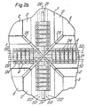
- the chip carriers made by injection moulding in thermoplastic may conveniently be moulded in a matrix of for example 10x10. Such a matrix is shown in Figure 2a, and details of the arrangement of conductors etc between adjacent carriers is shown in Figure 2b.
- the matrix is moulded as a generally flat sheet containing the die cavities and the necessary holes for producing conductors 4. Note that chip carriers may be moulded without cavities, deeper lids being provided to supply the die mounting cavity. Preferably, however, the carrier body will have a moulded-in die mounting cavity, as this offers a number of advantages, including some protection against accidental damage during processing.
- the described embodiments of the invention contemplate two alternative methods of producing the conductors 4 and die bonding pads 8.
- a copper coating is formed by lamination or electroless deposition and etched using conventional resist techniques: desired coatings of nickel, gold, tin, etc can then be selectively plated.
- all metallisation is initially carried out by electroless deposition and etching is unnecessary.
- the pattern, once defined, can be built up either electrolessly or by electroplating.
- Both methods have the advantage, as compared with processes where the final finish is used as a mask for etching the copper beneath, of avoiding the deposition of gold in areas where it is undesirable (for the reasons discussed earlier). This approach is made practicable by injection moulding whereby holes can be formed, easily at the moulding stage, avoiding a prohibitive amount of drilling being required to produce the necessary through-hole connections.
- the conductors 4 and die bonding pads 8 are produced after the matrix is moulded, and, for this reason, it is not necessary to provide any metallic inserts during moulding. Processing may be facilitated by producing plating bars 21 in rows or as a grid between the individual chip carriers. In this way it is possible, if desired, to connect together all the chip carriers to form a single electrode.
- the first stage in defining the conductor pattern involves rendering the surface of the plastic sufficiently sensitive to accept an electroless copper deposition.
- This may be done in any convenient way, although the preferred method is to use the resistless imaging process devised by PCK Technology of Melville New York and known as Photoforming.
- the moulding is chemically etched to render this surface hydrophilic to enable deposition of a catalyst and electroless copper.
- the surface is activated with a solution containing an ultra violet (UV) photo initiator and copper salts.
- UV light ultra violet
- electroless copper deposition can be used to produce a thicker copper layer which can be used as an electrode in subsequent electroplating steps. It should be noted that for use in such processes the polymers discussed require treatment, such as doping with titanium dioxide to render them opaque to ultra-violet light.
- plating bars ie broad tracks
- electroless copper plating step it may be possible to dispense with the electroless copper plating step, and simply electroplate on the pattern defined in the photoforming step.
- the die bonding pads may be formed by insertion of a metallic stud or in some other way which does not require the pads to be plated, in which case they need not form part of the electrode.
- the tracks 21 serve to interconnect these regions on all the carriers and are removed when the matrix is separated to form individual carriers. This is most easily done by arranging the tracks 21 in the form of a lattice with one chip carrier per cell.
- tracks 23 there are no contacts 4 at the corners of the chip carriers (as this could result in different path lengths between the die and the different terminal pads 7), and these spaces allow tracks 23 to be run from the die bonding pads to the tracks 21 of the lattice. Alternatively tracks could be run directly from a contact 4 at the centre of one side of the carrier to the die bonding pad. These could be cut at a later stage or (if external connection to the semiconductor substrate is required) allowed to remain.
- a hole or slot 24 is provided through the board.
- a metallised pad (which on the upper surface of the chip carrier will form wire bonding pads 6 or on the lower side of the chip carrier will form the terminal pads 7) is provided.
- the photoforming step provides sufficient metallic copper on the walls of the holes 24 for subsequent metallisation to give fully plated through holes.
- the wire bonding pads are plated with 2 micrometres of gold.
- taped resists ie resists or masks in the form of adhesive tapes
- the terminal pads may be pre-coated with a tin or lead alloy.
- the matrix of chip carriers can be divided into individual carriers either before or after dies are bonded and wired to the carriers, although usually the chip carriers will be separated before dies are bonded to them.
- the matrix of chip carriers can have lines of weakness moulded into it, along the edges of the plating bars for example, so that it is possible (depending upon the material used) to snap off lines of carriers or individual carriers. If the precursors of the contacts 4 are slots or a combination of slots and holes, it may be possible to use them so the line of weakness along which the chip carriers may be separated by 'snapping' apart. Alternatively, the matrix may be divided up using a saw, for example a circular saw. In either case the conductive tracks which have been used during electroplating are removed during separation of adjacent carriers.
- each of the boundaries of each chip carrier is defined by a separate row of holes, as in Figure 2b, so that between any two adjacent carriers there are two rows of holes
- the material removed during separation comprises that between the two rows of holes - viz by severing along lines 22 leaving each separated chip carrier with edges comprising flat portions between concave conductors 4.
- separation is along lines 52 leaving the holes 24 into which leads can be inserted.
- a further advantage of making chip carriers by injection moulding is that the material used can have a coefficient of thermal expansion similar to that of most of the metal cored printed circuit boards (PCB) and substrates.
- PCB printed circuit boards
- whole PCBs could be moulded having recesses at the chip sites like a multiple-chip carrier - and metallized as previously described.
- the chip would then be bonded into the cavities and protected with junction coatings.
- lids of the same nature as those proposed for the single-chip carrier could be welded into place to afford mechanical protection.
- the added benefit of this solution is that the tracking on the PCB could be taken directly into the chip housing and thus the problems of the package/board interface are removed.
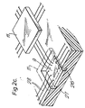
- Figure 2c is a perspective view of part of such a construction in which a chip 9 is accommodated in a rectangular recess 26 in an injection moulded substrate 27, a lid 11 is shown covering another recess.
- Another advantage of this arrangement is that the absence of a separate carrier between the chip and a PCB, coupled with the location of the chip in a recess means that the upper, connecting, surface of the chip can be arranged to be co-planar with conductive tracks 28 on the substrate, providing superior transmission - line properties for highspeed/high frequency operation.
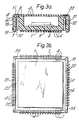
- FIG. 3 shows a chip carrier in which the side walls 31, which are metallised to form the contacts 4, are each separated from the main chip carrier body by a slot 32, which extends to virtually the full height of the side wall; this side wall being connected to the main body by only a thin elastically deformable portion 33.
- the provision of these deformable portions enables the chip carrier to repeatedly accommodate relatively large strains resulting from differential thermal expansion without imposing large stresses on the solder joints between the terminal pads and the circuit board.
- thermal path maybe incorporated in the die bond pad, and various arrangements are shown in Figures 4 and 5.
- the chip carrier shown in Figure 4 has several plated through holes 40 in the die bonding pad 8. These holes are produced at the same time and in the same way as the interconnection holes used to form the contacts 4. Alternatively, the holes can be left unplated and slugs of a thermally conductive material (eg copper) inserted. In either case, a thermal pad 41 on the underside of the chip carrier, corresponding to the die bond pad 8, would enhance heat transfer. For efficient heat transfer the thermal pad may be soldered to a corresponding contact on the circuit board to which the chip carrier is to be attached. Indeed, this form of attachment could be used as a means of mechanical anchorage even in the absence of thermally conductive material extending through the carrier.
- a thermally conductive material eg copper
- This solder connection can be replaced with a high heat conductivity grease to bridge any gap between the thermal pad and the circuit board.
- the thermal pad may not be connected to the circuit board but left to radiate heat, as for instance, when included in an injection moulded multiple chip carrier.
- a legged platform or stud 42 ( Figure 5) which can either be incorporated into the matrix during injection moulding, or inserted into a suitable hole formed during moulding.
- this stud may consist of two parts, an upper and a lower, which can be inserted or moulded in separately.
- the surface which is to be soldered comprises a number of discrete areas so that the formation of voids is minimised.
- the gauge length over which the thermal stress acts is considerably reduced. Without the central attachment provided by the thermal pad the gauge length would be the distance between the side walls. With a thermal pad this is reduced to just twice the distance between the thermal pad and the side wall, ie the gauge length is reduced by the width of the thermal pad.
- the problems of soldering the thermal pad 41 or an anchorage pad to a circuit board increase as the size of the chip (and carrier) increases.
- Reflow soldering is carried out by pre-coating the pad and contact pads with a solder paste comprising powdered solder, powdered flux and an organic binder.
- the application of heat (as uniformly as possible) by any of a number of known techniques, eg vapour phase soldering, causes flow of the solder and flux and a solder joint is formed.
- the proposed construction further allows the use of a small circuit board track width and separation which may enable greater circuit densities to be realised.
- This can be achieved by offsetting adjacent terminal contacts on the carrier, for example by providing an inner and an outer row of terminal contacts as shown in Figures 6. It can be seen that the edge of the chip carrier is castellated, with an inner and an outer row of contacts 4a, 4b; the size and offset being such that the inner terminal contacts can be inspected by looking through the gaps between adjacent outer terminal contacts. In this way, it is possible for all the contacts between a chip carrier and a circuit board to be visually inspected.
- the provision of an inner and an outer row of terminal contacts allows the pitch of the contacts to be reduced, and hence allows denser packing, while maintaining adjacent solder pad separation.
- the chip carriers may also be made compatible with circuit boards using plated through hole (pth) technology by providing them with leads.
- Such chip carriers are made as has been described above (although there is no need to provide terminal contacts on the carrier's lower surface), with each chip carrier having its own array of holes 24 which are to be used to provide contacts 4.
- the leads are inserted into the holes 24, either singly or in a ganged operation into several holes simultaneously using for example an automatic leading machine.
- the leads should be suitably sized to provide an efficient seal to the holes through which they pass.
- the connecting pieces between ganged leads can be removed, and the leads left straight for through board insertion of 'joggled' to form a surface mounting footprint.
Landscapes
- Structures Or Materials For Encapsulating Or Coating Semiconductor Devices Or Solid State Devices (AREA)
- Cooling Or The Like Of Semiconductors Or Solid State Devices (AREA)
Priority Applications (1)
| Application Number | Priority Date | Filing Date | Title |
|---|---|---|---|
| EP89109817A EP0334397A3 (de) | 1984-05-18 | 1985-05-16 | Schaltungsplatte |
Applications Claiming Priority (3)
| Application Number | Priority Date | Filing Date | Title |
|---|---|---|---|
| GB848412674A GB8412674D0 (en) | 1984-05-18 | 1984-05-18 | Integrated circuit chip carrier |
| GB8412674 | 1984-05-18 | ||
| EP89109817A EP0334397A3 (de) | 1984-05-18 | 1985-05-16 | Schaltungsplatte |
Related Parent Applications (2)
| Application Number | Title | Priority Date | Filing Date |
|---|---|---|---|
| EP85303447.8 Division | 1985-05-16 | ||
| EP85303447A Division EP0165705A1 (de) | 1984-05-18 | 1985-05-16 | Träger für integrierten Schaltungschip |
Publications (2)
| Publication Number | Publication Date |
|---|---|
| EP0334397A2 true EP0334397A2 (de) | 1989-09-27 |
| EP0334397A3 EP0334397A3 (de) | 1990-04-11 |
Family
ID=26120238
Family Applications (1)
| Application Number | Title | Priority Date | Filing Date |
|---|---|---|---|
| EP89109817A Withdrawn EP0334397A3 (de) | 1984-05-18 | 1985-05-16 | Schaltungsplatte |
Country Status (1)
| Country | Link |
|---|---|
| EP (1) | EP0334397A3 (de) |
Cited By (3)
| Publication number | Priority date | Publication date | Assignee | Title |
|---|---|---|---|---|
| WO1998015977A1 (en) * | 1996-10-10 | 1998-04-16 | Samsung Electronics Co., Ltd. | Hybrid high-power microwave-frequency integrated circuit |
| WO1998015980A1 (en) * | 1996-10-10 | 1998-04-16 | Samsung Electronics Co., Ltd. | Hybrid high-power integrated circuit |
| RU2489770C1 (ru) * | 2011-12-30 | 2013-08-10 | Федеральное государственное унитарное предприятие "Научно-производственное предприятие "Исток" (ФГУП НПП "Исток") | Гибридная интегральная схема свч |
Families Citing this family (1)
| Publication number | Priority date | Publication date | Assignee | Title |
|---|---|---|---|---|
| RU2161346C2 (ru) * | 1996-10-10 | 2000-12-27 | Самсунг Электроникс Ко., Лтд. | Мощная гибридная интегральная схема свч-диапазона |
Family Cites Families (3)
| Publication number | Priority date | Publication date | Assignee | Title |
|---|---|---|---|---|
| US3777220A (en) * | 1972-06-30 | 1973-12-04 | Ibm | Circuit panel and method of construction |
| JPS57196548A (en) * | 1981-05-28 | 1982-12-02 | Toshiba Corp | Plastic chip carrier |
| JPS57207356A (en) * | 1981-06-15 | 1982-12-20 | Fujitsu Ltd | Semiconductor device |
-
1985
- 1985-05-16 EP EP89109817A patent/EP0334397A3/de not_active Withdrawn
Cited By (3)
| Publication number | Priority date | Publication date | Assignee | Title |
|---|---|---|---|---|
| WO1998015977A1 (en) * | 1996-10-10 | 1998-04-16 | Samsung Electronics Co., Ltd. | Hybrid high-power microwave-frequency integrated circuit |
| WO1998015980A1 (en) * | 1996-10-10 | 1998-04-16 | Samsung Electronics Co., Ltd. | Hybrid high-power integrated circuit |
| RU2489770C1 (ru) * | 2011-12-30 | 2013-08-10 | Федеральное государственное унитарное предприятие "Научно-производственное предприятие "Исток" (ФГУП НПП "Исток") | Гибридная интегральная схема свч |
Also Published As
| Publication number | Publication date |
|---|---|
| EP0334397A3 (de) | 1990-04-11 |
Similar Documents
| Publication | Publication Date | Title |
|---|---|---|
| US4682270A (en) | Integrated circuit chip carrier | |
| US6020637A (en) | Ball grid array semiconductor package | |
| US5098864A (en) | Process for manufacturing a metal pin grid array package | |
| US5103292A (en) | Metal pin grid array package | |
| KR0184588B1 (ko) | 일체식 회로 패키지용 다층 리드프레임 | |
| US4750092A (en) | Interconnection package suitable for electronic devices and methods for producing same | |
| US5557150A (en) | Overmolded semiconductor package | |
| US5069626A (en) | Plated plastic castellated interconnect for electrical components | |
| US5710064A (en) | Method for manufacturing a semiconductor package | |
| US6395582B1 (en) | Methods for forming ground vias in semiconductor packages | |
| EP0352429B1 (de) | Automatische Bandmontage-Packung hoher Leistung vom Steckerstift-Typ | |
| EP0536418A1 (de) | Halbleiteranordnung und Verfahren zu dessen Herstellung | |
| US6323065B1 (en) | Methods for manufacturing ball grid array assembly semiconductor packages | |
| EP0771519A1 (de) | Packung elektronischer bauelemente mit integrierten kontaktlöchern | |
| HK1008113B (en) | Metal pin grid array package including dielectric polymer sealant | |
| WO1987004316A1 (en) | Ultra high density pad array chip carrier | |
| EP1171915B1 (de) | Elektrische leiteranordnung für ein halbleiterbauelement und verfahren zu ihrer herstellung | |
| TW518917B (en) | A tape carrier for semiconductor and the manufacturing method for the semiconductor and this tape carrier | |
| EP0333237A2 (de) | Integrierter Schaltungschipträger | |
| US20020003308A1 (en) | Semiconductor chip package and method for fabricating the same | |
| WO1989000346A1 (en) | Plated plastic castellated interconnect for electrical components | |
| EP0334397A2 (de) | Schaltungsplatte | |
| KR100359174B1 (ko) | 필름캐리어및이필름캐리어를이용한반도체장치 | |
| EP0117211A2 (de) | Verfahren zur Herstellung eines Gehäuses für integrierte Schaltungen | |
| CN115346967B (zh) | 三维堆叠屏蔽结构和三维堆叠屏蔽方法 |
Legal Events
| Date | Code | Title | Description |
|---|---|---|---|
| PUAI | Public reference made under article 153(3) epc to a published international application that has entered the european phase |
Free format text: ORIGINAL CODE: 0009012 |
|
| AC | Divisional application: reference to earlier application |
Ref document number: 165705 Country of ref document: EP |
|
| AK | Designated contracting states |
Kind code of ref document: A2 Designated state(s): AT BE CH DE FR GB IT LI LU NL SE |
|
| PUAL | Search report despatched |
Free format text: ORIGINAL CODE: 0009013 |
|
| AK | Designated contracting states |
Kind code of ref document: A3 Designated state(s): AT BE CH DE FR GB IT LI LU NL SE |
|
| STAA | Information on the status of an ep patent application or granted ep patent |
Free format text: STATUS: THE APPLICATION IS DEEMED TO BE WITHDRAWN |
|
| 18D | Application deemed to be withdrawn |
Effective date: 19901201 |