EP0335169A1 - Dispositif de commutation symétrique sans porte et de faible puissance reactive appliqué aux éléments de commutation semi-conducteurs d'un onduleur - Google Patents
Dispositif de commutation symétrique sans porte et de faible puissance reactive appliqué aux éléments de commutation semi-conducteurs d'un onduleur Download PDFInfo
- Publication number
- EP0335169A1 EP0335169A1 EP89104579A EP89104579A EP0335169A1 EP 0335169 A1 EP0335169 A1 EP 0335169A1 EP 89104579 A EP89104579 A EP 89104579A EP 89104579 A EP89104579 A EP 89104579A EP 0335169 A1 EP0335169 A1 EP 0335169A1
- Authority
- EP
- European Patent Office
- Prior art keywords
- switch
- relief
- inverter
- capacitor
- diode
- Prior art date
- Legal status (The legal status is an assumption and is not a legal conclusion. Google has not performed a legal analysis and makes no representation as to the accuracy of the status listed.)
- Withdrawn
Links
- 239000004065 semiconductor Substances 0.000 title claims abstract description 37
- 239000003990 capacitor Substances 0.000 claims abstract description 70
- 102100027557 Calcipressin-1 Human genes 0.000 abstract description 12
- 101100247605 Homo sapiens RCAN1 gene Proteins 0.000 abstract description 12
- 101150064416 csp1 gene Proteins 0.000 abstract description 12
- 101100441251 Arabidopsis thaliana CSP2 gene Proteins 0.000 abstract description 9
- 238000000034 method Methods 0.000 abstract description 5
- 229920006395 saturated elastomer Polymers 0.000 abstract 1
- 230000000694 effects Effects 0.000 description 3
- 230000007423 decrease Effects 0.000 description 2
- 230000005415 magnetization Effects 0.000 description 2
- 230000001172 regenerating effect Effects 0.000 description 2
- 230000004913 activation Effects 0.000 description 1
- 230000001419 dependent effect Effects 0.000 description 1
- 238000011161 development Methods 0.000 description 1
- 230000018109 developmental process Effects 0.000 description 1
- 238000011084 recovery Methods 0.000 description 1
- 230000036962 time dependent Effects 0.000 description 1
Images


Classifications
-
- H—ELECTRICITY
- H02—GENERATION; CONVERSION OR DISTRIBUTION OF ELECTRIC POWER
- H02M—APPARATUS FOR CONVERSION BETWEEN AC AND AC, BETWEEN AC AND DC, OR BETWEEN DC AND DC, AND FOR USE WITH MAINS OR SIMILAR POWER SUPPLY SYSTEMS; CONVERSION OF DC OR AC INPUT POWER INTO SURGE OUTPUT POWER; CONTROL OR REGULATION THEREOF
- H02M7/00—Conversion of AC power input into DC power output; Conversion of DC power input into AC power output
- H02M7/42—Conversion of DC power input into AC power output without possibility of reversal
- H02M7/44—Conversion of DC power input into AC power output without possibility of reversal by static converters
- H02M7/48—Conversion of DC power input into AC power output without possibility of reversal by static converters using discharge tubes with control electrode or semiconductor devices with control electrode
- H02M7/505—Conversion of DC power input into AC power output without possibility of reversal by static converters using discharge tubes with control electrode or semiconductor devices with control electrode using devices of a thyratron or thyristor type requiring extinguishing means
- H02M7/515—Conversion of DC power input into AC power output without possibility of reversal by static converters using discharge tubes with control electrode or semiconductor devices with control electrode using devices of a thyratron or thyristor type requiring extinguishing means using semiconductor devices only
- H02M7/5152—Conversion of DC power input into AC power output without possibility of reversal by static converters using discharge tubes with control electrode or semiconductor devices with control electrode using devices of a thyratron or thyristor type requiring extinguishing means using semiconductor devices only with separate extinguishing means
Definitions
- the invention relates to a device for low-loss relief when switching the semiconductor switches on and off in a single-phase or multi-phase inverter fed by a direct voltage source.
- Such a circuit is known, for example, from DE-OS 32 44 623 and is described in particular on page 131 in the "Elektrotechnische Zeitschrift (etz), Vol. 104, 1983, Issue 7/8, pages 328 to 332".
- This known wiring network is shown in FIG. 1 and consists of two cut-in relief chokes L1, L2, a cut-off relief capacitor C A , a storage capacitor C SP , two cut-off relief diodes D10, D20 and a discharge resistor R.
- the inverter phase shown which consists of antiparallel freewheeling diodes D1 , D2 connected semiconductor switches T1, T2 is connected to the positive or negative potential of the supplying DC voltage source u D at the upper or lower end B or C via a first or second switch-on relief choke L1 or L2 which acts as a current rise limitation.
- the shutdown relief capacitor C A is connected at one end to the load output A of the inverter phase.
- the series circuit comprising the storage capacitor C SP and the first shutdown relief diode D10 is arranged between the upper end B of the inverter phase and the other end of the shutdown relief capacitor C A.
- the second shutdown relief diode D20 finally connects the other end of the shutdown relief capacitor C A to the lower end C of the inverter phase.
- a discharge resistor R which is the connection point, serves to reduce the circuit energies temporarily stored in the switch-off relief and storage capacitor during a switch-off process connects between the storage capacitor and the first switch-off relief diode with the negative potential of the DC voltage source u D.
- a feedback device for example a so-called "chopper circuit" can be used, with the aid of which the wiring energies are fed back into the supplying direct voltage source u D.
- this wiring network has the disadvantage that it has an asymmetry caused by the circuitry.
- the series circuit comprising the storage capacitor C SP and the switch-off relief capacitor C A has a relief.
- the lower semiconductor switch T2 is switched off, only the switch-off relief capacitor C A has a relief.
- Such an asymmetry has the consequence that the semiconductor switches T1, T2, which are generally identical, are not relieved in the same way. In particular when designing such a circuit, it must therefore be taken into account that when the semiconductor switches T1 and T2 are switched off, different rates of rise occur in the recurring positive reverse voltage at the respective switch.
- the circuit has the further disadvantage that, due to the discharge resistance, pulse-like currents occur in the feed lines to the supply source.
- the temporarily stored energies are returned to the source u D.
- this corresponds to a "commutation reactive power" required by the inverter, which must be provided periodically by the supplying DC voltage source for the purpose of relieving the inverter semiconductor switches off and on.
- it is not always possible and permissible to apply such pulsating recharging energies to the input DC voltage source.
- the invention is based on the object of specifying a wiring network which, as far as possible without stress on the supplying DC voltage source, enables low-loss and symmetrical switch-off and switch-off relief of the semiconductor switches of an inverter.
- FIG. 2 shows the device according to the invention for low-loss relief when the semiconductor switches of an inverter are switched on and off.
- a phase of an inverter is shown as the power part LT, the upper or lower part of which consists of the semiconductor switch T1 with the antiparallel freewheeling diode D1 or the semiconductor switch T2 and the freewheeling diode D2.
- the output of this phase is designated A, the upper and lower connection with B and C.
- the present invention is such a power section, which generally consists of several phases, at its upper and lower ends B, C via a so-called "step inductor" L S1 or L S2 with a positive or negative potential which serves as a saturable inductance DC voltage source u D connected.
- each phase of the inverter is provided with a wiring network BN for low-loss and low reactive power switching relief of the semiconductor switching elements T1, T2 during the switching on and off process.
- a first and second storage capacitor C SP1 , C SP2 and a cut-off relief capacitor C A have a switch-off- relief effect
- a first and a second cut-in relief choke L1, L2 have a cut-off relief effect.
- the cut-off relief capacitor C A is connected to the output A of the power section at one connection in accordance with FIG.
- a first or second series circuit comprising the first storage capacitor C SP1 and a first shutdown relief diode D10 or the second storage capacitor C SP2 and a second shutdown relief diode D20 further connect the upper end B of the power section LT to the other terminal of the shutdown relief capacitor C A , or the latter with the lower end C of the power section.
- the connection point between the first storage capacitor C SP1 and the first switch-off relief diode D10 in the first series connection is furthermore via the second switch-on relief choke L2 and a third or fourth regenerative diode D22 or D21 with the lower end C of the power section or the negative potential of the DC voltage source u D in connection.
- connection point between the second storage capacitor C SP2 and the second cut-off relief diode D20 is in the second series connection via the first cut-in relief choke L1 and a first or second regenerative diode D12 or D11 with the upper end B of the power section LT or the positive potential of the DC voltage source u D in connection.
- the device according to the invention has the particular advantage that there is no internal asymmetry in the circuit. Rather, when the upper or lower semiconductor switch T1 or T2 is switched off, the series arrangement comprising the first storage capacitor C SP1 and the switch-off relief capacitor C A or the series arrangement comprising the second storage capacitor C SP2 and the switch-off relief capacitor C A has a switch-off relief. Since the relationship is advantageous for the capacitance values of the capacitors C SP1 ⁇ C SP2 »C A applies, the recurring positive reverse voltages at the upper and lower semiconductor switches T1, T2 have approximately the same rise rates.
- the step chokes L S1 , L S2 according to the invention between the upper and lower ends B, C of the power section LT and the positive or negative potential of the DC voltage source act approximately like "time-dependent switches". If a voltage is applied to such an inductor in the demagnetized state, its internal “step core” must first be magnetized until the saturation state occurs. In the so-called “step time” caused thereby, the step inductor has an almost infinitely large inductance and allows only a very small current flow. On the other hand, after this step time has elapsed, ie after the saturation state of the step core has been reached, the inductor loses its inductance almost completely.
- the step choke is now quasi “switched on” and a current flow in the full amount caused by the other circuit parts is possible.
- this property of the step inductors L S1 and L S2 is used, in particular when a semiconductor switch is switched on, to temporarily decouple the wiring network BN from the direct voltage source u D.
- the overcharge contained in the storage capacitors C SP1 , C SP2 due to a previous shutdown of the valves and the magnetization contained in the switch-on relief chokes L1, L2 due to the activation in the load located at output A of the power section LT of the inverter phase feed.
- the DC voltage source u D is therefore no longer loaded with pulsed charge-reversal currents. Since consequently the DC voltage source in particular does not itself have to resume the circuit energies temporarily stored in the circuit network, it does not have to provide any "commutation reactive power" to maintain the functionality of the switching relief device according to the invention. Rather, the portion of the energy of the DC voltage source that has to be buffered during a switching cycle from a semiconductor switch-off and switch-on for the purpose of switching relief in the wiring network BN is passed on to the load to be fed almost without loss at the end of the cycle.
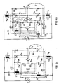
- FIGS. 3a to 3d show, by way of example, the “current paths” which arise when the semiconductor switch T1 is switched off
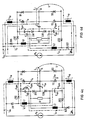
- FIGS. 4a to 4d show the “current paths” which result when the same semiconductor switch T1 is switched on again.
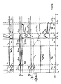
- these “current paths” in particular are explained in more detail with reference to the current and voltage profiles shown in FIG.
- the time axis in FIG. 5 shows which section of the current and voltage profiles can be assigned to the circuit states shown in FIGS. 3a to 3d and 4a to 4d.
- FIG. 3a the steady state of the circuit of FIG. 2 is shown in FIG. 3a, in which, when the upper semiconductor switch T1 is switched on, the load current i L in full via the first step inductor L S1 and the phase output A into the load L, and from there via the second step inductor L S2 flows back into the circuit.
- the supply current i ZUL in the lines connecting the direct voltage source u D is equal to the load current i L.
- the wiring network itself is currentless in this initial state, and the storage capacitors C SP1 , C SP2 and the switch-off capacitor C A are charged to half the value of the direct voltage u D / 2 with the directions shown in FIG. 3a. 5 shows the associated current and voltage profiles between the times t0 and t1.
- the load current i L commutates immediately to the wiring network.
- a current path is formed via the first storage capacitor C SP1 , the first switch-off relief diode D10 and the switch-off relief capacitor C A to the phase output A.
- the switch-off relief capacitor C A is again charged approximately in the direction of the capacitor voltage u CA shown in FIG. 3b to half the value of the direct voltage u D.
- the second cut-off relief diode D20 becomes conductive. This is in FIG 3c and in FIG 5 between the times t2 and t3 shown.
- the current i CSP1 flowing through the first series circuit from the first storage capacitor and the first shutdown discharge diode is now divided into a portion i CA flowing through the shutdown discharge capacitor C A and the load L, and into a portion i CA flowing through the second series circuit from the second shutdown discharge diode D20 and portion i CSP2 flowing to the second storage capacitor C SP2 .
- the load current i L increasingly commutates to the freewheeling diode D2.
- the supply current i ZUL comes to a standstill.
- the load current i L flows in full freewheeling as diode current i D2 via the freewheeling diode D2. This state is shown in FIG 3d and 5 in the area between t3 and t4. It can be seen that all equalizing currents in the wiring network and in the step reactors have come to a standstill and that all capacitors are slightly overloaded.
- step time of the step inductors begins to "run out” in that the supply current i ZUL, which is only gradually increasing and for this reason not yet shown in FIG. 4a, magnetizes the step inductors L S1 , L S2 .
- the two resonant circuit currents i L1 and i L2 are forced to flow in the form of the current i T1 via the upper semiconductor switch T1.
- the current i D2 through the freewheeling diode decreases increasingly, and the load current i L is increasingly forced to flow through the upper semiconductor switch T1 again.
- FIG. 4b and the area between the times t5 and t6 in FIG. 5 show the state after which the current through the freewheeling diode D2 has come to a complete standstill. Since the inverter and the wiring network are still decoupled from the supplying DC voltage source via the step reactors L S1 , L S2 , the load current i L is fed exclusively by the resonant circuit currents i L1 and i L2 . The charge-reversal current i CA shown in dotted lines in FIG. 4b is superimposed on this. It is a particular advantage of the circuitry according to the invention that this charge reversal current is conducted via the semiconductor switching element T1 and thus does not burden the DC voltage source in any way.
- the charge-reversal current causes the cut-off relief capacitor C A to be recharged to that shown in FIG. 4b Voltage direction U CA.
- This reloading is required so that the switch-off relief capacitor can have a switch-off relief when the semiconductor switch T1 is switched off again.
- the originally existing overload of the switch-off relief capacitor is dissipated into the load in a particularly advantageous manner as part of the load current i L.
- the swinging process is ended when the capacitor voltage u CA has reached the value of the voltage u CSP1 at the first storage capacitor C SP1 .
- This current also temporarily contributes to the supply of the load current i L , so that the circuit energies buffered in the chokes L 1, L 2 are almost completely made available to the load.
- the Zu only reaches after this discharge current has subsided line current i ZUL again the value of the load current i L. All compensation processes are completed and beyond the point in time t FIG in FIG. 5 there is the initial state shown in FIG. 3a.
- the switching relief device works almost loss-free with a load current i L assumed to be constant.
- the wiring energies temporarily stored in the wiring network BN and the step inductors L S1 , L S2 can be almost completely fed into the load, in particular if the step time of the step inductors is greater than that for reloading the cut-off relief capacitor during a switching operation, in particular one Switching on one of the semiconductor switches takes time, and the step reactors have almost ideal "switching behavior".
- the load current i L will often not be ideally constant in particular if the load acts on the phase output A with its own countervoltage. If, for example, an electrical machine serves as a load, the induced voltage which is dependent on the angular velocity acts as such a counter-voltage. In such a case, the load current is subject to a harmonic whose frequency is essentially determined by the speed at which the semiconductor switches in the inverter switch on and off. Due to the changing instantaneous value of the load current, the wiring energies cannot therefore be completely fed into the load via the slightly asymmetrical resonant circuit currents i L1 , i L2, in particular in the state of the circuit shown in FIG. 4c.
Landscapes
- Engineering & Computer Science (AREA)
- Power Engineering (AREA)
- Inverter Devices (AREA)
Applications Claiming Priority (2)
| Application Number | Priority Date | Filing Date | Title |
|---|---|---|---|
| DE3810535 | 1988-03-28 | ||
| DE3810535 | 1988-03-28 |
Publications (1)
| Publication Number | Publication Date |
|---|---|
| EP0335169A1 true EP0335169A1 (fr) | 1989-10-04 |
Family
ID=6350906
Family Applications (1)
| Application Number | Title | Priority Date | Filing Date |
|---|---|---|---|
| EP89104579A Withdrawn EP0335169A1 (fr) | 1988-03-28 | 1989-03-15 | Dispositif de commutation symétrique sans porte et de faible puissance reactive appliqué aux éléments de commutation semi-conducteurs d'un onduleur |
Country Status (3)
| Country | Link |
|---|---|
| US (1) | US4924370A (fr) |
| EP (1) | EP0335169A1 (fr) |
| ZA (1) | ZA892203B (fr) |
Cited By (3)
| Publication number | Priority date | Publication date | Assignee | Title |
|---|---|---|---|---|
| DE4121177A1 (de) * | 1990-06-23 | 1992-01-16 | Licentia Gmbh | Schaltungsanordnung zur abschaltentlastung eines wechselrichterzweigpaares |
| DE4042378A1 (de) * | 1990-06-23 | 1992-01-16 | Licentia Gmbh | Symmetrische schaltentlastungsanordnung fuer ein aus gategesteuerten halbleiterschaltern gebildetes wechselrichterzweigpaar |
| EP0538851A3 (en) * | 1991-10-22 | 1993-08-04 | Hitachi, Ltd. | Power converter |
Families Citing this family (5)
| Publication number | Priority date | Publication date | Assignee | Title |
|---|---|---|---|---|
| DE59008372D1 (de) * | 1990-08-02 | 1995-03-09 | Asea Brown Boveri | Viertelbrückenschaltung für grosse Ströme. |
| DE59010931D1 (de) * | 1990-12-08 | 2003-03-06 | Abb Schweiz Ag | Schaltanordnung für einen HF-GTO |
| US5450308A (en) * | 1994-02-23 | 1995-09-12 | Kabushiki Kaisha Toshiba | Gate power supply circuit |
| AU2003272229A1 (en) * | 2002-08-19 | 2004-03-03 | Don W. Phillips | Ratchet with substantially silent movement-prevention mechanism |
| DE102016215657A1 (de) * | 2016-08-19 | 2018-02-22 | Lenze Automation Gmbh | Verfahren zum Erzeugen eines digitalen Signals aus einem analogen Signal und Frequenzumrichter |
Citations (2)
| Publication number | Priority date | Publication date | Assignee | Title |
|---|---|---|---|---|
| DE3244623A1 (de) * | 1982-04-27 | 1984-09-27 | Rainer Dr Ing Marquardt | Beschaltung fuer elektronische zweigpaare in antiparallelschaltung |
| DE3524522A1 (de) * | 1985-07-05 | 1987-01-15 | Matthias Jung | Rueckspeisende beschaltung fuer elektronische zweigpaare in antiparallelschaltung |
Family Cites Families (3)
| Publication number | Priority date | Publication date | Assignee | Title |
|---|---|---|---|---|
| DE149140C (fr) * | ||||
| US4611267A (en) * | 1985-02-25 | 1986-09-09 | General Electric Company | Snubber arrangements with energy recovery for power converters using self-extinguishing devices |
| US4691270A (en) * | 1986-07-22 | 1987-09-01 | Rca Corporation | Current fed inverter bridge with lossless snubbers |
-
1989
- 1989-03-15 EP EP89104579A patent/EP0335169A1/fr not_active Withdrawn
- 1989-03-21 US US07/326,608 patent/US4924370A/en not_active Expired - Fee Related
- 1989-03-23 ZA ZA892203A patent/ZA892203B/xx unknown
Patent Citations (2)
| Publication number | Priority date | Publication date | Assignee | Title |
|---|---|---|---|---|
| DE3244623A1 (de) * | 1982-04-27 | 1984-09-27 | Rainer Dr Ing Marquardt | Beschaltung fuer elektronische zweigpaare in antiparallelschaltung |
| DE3524522A1 (de) * | 1985-07-05 | 1987-01-15 | Matthias Jung | Rueckspeisende beschaltung fuer elektronische zweigpaare in antiparallelschaltung |
Non-Patent Citations (1)
| Title |
|---|
| ELEKTROTECHNISCHE ZEITSCRIFT vol. 104, no. 7/8, 1983, Seite 328 - 332; K. HEUMANN et al: "GTO-Thyristoren in sebstgeführten Stromrichtern" * |
Cited By (4)
| Publication number | Priority date | Publication date | Assignee | Title |
|---|---|---|---|---|
| DE4121177A1 (de) * | 1990-06-23 | 1992-01-16 | Licentia Gmbh | Schaltungsanordnung zur abschaltentlastung eines wechselrichterzweigpaares |
| DE4042378A1 (de) * | 1990-06-23 | 1992-01-16 | Licentia Gmbh | Symmetrische schaltentlastungsanordnung fuer ein aus gategesteuerten halbleiterschaltern gebildetes wechselrichterzweigpaar |
| EP0538851A3 (en) * | 1991-10-22 | 1993-08-04 | Hitachi, Ltd. | Power converter |
| US5535114A (en) * | 1991-10-22 | 1996-07-09 | Hitachi, Ltd. | Power converter |
Also Published As
| Publication number | Publication date |
|---|---|
| US4924370A (en) | 1990-05-08 |
| ZA892203B (en) | 1989-11-29 |
Similar Documents
| Publication | Publication Date | Title |
|---|---|---|
| DE3743436C1 (de) | Schaltentlasteter,verlustarmer Dreipunktwechselrichter | |
| EP3278441B1 (fr) | Convertisseur multi-niveaux a pertes reduites | |
| DE2050783A1 (de) | Schaltung für ein Netzteil | |
| DE1763835A1 (de) | Wechselrichter | |
| EP1047180A2 (fr) | Convertisseur à trois-points ou à multi-points du type ARCP (Auxilliary Resonant Commutated Pole) | |
| EP2709257A2 (fr) | Circuit de convertisseur de courant et procédé de commande du circuit de convertisseur de courant | |
| EP0203571B1 (fr) | Onduleur statique avec surélévation de courant en cas de court-circuit | |
| DE3429488A1 (de) | Elektronische schaltvorrichtung | |
| EP3931953A1 (fr) | Procédé de limitation de courant en cas de variations transitoires de tension en une sortie de courant alternatif d'un onduleur à multiples étages et onduleur à multiples étages | |
| DE3743437C1 (en) | Low-loss, three-point invertor which is relieved of switching loads | |
| DE3714175C2 (fr) | ||
| WO2021160872A1 (fr) | Agencement de circuit pour équilibrer une liaison cc divisée | |
| DE4121177C2 (fr) | ||
| EP1358711B1 (fr) | Dispositif convertisseur de puissance pour un des divers bobinages d'un moteur a reluctance | |
| DE2739387A1 (de) | Schaltregler, insbesondere doppelpulsiger schaltregler | |
| EP1553686B1 (fr) | Alimentation de courant continu à haute tension et méthode d'opération de telle alimentation de courant continu à haute tension | |
| EP0539902B1 (fr) | Circuit électrique de dégagement au blocage pour un convertisseur de tension continu | |
| DE3833700C2 (fr) | ||
| AT399068B (de) | Schaltungsanordnung für einen zweipunkt-wechselrichterschaltpol | |
| AT527201B1 (de) | Hochsetzsteller mit gekoppelten Spulen und zwei Eingriffsmöglichkeiten | |
| DE102014110491A1 (de) | Schaltungsanordnung für einen mehrphasigen Mehrpunktwechselrichter mit Entlastungsnetzwerk | |
| DE4106045C1 (en) | Multi-phase semiconductor three-stage AC inverter - has low inductance capacitors which limit sheet duration voltage transients | |
| DE3436656C2 (fr) | ||
| DE3823399A1 (de) | Entlastungsnetzwerk fuer elektronische zweigpaare in antiparallelschaltung | |
| DE2012893C3 (de) | Schaltungsanordnung zur Zwangskommutierung eines Drehstrom-Wechselrichters |
Legal Events
| Date | Code | Title | Description |
|---|---|---|---|
| PUAI | Public reference made under article 153(3) epc to a published international application that has entered the european phase |
Free format text: ORIGINAL CODE: 0009012 |
|
| AK | Designated contracting states |
Kind code of ref document: A1 Designated state(s): AT BE CH DE FR GB IT LI SE |
|
| 17P | Request for examination filed |
Effective date: 19891026 |
|
| STAA | Information on the status of an ep patent application or granted ep patent |
Free format text: STATUS: THE APPLICATION HAS BEEN WITHDRAWN |
|
| 18W | Application withdrawn |
Withdrawal date: 19910308 |
|
| R18W | Application withdrawn (corrected) |
Effective date: 19910308 |