EP0336392A2 - Convertisseur auto-oscillant à sortie asymétrique et procédé de mise en oeuvre - Google Patents
Convertisseur auto-oscillant à sortie asymétrique et procédé de mise en oeuvre Download PDFInfo
- Publication number
- EP0336392A2 EP0336392A2 EP89105962A EP89105962A EP0336392A2 EP 0336392 A2 EP0336392 A2 EP 0336392A2 EP 89105962 A EP89105962 A EP 89105962A EP 89105962 A EP89105962 A EP 89105962A EP 0336392 A2 EP0336392 A2 EP 0336392A2
- Authority
- EP
- European Patent Office
- Prior art keywords
- switching element
- transformer
- capacitor
- current
- transistor
- Prior art date
- Legal status (The legal status is an assumption and is not a legal conclusion. Google has not performed a legal analysis and makes no representation as to the accuracy of the status listed.)
- Withdrawn
Links
- 238000000034 method Methods 0.000 title claims abstract description 16
- 238000004804 winding Methods 0.000 claims abstract description 65
- 239000003990 capacitor Substances 0.000 claims abstract description 56
- 230000007423 decrease Effects 0.000 claims abstract description 10
- 230000003247 decreasing effect Effects 0.000 claims description 3
- XEEYBQQBJWHFJM-UHFFFAOYSA-N Iron Chemical group [Fe] XEEYBQQBJWHFJM-UHFFFAOYSA-N 0.000 claims description 2
- 230000000903 blocking effect Effects 0.000 claims description 2
- 230000001105 regulatory effect Effects 0.000 abstract description 2
- 238000010586 diagram Methods 0.000 description 4
- 230000007704 transition Effects 0.000 description 3
- 230000033228 biological regulation Effects 0.000 description 2
- 229920006395 saturated elastomer Polymers 0.000 description 2
- 239000004065 semiconductor Substances 0.000 description 2
- XUIMIQQOPSSXEZ-UHFFFAOYSA-N Silicon Chemical compound [Si] XUIMIQQOPSSXEZ-UHFFFAOYSA-N 0.000 description 1
- 230000003321 amplification Effects 0.000 description 1
- 239000013078 crystal Substances 0.000 description 1
- 230000001419 dependent effect Effects 0.000 description 1
- 238000009795 derivation Methods 0.000 description 1
- 238000005265 energy consumption Methods 0.000 description 1
- 239000013642 negative control Substances 0.000 description 1
- 238000003199 nucleic acid amplification method Methods 0.000 description 1
- 239000013641 positive control Substances 0.000 description 1
- 238000000926 separation method Methods 0.000 description 1
- 229910052710 silicon Inorganic materials 0.000 description 1
- 239000010703 silicon Substances 0.000 description 1
- 230000001629 suppression Effects 0.000 description 1
Images


Classifications
-
- H—ELECTRICITY
- H02—GENERATION; CONVERSION OR DISTRIBUTION OF ELECTRIC POWER
- H02M—APPARATUS FOR CONVERSION BETWEEN AC AND AC, BETWEEN AC AND DC, OR BETWEEN DC AND DC, AND FOR USE WITH MAINS OR SIMILAR POWER SUPPLY SYSTEMS; CONVERSION OF DC OR AC INPUT POWER INTO SURGE OUTPUT POWER; CONTROL OR REGULATION THEREOF
- H02M3/00—Conversion of DC power input into DC power output
- H02M3/22—Conversion of DC power input into DC power output with intermediate conversion into AC
- H02M3/24—Conversion of DC power input into DC power output with intermediate conversion into AC by static converters
- H02M3/28—Conversion of DC power input into DC power output with intermediate conversion into AC by static converters using discharge tubes with control electrode or semiconductor devices with control electrode to produce the intermediate AC
- H02M3/325—Conversion of DC power input into DC power output with intermediate conversion into AC by static converters using discharge tubes with control electrode or semiconductor devices with control electrode to produce the intermediate AC using devices of a triode or a transistor type requiring continuous application of a control signal
- H02M3/335—Conversion of DC power input into DC power output with intermediate conversion into AC by static converters using discharge tubes with control electrode or semiconductor devices with control electrode to produce the intermediate AC using devices of a triode or a transistor type requiring continuous application of a control signal using semiconductor devices only
- H02M3/338—Conversion of DC power input into DC power output with intermediate conversion into AC by static converters using discharge tubes with control electrode or semiconductor devices with control electrode to produce the intermediate AC using devices of a triode or a transistor type requiring continuous application of a control signal using semiconductor devices only in a self-oscillating arrangement
- H02M3/3385—Conversion of DC power input into DC power output with intermediate conversion into AC by static converters using discharge tubes with control electrode or semiconductor devices with control electrode to produce the intermediate AC using devices of a triode or a transistor type requiring continuous application of a control signal using semiconductor devices only in a self-oscillating arrangement with automatic control of output voltage or current
Definitions
- the invention relates to a method for operating a self-oscillating single-ended converter, wherein by connecting the converter to the operating voltage, a capacitor connected in parallel with a switching element of the converter is charged via a primary winding of a voltage translation transformer of the converter, a control signal for a switching element is given by a control unit or control unit, and thereby Switching element is opened. Furthermore, depending on the value or timing of the current flowing through the switching element, the switching element is blocked by means of a control signal taken from the feedback winding of the transformer. Then the switching element is opened again at a predetermined value of the decreasing operating current flowing via the switching element. The opening and locking of the switching element is repeated periodically.
- the invention further relates to a self-oscillating single-ended converter, which contains a voltage-converting transformer, preferably a high-frequency transformer, a switching element connected to the primary winding of the transformer and connected in series with the primary winding, one end of the primary winding of the transformer and a terminal of the switching element optionally via a Current sensor stage are connected to the operating voltage terminals of the converter, and with a capacitor connected to a common terminal of the primary winding of the transformer and the switching element, the other connecting terminal of which is also connected to the operating voltage together with the terminal of the primary winding of the transformer or the switching element, furthermore with a from the feedback winding of the transformer, a capacitor and a resistor existing row element, which is connected to the control input of the switching element, also with a starting resistor connected to the operating voltage, which is also connected to a control input of the switching element.
- a voltage-converting transformer preferably a high-frequency transformer
- a switching element connected to the primary winding of the transformer and connected in series with
- the transformer producing the voltage required for the load generally a high-frequency transformer with an iron core, via its primary winding with a switching element, in principle with one High-performance switching transistor, is connected in series.
- the transistor is bridged by a capacitor, while its base is connected via a starting resistor to the operating voltage and to a series element composed of the feedback winding of the transformer, a capacitor and a resistor.
- the capacitor which also determines the operating frequency of the converter, is charged to the operating voltage value via the primary winding of the transformer.
- the control current flowing into the base of the switching transistor via the starting resistor begins to charge the base capacitor and when the voltage of this base capacitor exceeds the opening voltage of the switching transistor, the switching transistor also begins to open and reduces the voltage of the capacitor connected to its collector.
- the voltage occurring at the primary winding of the transformer is transformed in the same phase to the secondary winding or to the load. This voltage generates an additional base current via the feedback winding of the transformer, the base capacitor connected in series therewith and the resistor, and causes the switching transistor to open more.
- This self-amplifying process causes the switching transistor to saturate and switch the full operating voltage to the primary winding of the transformer.
- the collector current of the switching transistor increases exponentially during the load, while the base current of the switching transistor also decreases exponentially due to the charge of the capacitor of the LCR element. If the base current falls below a limit value that can be calculated using the ratio of the collector current and the cross-signal current amplification factor, the switching transistor becomes saturated and its collector voltage begins to grow at a speed determined by the connected capacitor. The voltage on the primary winding of the transformer decreases, as a result of which the voltage of the feedback winding of the transformer also decreases, which causes a further decrease in the base current of the switching transistor. At the end of the process, the switching transistor is blocked, a base current flows in the reverse direction, the collector voltage of the switching transistor describes a distorted half-waveform, then one third or half of the operating voltage is opened again and the process described is repeated periodically.
- the circuit described has numerous shortcomings that limit an advantageous application.
- the base of the switching transistor hangs in the air on the DC side, so the highly temperature-dependent internal current I CB0 with the control base current causes control problems .
- this current can also reach such a value that the system can no longer be regulated and dissipation in the switching transistor is too high.
- the voltage applied to the converter has a value of approximately 300 V.
- the collector voltage of the switching transistor should be increased to a voltage of 800-1000V in order to achieve high efficiency and good energy consumption.
- the circuit Since the usual transistor types can only withstand a fixed, defined maximum voltage without damage, the circuit is not reliable if the base-emitter junction of the transistor is not terminated with a low impedance.
- the switching transistor should be opened before its collector voltage drops to zero. If the switching transistor is opened again in the usual way at a one-third value of the operating voltage, the energy of the connected capacitor should then be dissipated by the switching transistor. According to practical experience, this means a loss of approximately 1 w. If the switching transistor is opened again close to the collector voltage of 200 V - and this happens quite often due to the stability and controllability - the specified loss increases fourfold, which is already significantly high for the semiconductor. In addition to the loss, the reliability of the circuit is also reduced to a great extent by the fact that the transistor is to withstand the shock-like stresses which cause local overloads in its crystal structure.
- the base current decreases in contrast to the increasing collector current, which also increases the losses of the switching transistor.
- the aim of the invention is to improve the operation of the known self-oscillating single-ended converters by means of a novel control and a newly developed circuit arrangement.
- the invention is based on the knowledge that the basic Emitter transition of the switching transistor should be emptied so that the regulation is made independent of the current I CBO of the switching transistor.
- the switching transistor may only be controlled in the open state when there is no voltage, and the base current of the switching transistor should have a corresponding reserve.
- the switching transistor should be blocked abruptly so that loss-increasing transients cannot occur.
- the control input of the switching element is terminated by means of low impedance and galvanically, and the switching element is switched on again in that time range, the beginning of which by the decrease in the voltage measured at the switching element to zero and the end by the decay of the current flowing through the switching element Current having polarity is determined, furthermore a control current proportional to the operating current flowing through the switching element or an almost constant control current is passed via the switched-on switching element, then the switching element is switched off independently of the instantaneous operating parameters of the converter at high speed.
- the rapid shutdown with low impedance of the switching transistor used as the switching element is carried out with the aid of an auxiliary switching element such that the base-emitter path of the switching transistor is emptied by opening the auxiliary switching element.
- the point in time at which the switching element is switched on is determined within the range of the predetermined time range so that the difference function of the voltage measured at the switching element is observed, and a control signal for switching on the switching element is output when the difference function suddenly drops to zero.
- a self-oscillating single-ended converter which contains a voltage-converting transformer, preferably a high-frequency transformer, a switching element connected to the primary winding of the transformer and connected in series with the primary winding, one end of the primary winding of the transformer and one terminal of the Switching elements, if necessary, are connected via a current sensor stage to the operating voltage terminals of the converter, and with a capacitor connected to a common terminal of the primary winding of the transformer and the switching element, the other terminal of which is also connected to the operating voltage together with the terminal of the primary winding of the transformer or the switching element , further comprising a series element consisting of the feedback winding of the transformer, a capacitor and a resistor, which is connected to the control input of the switching element is closed, also with a starting resistor connected to the operating voltage, which is also connected to a control input of the switching element.
- a voltage-converting transformer preferably a high-frequency transformer
- a switching element connected to the primary winding of the transformer and connected in series with the
- a control input of an auxiliary switching element is connected to a common terminal of the switching element and the current sensor stage, and the output connections of the auxiliary switching element are connected to the control input of the switching element, furthermore an input of a differential stage with the capacitor from which is connected to the feedback winding of the transformer feedback winding-capacitor resistor connected in series connected existing LCR element, the output of the differential stage being connected to a further control input of the auxiliary switching element.
- a switching transistor is used as the switching element of the converter, the collector gate of which is connected to one terminal of the primary winding of the transformer and to one terminal of a parallel capacitor-diode element, the other terminal of the primary winding being connected to the operating voltage and the other Terminal of the parallel element are connected to ground, and the emitter of the switching transistor is connected to ground via an emitter resistor used as a current sensor stage, and is also connected via a series resistor to the base of an npn small signal transistor forming the auxiliary switching element, a base resistor being connected to the base of the transistor mentioned so that the delay capacitor connected in parallel and also a decoupling diode of the differential stage are connected, and the base of the switching transistor is connected via the starting resistor to the positive operating voltage, to the collector of the auxiliary switching element Set transistor and connected to the resistor of the series element, while the differential stage is formed by the capacitor connected to the common terminal of the feedback winding and the capacitor connected in series therewith and by a parallel resistance
- control input of the converter is connected to the base of the transistor used as an auxiliary switching element via a signal level adjustment resistor.
- the emitter of the transistor forming the auxiliary switching element is connected to ground.
- the emitter of the transistor forming the switching element is connected to a potential which is more negative than the ground potential.
- the method according to the invention have the advantage that a simply constructed and reliable converter is created which enables the applications which have been avoided in practice for reasons of stability and reliability problems.
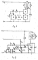
- FIG. 1 The block diagram shown in FIG. 1 is connected to terminals of a known DC power supply, not shown in the drawing.
- a primary winding L1 of a voltage-increasing high-frequency transformer TR is connected to the positive operating voltage + U t and a terminal of a switching element K, while a secondary winding L2 of the transformer RT is connected to a load element 7.
- Another terminal of the switching element K is connected to ground potential via a current sensor stage S.
- the switching element K and the current sensor stage S are bridged with a capacitor C.
- the output of the current sensor stage S is connected to a control input of an auxiliary switching element SK, one terminal of which is connected to ground and the other terminal of which is connected to the control input of the switching element K.
- the LCR element consists of a series-connected feedback winding L v of the transformer TR, a capacitor C b and a resistor R b .
- the feedback winding L v and the capacitor C b have a common terminal to which an input of a differential stage D is connected, the output of this differential stage D being connected to the second control input of the auxiliary switching element SLK.
- the switching element K is designed with a switching transistor T1 and the current sensor stage S is formed by a resistor R s .
- a diode D1 with opposite polarity to the switching transistor T1 is connected in parallel with the encoder C.
- the auxiliary switching element SK contains a further transistor T ⁇ , the emitter of which is connected to ground and the collector of which is connected to the base of the switching transistor T1 and the base to the common terminal of a parallel element connected to ground and a series resistor R e .
- the parallel element consists of a resistor R p and a capacitor C p .
- the other clamp of the Ballast resistor R e is connected to the emitter of switching transistor T1.
- the differential stage D contains a capacitor C d , which is connected with its one terminal to the feedback winding L v and its other terminal to a resistor R d , to a diode D2 and via a further diode D3 to the base of the transistor T2.
- the resistor R d and the diode D2 are connected in parallel to ground.
- the control input of the converter is also connected to the base of transistor T2 via a further control resistor R v .
- the base of the switching transistor T1 is connected to the positive operating voltage + U t via a starting resistor R o .
- the auxiliary switching element SK also fulfills the task of a current comparator.
- the derivative of the voltage of the switching transistor T1 has an easily detectable jump when the collector voltage of the switching transistor T1 drops to zero. Since this voltage has a high value, it is advantageous to observe the voltage of the feedback winding L v , which behaves in the same way.
- the derivation of this voltage is carried out by means of the capacitor C D and the resistor R D , while the diodes D2, D3 ensure the emptying of the capacitor C D and the separation of the voltage and current values. Assuming that the switching transistor T1 is in the open state, its collector current increases almost linearly because of the primary winding L1 of the transformer TR.
- This current produces across the resistor R s a proportional voltage drop, which charges the capacitor C p through the resistor R e.
- the transistor T2 serving as an auxiliary switching element receives a base voltage which grows only with a delay due to the capacitor C p , and accordingly transistor T2 also blocks the base-emitter junction of the switching transistor T1 with a delay.
- the collector current of the switching transistor R1 is thus transferred to the transistor T2.
- the delay time of the switching transistor T1 and the phase delay due to the capacitor C p cause the voltage at the resistor R e continues to increase, the transistor T2 saturates and thus completely takes over the collector current of the switching transistor T1 and empties its base-emitter transition. Accordingly, the switching transistor T1 can shut off suddenly and at high speed.
- the current of the transformer TT is transferred to the capacitor C, which slowly increases the collector voltage of the switching transistor T1.
- the essence of the process described is therefore that the fast low-power transistor T2 takes over the current from the slow high-power switching transistor T1, so that the latter has enough time to shut off completely. All of this happens with a very low, practically negligible dissipation.
- the transistor T2 should be kept open at least as long - this is ensured by the capacitor C p - until the collector voltage of the switching transistor T1 crosses the value of the operating voltage.
- the resonant circuit consisting of the primary winding L1 of the transformer and the capacitor C vibrates unloaded or supplies remote energy to the load element Z.
- the collector voltage of the switching transistor T1 reaches the peak value
- the derivative of the voltage changes sign. This can be seen in the feedback winding L as an ever-increasing positive voltage, which, after being deviated via the diode 3, the transistor T2 opens, the transistor T2 holding the switching transistor T1 in the blocked state.
- the collector voltage of the switching transistor T1 crosses the operating voltage value, the polarity of the voltage of the feedback winding L v changes again.
- the derivative of the voltage remains unchanged.
- the voltage of the feedback winding L v could already open the switching transistor, but the current flows into the opened transistor T2 and the switching transistor T1 remains blocked. This state persists until the collector voltage of the switching transistor T1 assumes a negative value. Then the diode D1 connected in parallel with the capacitor C opens and takes over the current conduction from the capacitor C and also receives its voltage.
- the transistor D2 serving as an auxiliary switching element blocks with a short delay and its collector current is transferred to the base of the switching transistor T1.
- the switching transistor T1 begins to conduct when the energy from the primary winding L1 of the transformer RT dries up to such an extent that the collector voltage of the switching transistor T1 begins to take a positive value. Then the current direction of the primary winding L1 of the transformer reverses, and the switching transistor T1 takes over the conduction from the diode D1 and remains in the conductive state until its collector current reaches the switch-off value when the switching transistor T1 through the transistor T2 in the manner previously described is turned off. From this point on, the process described is repeated.
- the collector voltage of the switching transistor T1 cannot drop to zero and the operation of the circuit arrangement is similar to that of the known circuit arrangements. In such cases, additional regulation is required, which is conducted via the resistor R v from the control input of the converter to the base of the transistor T2.
- the transistor T2 also feels as if the collector current of the switching transistor T1 has increased or withdrawn.
- a positive control current includes a low collector current of the switching transistor T1 and a negative control current includes a higher collector current of the switching transistor T1.
- the circuit can be controlled in this way by means of dead time approximation.
- the characteristic voltage and current curves are shown in FIG. 3.
- U t is the operating voltage
- U T1 is the collector voltage of the switching transistor T1
- I is the current of the primary winding L1.
- I d the current of the diode D1 and I T1 the current of the switching transistor T1.
- the collector current i of the switching transistor T1 is also shown in dashed lines, which flows in conventional circuits and controls, the peaks occurring due to the capacitor C also being visible.
- FIG. 4 shows a variant of the circuit arrangement from FIG. 2, in which, instead of the diode D1 connected in parallel with the capacitor C, a parallel slide consisting of the diode D k and the capacitor C k between the collector of the switching transistor T1 and the primary winding L1 of the transformer TR is inserted.
- the structure and mode of operation of the circuit are - apart from this - the same as in FIG. 2.
- This embodiment variant has the advantage that the safety time required for reliable operation is created in such a way that no relatively high reactive power is fed into the resonant circuit or is to be returned to the feed network via the diode D1 in FIG.
- the diode D k connected in series prevents the base-collector junction of the switching transistor T1 from opening and thus prevents the energy from flowing back into the network feeding the converter.
- the voltage of the capacitor C can be reversed and the energy remains in the resonant circuit. Cyclically, therefore, only the loss of the resonant circuit should be fed into the circuit, which power is far lower than the necessary reactive power of the circuit of FIG. 2.
- the maximum collector current i of the switching transistor II decreases accordingly, so that the stress on the semiconductor is also significantly lower.
- the k with the diode D connected in parallel with capacitor C k is used for push-off of the collector voltage of the switching transistor T1, whose Derived not abruptly, in this case, but decreases sinusoidally to zero. If the value of the derivatives in a silicon transistor falls below 0.6 Vv, the switching transistor T1 could turn on, but its collector voltage is negative. In this way, the switching transistor T1 does not become conductive and no dangerous current spike can occur.
- the converter shown and its control ensure that the tasks set are solved.
- the - of course short-circuit proof - converter reduces the switching power loss of the switching transistor T1 almost to zero, thereby increasing operational reliability and efficiency and reducing the electromagnetic interference level that arises. Almost sinusoidal currents flow over the operating voltage lines of the converter, so that known simple interference suppression measures can be used.
Landscapes
- Engineering & Computer Science (AREA)
- Power Engineering (AREA)
- Dc-Dc Converters (AREA)
Applications Claiming Priority (2)
| Application Number | Priority Date | Filing Date | Title |
|---|---|---|---|
| HU164088 | 1988-04-05 | ||
| HU164088A HU200244B (en) | 1988-04-05 | 1988-04-05 | Method for operating one-shot self-oscillating transverter, as well as one-shot self-oscillating transverter |
Publications (2)
| Publication Number | Publication Date |
|---|---|
| EP0336392A2 true EP0336392A2 (fr) | 1989-10-11 |
| EP0336392A3 EP0336392A3 (fr) | 1990-05-02 |
Family
ID=10955474
Family Applications (1)
| Application Number | Title | Priority Date | Filing Date |
|---|---|---|---|
| EP89105962A Withdrawn EP0336392A3 (fr) | 1988-04-05 | 1989-04-05 | Convertisseur auto-oscillant à sortie asymétrique et procédé de mise en oeuvre |
Country Status (2)
| Country | Link |
|---|---|
| EP (1) | EP0336392A3 (fr) |
| HU (1) | HU200244B (fr) |
Cited By (2)
| Publication number | Priority date | Publication date | Assignee | Title |
|---|---|---|---|---|
| EP1001518A1 (fr) * | 1998-11-11 | 2000-05-17 | THOMSON multimedia S.A. | Circuit de protection d'une alimentation à découpage |
| EP1001519A1 (fr) * | 1998-11-11 | 2000-05-17 | THOMSON multimedia S.A. | Circuit de protection d'une alimentation à découpage |
-
1988
- 1988-04-05 HU HU164088A patent/HU200244B/hu not_active IP Right Cessation
-
1989
- 1989-04-05 EP EP89105962A patent/EP0336392A3/fr not_active Withdrawn
Cited By (3)
| Publication number | Priority date | Publication date | Assignee | Title |
|---|---|---|---|---|
| EP1001518A1 (fr) * | 1998-11-11 | 2000-05-17 | THOMSON multimedia S.A. | Circuit de protection d'une alimentation à découpage |
| EP1001519A1 (fr) * | 1998-11-11 | 2000-05-17 | THOMSON multimedia S.A. | Circuit de protection d'une alimentation à découpage |
| US6233164B1 (en) | 1998-11-11 | 2001-05-15 | Thomson Multimedia S.A. | Protection circuit for a switched-mode power supply |
Also Published As
| Publication number | Publication date |
|---|---|
| HU200244B (en) | 1990-04-28 |
| EP0336392A3 (fr) | 1990-05-02 |
Similar Documents
| Publication | Publication Date | Title |
|---|---|---|
| EP1920525B1 (fr) | Dispositif de commande conçu pour un convertisseur de tension, et procede | |
| DE60312477T2 (de) | Verfahren und vorrichtung zum aufrechterhalten eines konstanten laststroms in einem schaltnetzteil | |
| EP0419724B1 (fr) | Disposition de circuit pour alimentation à découpage du type à récupération | |
| EP0491731B1 (fr) | Element de reseau combinatoire | |
| EP0681759B1 (fr) | Onduleur resonnant | |
| DE69125280T2 (de) | Verlustarmer Schwingkreis für Kapazitäts-Treiber | |
| DE9409760U1 (de) | Schaltungsanordnung zur Ansteuerung eines Schützes | |
| DE19605493B4 (de) | Spannungsversorgungsvorrichtung | |
| DE1242742B (de) | Gleichspannungswandler | |
| EP0721692A1 (fr) | Convertisseur indirect | |
| DE69410775T2 (de) | Elektronisches Vorschaltgerät für Entladungslampen mit einem Resonanzkreis zur Begrenzung des Formfaktors und zur Verbesserung des Leistungsfaktors | |
| EP0057910B1 (fr) | Circuit pour l'alimentation régulée d'un utilisateur | |
| DE2445033B2 (de) | Gleichstromumrichter | |
| DE2751696B2 (de) | Stromausgleichende Schaltung für Gleichspannungswandler | |
| DE4008663C1 (fr) | ||
| DE102004050060B4 (de) | Tiefsetzerschaltung | |
| EP1071210B1 (fr) | Montage de circuit | |
| EP0336392A2 (fr) | Convertisseur auto-oscillant à sortie asymétrique et procédé de mise en oeuvre | |
| DE69314864T2 (de) | Leistungsfaktorkorrekturschaltung | |
| EP0024523B1 (fr) | Convertisseur de passage monophasé pour générer des tensions de sortie à courant continu électriquement séparées | |
| DE60027333T2 (de) | Leistungswandlervorrichtung | |
| DE3612380C2 (fr) | ||
| DE3023404C2 (de) | Magnetische Verstärkeranordnung, die als magnetischer Phasenschieber verwendbar ist | |
| EP0415485A2 (fr) | Installation pour la création d'impulsions de courant de forme pré-établie dans un utilisateur inductif | |
| AT521626B1 (de) | Invertierender Tiefsetzsteller mit geringen Schaltverlusten |
Legal Events
| Date | Code | Title | Description |
|---|---|---|---|
| PUAI | Public reference made under article 153(3) epc to a published international application that has entered the european phase |
Free format text: ORIGINAL CODE: 0009012 |
|
| AK | Designated contracting states |
Kind code of ref document: A2 Designated state(s): AT BE CH DE ES FR GB GR IT LI LU NL SE |
|
| PUAL | Search report despatched |
Free format text: ORIGINAL CODE: 0009013 |
|
| AK | Designated contracting states |
Kind code of ref document: A3 Designated state(s): AT BE CH DE ES FR GB GR IT LI LU NL SE |
|
| RHK1 | Main classification (correction) |
Ipc: H03K 3/30 |
|
| 17P | Request for examination filed |
Effective date: 19901102 |
|
| 17Q | First examination report despatched |
Effective date: 19921026 |
|
| STAA | Information on the status of an ep patent application or granted ep patent |
Free format text: STATUS: THE APPLICATION IS DEEMED TO BE WITHDRAWN |
|
| 18D | Application deemed to be withdrawn |
Effective date: 19930306 |