EP0337020A1 - Dispositif à semi-conducteur ayant des extentions profondes de la source du drain ainsi que le procédé pour sa fabrication - Google Patents
Dispositif à semi-conducteur ayant des extentions profondes de la source du drain ainsi que le procédé pour sa fabrication Download PDFInfo
- Publication number
- EP0337020A1 EP0337020A1 EP88303277A EP88303277A EP0337020A1 EP 0337020 A1 EP0337020 A1 EP 0337020A1 EP 88303277 A EP88303277 A EP 88303277A EP 88303277 A EP88303277 A EP 88303277A EP 0337020 A1 EP0337020 A1 EP 0337020A1
- Authority
- EP
- European Patent Office
- Prior art keywords
- source
- layer
- drain
- extenders
- type
- Prior art date
- Legal status (The legal status is an assumption and is not a legal conclusion. Google has not performed a legal analysis and makes no representation as to the accuracy of the status listed.)
- Granted
Links
- 239000004065 semiconductor Substances 0.000 title claims abstract description 80
- 239000004606 Fillers/Extenders Substances 0.000 title claims abstract description 72
- 238000004519 manufacturing process Methods 0.000 title claims description 15
- 239000000463 material Substances 0.000 claims abstract description 43
- 239000000758 substrate Substances 0.000 claims abstract description 38
- 239000012535 impurity Substances 0.000 claims description 29
- 230000000295 complement effect Effects 0.000 claims description 15
- 239000007943 implant Substances 0.000 abstract description 10
- XUIMIQQOPSSXEZ-UHFFFAOYSA-N Silicon Chemical compound [Si] XUIMIQQOPSSXEZ-UHFFFAOYSA-N 0.000 description 44
- 229910052710 silicon Inorganic materials 0.000 description 44
- 239000010703 silicon Substances 0.000 description 44
- 238000000034 method Methods 0.000 description 17
- 229920002120 photoresistant polymer Polymers 0.000 description 12
- 229910052594 sapphire Inorganic materials 0.000 description 11
- 239000010980 sapphire Substances 0.000 description 11
- 150000002500 ions Chemical class 0.000 description 8
- 239000002019 doping agent Substances 0.000 description 7
- 229910021419 crystalline silicon Inorganic materials 0.000 description 6
- 230000000873 masking effect Effects 0.000 description 6
- 238000002513 implantation Methods 0.000 description 5
- VYPSYNLAJGMNEJ-UHFFFAOYSA-N Silicium dioxide Chemical compound O=[Si]=O VYPSYNLAJGMNEJ-UHFFFAOYSA-N 0.000 description 4
- 229910021420 polycrystalline silicon Inorganic materials 0.000 description 3
- 239000002904 solvent Substances 0.000 description 3
- ZOXJGFHDIHLPTG-UHFFFAOYSA-N Boron Chemical compound [B] ZOXJGFHDIHLPTG-UHFFFAOYSA-N 0.000 description 2
- 229910052796 boron Inorganic materials 0.000 description 2
- 239000011810 insulating material Substances 0.000 description 2
- 239000012212 insulator Substances 0.000 description 2
- 238000005468 ion implantation Methods 0.000 description 2
- 230000005855 radiation Effects 0.000 description 2
- 235000012239 silicon dioxide Nutrition 0.000 description 2
- 239000000377 silicon dioxide Substances 0.000 description 2
- FRWYFWZENXDZMU-UHFFFAOYSA-N 2-iodoquinoline Chemical compound C1=CC=CC2=NC(I)=CC=C21 FRWYFWZENXDZMU-UHFFFAOYSA-N 0.000 description 1
- OAICVXFJPJFONN-UHFFFAOYSA-N Phosphorus Chemical compound [P] OAICVXFJPJFONN-UHFFFAOYSA-N 0.000 description 1
- LTPBRCUWZOMYOC-UHFFFAOYSA-N beryllium oxide Inorganic materials O=[Be] LTPBRCUWZOMYOC-UHFFFAOYSA-N 0.000 description 1
- 230000015572 biosynthetic process Effects 0.000 description 1
- 238000005229 chemical vapour deposition Methods 0.000 description 1
- 150000001875 compounds Chemical class 0.000 description 1
- 238000007796 conventional method Methods 0.000 description 1
- 238000000151 deposition Methods 0.000 description 1
- 238000005530 etching Methods 0.000 description 1
- 238000010438 heat treatment Methods 0.000 description 1
- 230000005524 hole trap Effects 0.000 description 1
- 230000001590 oxidative effect Effects 0.000 description 1
- 238000000059 patterning Methods 0.000 description 1
- 230000035515 penetration Effects 0.000 description 1
- 229910052698 phosphorus Inorganic materials 0.000 description 1
- 239000011574 phosphorus Substances 0.000 description 1
- 238000000206 photolithography Methods 0.000 description 1
- 238000001020 plasma etching Methods 0.000 description 1
- 229910052596 spinel Inorganic materials 0.000 description 1
- 239000011029 spinel Substances 0.000 description 1
- 238000001039 wet etching Methods 0.000 description 1
Images
Classifications
-
- H—ELECTRICITY
- H10—SEMICONDUCTOR DEVICES; ELECTRIC SOLID-STATE DEVICES NOT OTHERWISE PROVIDED FOR
- H10D—INORGANIC ELECTRIC SEMICONDUCTOR DEVICES
- H10D30/00—Field-effect transistors [FET]
- H10D30/60—Insulated-gate field-effect transistors [IGFET]
- H10D30/67—Thin-film transistors [TFT]
- H10D30/6704—Thin-film transistors [TFT] having supplementary regions or layers in the thin films or in the insulated bulk substrates for controlling properties of the device
- H10D30/6713—Thin-film transistors [TFT] having supplementary regions or layers in the thin films or in the insulated bulk substrates for controlling properties of the device characterised by the properties of the source or drain regions, e.g. compositions or sectional shapes
Definitions
- U. S. Patent 4,507,846 also describes another process for extending the source and drain regions to the insulating substrate by using an additional set of photolithography and ion implantation steps for each MOS transistor.
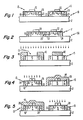
- the semiconductor device of the present invention includes source and drain regions formed in a layer of semiconductor material which is disposed on an insulating substrate.
- the source and drain regions each have a depth which is less than the thickness of the layer of semiconductor material.
- Source and drain depth extenders of the same conductivity type as the source and drain regions are formed in the layer of semiconductor material so that they have a common boundary with the insulating substrate.
- the present invention also includes a method of fabricating the semiconductor device described above.
- the N-channel transistor formed in the first silicon island 13 has a P-type region 14 disposed between N-type source and drain depth extenders 18 and 20, respectively.
- Heavily doped N-type source and drain regions 34 and 36, respectively, are disposed above the respective source and drain depth extenders 18 and 20.
- the source and drain regions 34 and 36, respectively, each have a depth which is less than the thickness of the first silicon island 13.
- the source and drain depth extenders 18 and 20, respectively have a common boundary with the sapphire substrate 12.
- FIGURE 1 also illustrates that the source and drain depth extenders 18 and 20, respectively, are separated by a distance which is greater than the channel length between the source and drain regions 34 and 36, respectively.
- the heavily doped source and drain regions 38 and 40 have a P-type impurity concentration which is about three orders of magnitude greater than the P-type impurity concentration of the respective source and drain depth extenders 22 and 24.
- the source and drain regions 38 and 40 will typically each have an impurity concentration of about 1020 cm ⁇ 3 while the source and drain depth extenders 18 and 20, respectively, each have an impurity concentration of about 1017 cm ⁇ 3.
- a gate oxide layer 28 and a gate electrode 32 are also provided on the second silicon island 15.
- the implant energies are controlled so that the self-aligned source and drain regions 34 and 36, respectively, each have a depth which is less than the thickness of the first silicon island 13.
- the source and drain regions have this limited depth because the implant energies are selected so that the dopant ions do not penetrate the gate electrode 30 and damage the underlying portion of the gate oxide layer 26.
- the second photoresist layer 44 is then removed using a conventional solvent.
- a method similar to that illustrated by FIGURES 3 to 5 is used to form the common island CMOS device 50 shown in FIGURE 2.
- the patterning step used to define the first photoresist layer 42 is modified so that the photoresist layer 42 overlies the regions of the silicon island 17 which correspond to the N-type source and drain depth extenders 18 and 20, respectively, and the N-type region 16.
- the second 44 and third 46 photoresist layers used in steps illustrated by FIGURES 4 and 5, respectively, are applied so they do not overlie the adjacent MOS transistor.
- FIGURES 3 to 5 utilizes N-type single-crystalline silicon as the island material, P-type single-crystalline silicon could also be used. In the latter case, the step illustrated by FIGURE 3 would be modified by using N-type dopants with a reverse image of the photoresist pattern shown.
- the present invention is also considered to include the formation of source and drain depth extenders in a single MOS transistor.
- Another embodiment of the present invention would include the use of intrinsic single-crystalline silicon as the island material.
- the step illustrated by FIGURE 3 would be carried out to form the P-type source and drain depth extenders 22 and 24, respectively, and the P-type region 14.
- the N-type source and drain depth extenders 18 and 20, respectively, would then be formed by implanting N-type dopants into the first silicon island 13 using a masking layer which is the reverse image of the first photoresist layer 42 shown overlying the first silicon island 13 in FIGURE 3.
- the P-type source and drain depth extenders 22 and 24, respectively are covered with a masking layer while the central region of the second silicon island 15 is exposed so that the N-type region 16 is formed.
- the damage to the gate oxide layer that occurs when high energy source and drain implants are performed in the conventional method in order to extend the source and drain regions to the insulating substrate is avoided with the method of the present invention.
- the high energy implant used in the present invention to form the source and drain depth extenders is carried out before the gate oxide layer is grown.
- silicon island thicknesses on the order of 5500 ⁇ or larger can be utilized.
- the thicker silicon island helps to ensure that good surface mobility will be present in the channel region of the MOS transistor.
- the source and drain implants are carried out in the present invention after the gate oxide and gate electrode are formed, only low energy implants are required since the source and drain region have a depth which is less than the silicon island thickness. Ions implanted at these energies will not pass through the gate electrode and damage the gate oxide.
- the back-channel length between the source and drain depth extenders is greater than the channel length between the source and drain regions. This longer back-channel provides for a higher series resistance between the source and drain regions. The higher series resistance helps to suppress radiation-induced back-channel leakage in N-channel transistors.
Landscapes
- Thin Film Transistor (AREA)
Priority Applications (1)
| Application Number | Priority Date | Filing Date | Title |
|---|---|---|---|
| DE19883886924 DE3886924T2 (de) | 1988-04-12 | 1988-04-12 | Halbleiterbauelement mit tiefen Source- und Drainerweiterungen sowie Verfahren zu seiner Herstellung. |
Applications Claiming Priority (1)
| Application Number | Priority Date | Filing Date | Title |
|---|---|---|---|
| US07/018,314 US4786955A (en) | 1987-02-24 | 1987-02-24 | Semiconductor device with source and drain depth extenders and a method of making the same |
Publications (2)
| Publication Number | Publication Date |
|---|---|
| EP0337020A1 true EP0337020A1 (fr) | 1989-10-18 |
| EP0337020B1 EP0337020B1 (fr) | 1994-01-05 |
Family
ID=21787305
Family Applications (1)
| Application Number | Title | Priority Date | Filing Date |
|---|---|---|---|
| EP88303277A Expired - Lifetime EP0337020B1 (fr) | 1987-02-24 | 1988-04-12 | Dispositif à semi-conducteur ayant des extentions profondes de la source du drain ainsi que le procédé pour sa fabrication |
Country Status (2)
| Country | Link |
|---|---|
| US (1) | US4786955A (fr) |
| EP (1) | EP0337020B1 (fr) |
Families Citing this family (15)
| Publication number | Priority date | Publication date | Assignee | Title |
|---|---|---|---|---|
| US4951113A (en) * | 1988-11-07 | 1990-08-21 | Xerox Corporation | Simultaneously deposited thin film CMOS TFTs and their method of fabrication |
| US5028556A (en) * | 1990-02-16 | 1991-07-02 | Hughes Aircraft Company | Process for fabricating radiation hard high voltage devices |
| US5272097A (en) * | 1992-04-07 | 1993-12-21 | Philip Shiota | Method for fabricating diodes for electrostatic discharge protection and voltage references |
| US5591661A (en) * | 1992-04-07 | 1997-01-07 | Shiota; Philip | Method for fabricating devices for electrostatic discharge protection and voltage references, and the resulting structures |
| US5315144A (en) * | 1992-09-18 | 1994-05-24 | Harris Corporation | Reduction of bipolar gain and improvement in snap-back sustaining voltage in SOI field effect transistor |
| US5719065A (en) | 1993-10-01 | 1998-02-17 | Semiconductor Energy Laboratory Co., Ltd. | Method for manufacturing semiconductor device with removable spacers |
| US6330217B1 (en) | 1995-06-16 | 2001-12-11 | Hewlett-Packard Company | Media cartridge insertion apparatus for a media cartridge storage and handling system |
| TW374196B (en) * | 1996-02-23 | 1999-11-11 | Semiconductor Energy Lab Co Ltd | Semiconductor thin film and method for manufacturing the same and semiconductor device and method for manufacturing the same |
| KR100344818B1 (ko) * | 1997-09-24 | 2002-11-18 | 주식회사 하이닉스반도체 | 반도체소자및그의제조방법 |
| US6686623B2 (en) | 1997-11-18 | 2004-02-03 | Semiconductor Energy Laboratory Co., Ltd. | Nonvolatile memory and electronic apparatus |
| JP2000012864A (ja) | 1998-06-22 | 2000-01-14 | Semiconductor Energy Lab Co Ltd | 半導体装置の作製方法 |
| US6271101B1 (en) | 1998-07-29 | 2001-08-07 | Semiconductor Energy Laboratory Co., Ltd. | Process for production of SOI substrate and process for production of semiconductor device |
| JP4476390B2 (ja) | 1998-09-04 | 2010-06-09 | 株式会社半導体エネルギー研究所 | 半導体装置の作製方法 |
| US7732287B2 (en) * | 2006-05-02 | 2010-06-08 | Honeywell International Inc. | Method of forming a body-tie |
| US7964897B2 (en) | 2008-07-22 | 2011-06-21 | Honeywell International Inc. | Direct contact to area efficient body tie process flow |
Citations (5)
| Publication number | Priority date | Publication date | Assignee | Title |
|---|---|---|---|---|
| DE2545871B2 (de) * | 1974-12-06 | 1980-06-19 | International Business Machines Corp., Armonk, N.Y. (V.St.A.) | Feldeffekttransistor mit verbesserter Stabilität der Schwellenspannung |
| US4276688A (en) * | 1980-01-21 | 1981-07-07 | Rca Corporation | Method for forming buried contact complementary MOS devices |
| US4335504A (en) * | 1980-09-24 | 1982-06-22 | Rockwell International Corporation | Method of making CMOS devices |
| EP0077737A2 (fr) * | 1981-10-19 | 1983-04-27 | FAIRCHILD CAMERA & INSTRUMENT CORPORATION | Dispositif à effet de champ à basse capacité |
| US4507846A (en) * | 1982-10-27 | 1985-04-02 | Tokyo Shibaura Denki Kabushiki Kaisha | Method for making complementary MOS semiconductor devices |
Family Cites Families (5)
| Publication number | Priority date | Publication date | Assignee | Title |
|---|---|---|---|---|
| US4393578A (en) * | 1980-01-02 | 1983-07-19 | General Electric Company | Method of making silicon-on-sapphire FET |
| JPS56147480A (en) * | 1980-04-18 | 1981-11-16 | Toshiba Corp | Semiconductor device and manufacture thereof |
| US4385937A (en) * | 1980-05-20 | 1983-05-31 | Tokyo Shibaura Denki Kabushiki Kaisha | Regrowing selectively formed ion amorphosized regions by thermal gradient |
| US4574467A (en) * | 1983-08-31 | 1986-03-11 | Solid State Scientific, Inc. | N- well CMOS process on a P substrate with double field guard rings and a PMOS buried channel |
| JPS61199665A (ja) * | 1985-03-01 | 1986-09-04 | Hitachi Ltd | 薄膜半導体装置 |
-
1987
- 1987-02-24 US US07/018,314 patent/US4786955A/en not_active Expired - Lifetime
-
1988
- 1988-04-12 EP EP88303277A patent/EP0337020B1/fr not_active Expired - Lifetime
Patent Citations (5)
| Publication number | Priority date | Publication date | Assignee | Title |
|---|---|---|---|---|
| DE2545871B2 (de) * | 1974-12-06 | 1980-06-19 | International Business Machines Corp., Armonk, N.Y. (V.St.A.) | Feldeffekttransistor mit verbesserter Stabilität der Schwellenspannung |
| US4276688A (en) * | 1980-01-21 | 1981-07-07 | Rca Corporation | Method for forming buried contact complementary MOS devices |
| US4335504A (en) * | 1980-09-24 | 1982-06-22 | Rockwell International Corporation | Method of making CMOS devices |
| EP0077737A2 (fr) * | 1981-10-19 | 1983-04-27 | FAIRCHILD CAMERA & INSTRUMENT CORPORATION | Dispositif à effet de champ à basse capacité |
| US4507846A (en) * | 1982-10-27 | 1985-04-02 | Tokyo Shibaura Denki Kabushiki Kaisha | Method for making complementary MOS semiconductor devices |
Non-Patent Citations (3)
| Title |
|---|
| IBM TECHNICAL DISCLOSURE BULLETIN * |
| JAPANESE JOURNAL OF APPLIED PHYSICS * |
| PATENT ABSTRACTS OF JAPAN * |
Also Published As
| Publication number | Publication date |
|---|---|
| US4786955A (en) | 1988-11-22 |
| EP0337020B1 (fr) | 1994-01-05 |
Similar Documents
| Publication | Publication Date | Title |
|---|---|---|
| US4717683A (en) | CMOS process | |
| EP0308295B1 (fr) | Procédé de fabrication de dispositifs CMOS | |
| US5346839A (en) | Sidewall doping technique for SOI transistors | |
| US5359219A (en) | Silicon on insulator device comprising improved substrate doping | |
| EP0031020B1 (fr) | Transistor à effet de champ DMOS et procédé de fabrication | |
| KR100199527B1 (ko) | 약하게 도핑된 드레인(ldd)형의 cmos장치제조방법 | |
| US4385947A (en) | Method for fabricating CMOS in P substrate with single guard ring using local oxidation | |
| US4797721A (en) | Radiation hardened semiconductor device and method of making the same | |
| US4402761A (en) | Method of making self-aligned gate MOS device having small channel lengths | |
| EP0575278A2 (fr) | Transistor à grille verticale avec un canal épitaxié à basse température | |
| WO1983003709A1 (fr) | Procede de formation de dispositifs de circuits integres complementaires | |
| US4786955A (en) | Semiconductor device with source and drain depth extenders and a method of making the same | |
| JPH0576190B2 (fr) | ||
| US4276688A (en) | Method for forming buried contact complementary MOS devices | |
| EP0442296B1 (fr) | Isolateur avec revêtement de silicone, à haute vitesse et son procédé de fabrication | |
| US4507846A (en) | Method for making complementary MOS semiconductor devices | |
| JPH07201974A (ja) | 半導体装置の製造方法 | |
| US4294002A (en) | Making a short-channel FET | |
| US4277882A (en) | Method of producing a metal-semiconductor field-effect transistor | |
| JP2997377B2 (ja) | 半導体装置及びその製造方法 | |
| EP0023528A1 (fr) | Structure de transistor à double diffusion et procédé pour sa fabrication | |
| US6080612A (en) | Method of forming an ultra-thin SOI electrostatic discharge protection device | |
| US6455405B1 (en) | Using implantation method to control gate oxide thickness on dual oxide semiconductor devices | |
| US4170500A (en) | Process for forming field dielectric regions in semiconductor structures without encroaching on device regions | |
| EP0514602B1 (fr) | Structure de canal MOSFET et sa méthode de fabrication |
Legal Events
| Date | Code | Title | Description |
|---|---|---|---|
| PUAI | Public reference made under article 153(3) epc to a published international application that has entered the european phase |
Free format text: ORIGINAL CODE: 0009012 |
|
| AK | Designated contracting states |
Kind code of ref document: A1 Designated state(s): DE FR IT NL |
|
| 17P | Request for examination filed |
Effective date: 19900320 |
|
| 17Q | First examination report despatched |
Effective date: 19920518 |
|
| GRAA | (expected) grant |
Free format text: ORIGINAL CODE: 0009210 |
|
| AK | Designated contracting states |
Kind code of ref document: B1 Designated state(s): DE FR IT NL |
|
| PG25 | Lapsed in a contracting state [announced via postgrant information from national office to epo] |
Ref country code: NL Effective date: 19940105 |
|
| REF | Corresponds to: |
Ref document number: 3886924 Country of ref document: DE Date of ref document: 19940217 |
|
| ITF | It: translation for a ep patent filed | ||
| EN | Fr: translation not filed | ||
| PG25 | Lapsed in a contracting state [announced via postgrant information from national office to epo] |
Ref country code: FR Effective date: 19940527 |
|
| NLV1 | Nl: lapsed or annulled due to failure to fulfill the requirements of art. 29p and 29m of the patents act | ||
| PLBE | No opposition filed within time limit |
Free format text: ORIGINAL CODE: 0009261 |
|
| STAA | Information on the status of an ep patent application or granted ep patent |
Free format text: STATUS: NO OPPOSITION FILED WITHIN TIME LIMIT |
|
| 26N | No opposition filed | ||
| REG | Reference to a national code |
Ref country code: FR Ref legal event code: RN |
|
| EN | Fr: translation not filed |
Free format text: BO 94/21 DU 940527: "LA MENTION DU DEFAUT DE LA REMISE DE LA TRADUCTION EST A CONSIDERER COMME NULLE ET NON AVENUE" |
|
| ET | Fr: translation filed | ||
| PGFP | Annual fee paid to national office [announced via postgrant information from national office to epo] |
Ref country code: FR Payment date: 19970318 Year of fee payment: 10 |
|
| PGFP | Annual fee paid to national office [announced via postgrant information from national office to epo] |
Ref country code: DE Payment date: 19970324 Year of fee payment: 10 |
|
| PG25 | Lapsed in a contracting state [announced via postgrant information from national office to epo] |
Ref country code: DE Free format text: LAPSE BECAUSE OF NON-PAYMENT OF DUE FEES Effective date: 19990202 |
|
| PG25 | Lapsed in a contracting state [announced via postgrant information from national office to epo] |
Ref country code: IT Free format text: LAPSE BECAUSE OF NON-PAYMENT OF DUE FEES Effective date: 20050412 |