EP0337676A2 - Réseau logique programmable - Google Patents
Réseau logique programmable Download PDFInfo
- Publication number
- EP0337676A2 EP0337676A2 EP89303460A EP89303460A EP0337676A2 EP 0337676 A2 EP0337676 A2 EP 0337676A2 EP 89303460 A EP89303460 A EP 89303460A EP 89303460 A EP89303460 A EP 89303460A EP 0337676 A2 EP0337676 A2 EP 0337676A2
- Authority
- EP
- European Patent Office
- Prior art keywords
- programmable logic
- logic array
- sub
- array
- clock signal
- Prior art date
- Legal status (The legal status is an assumption and is not a legal conclusion. Google has not performed a legal analysis and makes no representation as to the accuracy of the status listed.)
- Granted
Links
Images




Classifications
-
- H—ELECTRICITY
- H03—ELECTRONIC CIRCUITRY
- H03K—PULSE TECHNIQUE
- H03K19/00—Logic circuits, i.e. having at least two inputs acting on one output; Inverting circuits
- H03K19/02—Logic circuits, i.e. having at least two inputs acting on one output; Inverting circuits using specified components
- H03K19/173—Logic circuits, i.e. having at least two inputs acting on one output; Inverting circuits using specified components using elementary logic circuits as components
- H03K19/177—Logic circuits, i.e. having at least two inputs acting on one output; Inverting circuits using specified components using elementary logic circuits as components arranged in matrix form
-
- H—ELECTRICITY
- H03—ELECTRONIC CIRCUITRY
- H03K—PULSE TECHNIQUE
- H03K19/00—Logic circuits, i.e. having at least two inputs acting on one output; Inverting circuits
- H03K19/0008—Arrangements for reducing power consumption
- H03K19/0016—Arrangements for reducing power consumption by using a control or a clock signal, e.g. in order to apply power supply
-
- H—ELECTRICITY
- H03—ELECTRONIC CIRCUITRY
- H03K—PULSE TECHNIQUE
- H03K19/00—Logic circuits, i.e. having at least two inputs acting on one output; Inverting circuits
- H03K19/02—Logic circuits, i.e. having at least two inputs acting on one output; Inverting circuits using specified components
- H03K19/173—Logic circuits, i.e. having at least two inputs acting on one output; Inverting circuits using specified components using elementary logic circuits as components
- H03K19/177—Logic circuits, i.e. having at least two inputs acting on one output; Inverting circuits using specified components using elementary logic circuits as components arranged in matrix form
- H03K19/17704—Logic circuits, i.e. having at least two inputs acting on one output; Inverting circuits using specified components using elementary logic circuits as components arranged in matrix form the logic functions being realised by the interconnection of rows and columns
- H03K19/17708—Logic circuits, i.e. having at least two inputs acting on one output; Inverting circuits using specified components using elementary logic circuits as components arranged in matrix form the logic functions being realised by the interconnection of rows and columns using an AND matrix followed by an OR matrix, i.e. programmable logic arrays
- H03K19/17716—Logic circuits, i.e. having at least two inputs acting on one output; Inverting circuits using specified components using elementary logic circuits as components arranged in matrix form the logic functions being realised by the interconnection of rows and columns using an AND matrix followed by an OR matrix, i.e. programmable logic arrays with synchronous operation, i.e. using clock signals, e.g. of I/O or coupling register
- H03K19/1772—Logic circuits, i.e. having at least two inputs acting on one output; Inverting circuits using specified components using elementary logic circuits as components arranged in matrix form the logic functions being realised by the interconnection of rows and columns using an AND matrix followed by an OR matrix, i.e. programmable logic arrays with synchronous operation, i.e. using clock signals, e.g. of I/O or coupling register with synchronous operation of at least one of the logical matrixes
Definitions
- the present invention generally relates to a programmable logic array, and more particularly to a reduction in power consumed in a programmable logic array.
- a programmable logic array (hereafter simply referred to as a PLA) is a circuit in which a desired logical function can be programed.
- a PLA has such a structure that circuit elements are regularly arranged as conventional memories.
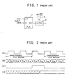
- a PLA 1 includes an OR array and an AND array, each of which includes precharge transistors and discharge transistors.
- a clock signal CLK as shown in FIG.2(A) is applied to the PLA 1.
- the clock signal CLK is held at a high level (hereafter simply referred to H level)
- the PLA 1 is precharged.
- the clock signal CLK is held at a low level (hereafter simply referred to as L level)
- the PLA 1 is discharged. Therefore, the state of the PLA changes as shown in FIG.2(B) where "Pre” indicates a precharged state, and "Dis” indicates a discharged state.
- the PLA 1 enters data supplied to an input data terminal IN thereof in the precharged state, and outputs a logic output to a latch circuit 2 in the discharged state.
- An AND gate 3 makes an AND operation on an inverted clock pulse signal CLK and a read signal RD as shown in FIG.2(C), and generates a control signal.
- the latch circuit 2 latches a logic output from the PLA 1 at the rise of the inverted clock pulse signal CLK . Therefore, the output signal of the latch circuit 2 changes with a timing as shown in FIG.2(D).
- the precharging and discharging are alternately carried out all the time.
- the PLA 1 is always accessed, or in other words, the PLA 1 is accessed during a time even when it is not required to read data from the PLA 1.
- the above-mentioned access operation is wasteful of power, since current passes through discharge transistors during discharge periods even when the PLA 1 is not accessed.
- PLAs are fabricated as large scale integrated circuits. Therefore, it is particularly desired that power consumption is as low as possible.
- a PLA is divided into a plurality of blocks (sub-PLAs).
- a divided block to be selected is supplied with power, and the remaining blocks (which are not selected) are supplied with no power.
- ON/OFF switches are interposed between a power source line and the divided blocks of the PLA.
- a divided block of an OR array which is not selected at present, is inhibited from being precharged.
- a more specific object of the present invention is to provide a programmable logic array with reduced power consumption and higher speed.
- a programmable logic array comprising a programmable logic array being precharged and discharged in synchronism with a clock signal supplied thereto and outputting an operation result with respect to input data supplied thereto; and means connected to the programmable logic array, for holding the programmable logic array in a precharged state by setting the clock signal to a fixed level when the programmable logic array is not selected and for switching the programmable logic array to a discharged state by supplying the clock signal the programmable logic array when the programmable logic array is selected, so that the programmable logic array is discharged on the basis of the contents of the input data when selected.
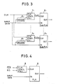
- the illustrated PLA includes a plurality of sub-PLAs 51 through 5 n , which are formed by dividing a PLA into portions, depending on functions.
- Decoders 61 through 6 n which are provided with corresponding sub-PLAs 51 through 5 n , determine whether or not the corresponding sub-PLAs 51 through 5 n are selected based on input data supplied thereto.
- Clock control circuits 71 through 7 n associated with the sub-PLAs 51 through 5 n are provided with output signals of the decoders 61 through 6 n and a clock pulse signal CLK shown in FIG.5(A).
- the clock control circuits 71 through 7 n generate corresponding clock pulse signals CLK1 through CLKn (FIG.5(B)), which are to be supplied to clock input terminals CLK of the corresponding sub-PLAs 51 through 5 n , only when the clock control circuits 71 through 7 n determine that the corresponding sub-PLAs 51 through 5 n are selected.
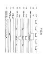
- input data includes information on functions to be executed as shown in FIG.5(H).
- Functions #1, #2 and #n relate to the sub-PLA 51, 52 and 5 n , respectively.
- the decoder 61 outputs a control signal to activate the clock control circuit 71 associated with the sub-PLA 51.
- the clock control circuit 71 generates the clock pulse signal CLK1 by simply passing through the clock pulse signal CLK supplied thereto.
- the sub PLA 51 is alternately switched to the precharged state and discharged state in synchronism with the clock pulse signal CLK1, as shown in FIG.5(C).
- the clock control circuit 71 holds the level of the clock pulse signal CLK1 high.
- the PLA 51 is kept in the precharged state, as shown in FIG.5(C).
- the sub-PLA 51 is kept in the precharged state.
- the other sub-PLAs 52 through 5 n operate in the same way as the sub-PLA 51. It is noted that each of the sub-PLAs 51 through 5 n is alternately switched to the discharged and precharged states only when it is selected, and is kept in the precharged state when not selected. As a result, it is possible to reduce power consumption resulting from current passing through discharge transistors during non-selected state. In the structure of FIG.3, the sub-PLA 51 through 5 n are periodically selected.
- a PLA 9 is not divided into sub-PLAs. That is, a conventional PLA is used as it is.
- a clock input terminal of the PLA 9 is connected to a clock control circuit 8, to which the clock pulse signal CLK and read signal RD are supplied, as shown in FIGS.6(A) and 6(D), respectively.
- the clock control circuit switches the output thereof to L level in synchronism with the rise of the clock pulse signal CLK .
- Input data is supplied to an input data terminal IN of the PLA 9.
- the PLA 9 is discharged only when the read signal RD is active (H level), and is kept in the precharged state during a time when the read signal RD is kept at L level.
- PLAs and sub-PLAs are kept in the precharged state during the time when they are not selected. Reason for the above will be described in detail later.
- the illustrated embodiment of the present invention is based on combination of FIGS.3 and 5.
- a PLA 11 has an input of 28 bits, an output of 23 bits, and 1653 product term lines. Functions available by the PLA 11 are divided into 10 functions of A through J, as shown in FIG.9. The available functions A through J are achieved by divided 13 sub PLAs 51 through 513, each of which includes 131 product terms.
- the sub-PLA 52 is composed of 27 product terms relating to function A, and 104 product terms relating to function B. Functions A and B achieved by the sub-PLA 52 can be separately selected. When function A is designated, both the PLAs 51 and 52 are selected.
- the sub-PLA 53 includes 28 product terms relating to function B, and 103 product terms relating to function C.
- the clock input terminals CLK of the sub-PLAs 51 through 513 are connected to output terminals of corresponding 3-input NAND gates 121 through 1213.
- Each of the NAND gates 121 through 1213 is supplied with the clock pulse signal CLK and the read signal RD.
- the remaining input terminals of the NAND gates 121 through 1213 are connected to the output terminals of the corresponding decoders 61 through 613.
- the decoders 61 through 613 are supplied with 6 bits out of the 28-bit input data to be supplied to the input data terminals IN of the sub-PLAs. 51 through 513.
- Output terminals OUT of the sub-PLAs 51 through 513 are connected to gates of n-channel metal oxide semiconductor (MOS) transistors 141 through 1413 through inverters 131 through 1313, respectively.
- the NAND gates 121 through 1213 generate clock pulse signals CLK1 through CLK13, respectively.
- the sources of the MOS transistors 141 through 1413 are connected to ground (a negative power source), and drains thereof are mutually connected to thereby form a wired OR logic.
- the drains of the MOS transistors 141 through 1413 are connected to a precharge circuit 16.
- FIG.7B is a circuit diagram of the precharge circuit 16 and its peripheral circuit.
- the precharge circuit 16 is made up of n-channel MOS transistors 16a, 16b, and a p-channel MOS transistor 16c.
- a clock control circuit 61′ has a function identical to the clock control circuit 8 shown in FIG.4.
- the output terminal of the clock control circuit 61′ is connected to the gate of the MOS transistor 16a, and the gate of the MOS transistor 16c through an inverter 16d.
- the source of the MOS transistor 16a and the drain of the MOS transistor 16c are coupled to each other through the MOS transistor 16b.
- the drain of the MOS transistor 16c is coupled to an external terminal EXT of the PLA 11 through an inverter 16e.
- the output terminal EXT of the PLA 11 is connected to the latch circuit 2, which is controlled by the AND gate 3.
- the latch circuit 2 and NAND gate 3 shown in FIG.7A are the same as those shown in FIG.1.
- FIG.10A illustrates an example of the internal structure for each of the sub-PLAs 5 through 513.
- the input data is supplied to an AND array 51 through an AND array driver 52, which includes a plurality of precharge transistors TRp and discharge transistors TRd.
- the precharge and discharge transistors TRp and TRd are of p- and n-channels, respectively.
- OR array drivers 54 of conventional type.
- Each of the OR array drivers 54 is made up of an n-channel MOS transistor 541, and p-channel MOS transistors 542 and 543.
- the equivalent circuit of each of the OR array drivers 54 is illustrated in FIG.10B.
- Each OR array driver 54 is composed of an NAND gate 544 and an inverter 545.
- Input lines 51a extending from the AND array driver 52 are connected to gates of the corresponding discharge transistors TRd.
- a timing circuit 53 is made up of a precharge transistor TRp1 and a discharge transistor TRd1, which are connected to a control line 51e.
- the control line 51e is coupled to the gates of the transistors 542 of the OR array drivers 54 through inverters INV1, INV2 and INV3.
- the control line 51e is also coupled to the sources of the transistors 541 of the OR array drivers 54 through the inverters INV1 and INV2.
- Product term lines 55c extending from the OR array drivers 54 are connected to gates of discharge transistors TRd′ of n-channel MOS transistors provided in an OR array 55.
- the product term lines 55c are also connected to drains of n-channel MOS transistors 551.
- the output terminal of the inverter INV3 is connected to the gates of precharge transistors TRp′ and an inverter 552.
- the output terminal of the inverter INV 552 is connected to the gates of the transistors 551.
- Output lines 55a extend from the precharge transistors TRp′, to which discharge transistors TRd′ are connected, as shown in FIG.10A.
- the read signal RD is held at L level, and therefore the clock pulse signal CLKi derived from the NAND gates 12i is held at H level, as shown in FIGS.8(B), 8(D) and 8(H).
- the gates of the precharge transistors TRp and TRp′ shown in FIG.10A are set to L level, and therefore these transistors are turned ON.
- the product term lines 51c and the control line 51e are precharged up to the positive power source voltage Vcc (H level).
- the H level of the control line 51e is transferred to the inverters INV1 through INV3, and therefore the inverter INV3 outputs L level.
- This L level is supplied to the precharge transistors TRp′.
- the L level obtained at the output of the inverter INV3 is applied to the gates of the transistors 542 of the OR array drivers 54. Therefore, the outputs of the transistors 542 are switched to H level, and accordingly the transistors 543 are turned OFF. As a result, the outputs of the transistors 543 become the floating state.
- the transistors 551 since the output of the inverter 552 is held at H level, the transistors 551 are turned ON, and therefore the lines 55c are switched to L level.
- the product term lines 55c in the OR array 55 are set to L level, and thereby the discharge transistors TRd′ are kept OFF. In this way, the output lines 55a are pr′charged to H level, and all the sub-PLAs 51 through 513 are held in the precharged state.
- the read signal RD is switched to H level, and the input data becomes indicative of function B as shown in FIG.8(C).
- the input data relating to function B is decoded by the decoder 62, which generates the control signal to be supplied to the NAND gate 122.
- the NAND gate 122 generates the clock pulse signal CLK2 as shown in FIG.8(D).
- the sub-PLA 52 is switched to the discharged state.
- discharge transistors TRd of the sub-PLA 52 relating to the input data are turned ON based on the contents of the input data, and related product term lines in the AND array 52 are discharged, as shown in 8(E). Further, output lines 55a relating to the discharged product term lines 51c are discharged through the corresponding discharge transistors TRd′ in the OR array 55 of the sub-PLA 52.
- the input data is decoded by the decoder 63 relating to function B, which generates the control signal to be supplied to the NAND gate 123, as shown in FIG.8(F). Then, the discharge transistors TRd of the sub-PLA 53 to the input data are turned ON, and related product term lines in the AND array 52 are discharged, as shown in 8(E). Further, output lines 55a relating to the discharge product term lines 55c are discharged through the corresponding discharge transistors TRd′ of the sub-PLA 53.
- the output signals of the sub-PLAs 52 and 53 are transferred to the latch circuit 2 through the inverters 132, 133, transistors 142, 143, and the precharge circuit 16. During this operation, the output signal of the PLAs 52 and 53 are inverted, and are then output to the latch circuit 2. Then the latch circuit 2 latches the output signal of the PLA 11 with a timing when both the read signal RD and the clock pulse signal CLK are held at H level.
- the remaining decoders 61 and 64 through 613 generate no control signal. Therefore, the sub-PLAs 51, and 54 through 513 are kept in the precharged state.
- PLAs or sub-PLAs which are not selected are held in the precharged state. If the PLA shown in FIG.4 is designed so as to start precharging when the read signal RD is supplied to the clock control circuit 8, a sufficient precharging time may be not obtained due to a delay of the read signal RD from the rise of the clock signal CLK . If the PLA is not sufficiently precharged, an error in reading data may occur. In order to prevent the occurrence of error, the precharging must be done in synchronism with the next rise of the clock signal CLK. This leads to a delay of read operation. On the other hand, according to the aforementioned embodiment, currently selected sub-PLAs among the sub-PLAs 51 through 513 are held in the precharged state. Therefore, even when there exists some delay of time, data can be read out correctly when the read signal RD occurs.
- FIG.11A is an example of the configuration for the decoder 61.
- the decoder 61 is made up of inverters INV10 through INV15 and an AND gate 61.
- FIG.11B is an example of the configuration for the decoder 62.
- the decoder 62 is made up of inverters INV16 through INV20, and an AND gate 62.
- the sub-PLA 52 has functions A and B. Therefore, all of the bits S0 through S4 are zero, the AND gate 62 generates the control signal to be supplied to the NAND gate 122 shown in FIG.7A.
- power consumption is reduced as small as one-thirteenth power consumption of the conventional PLA shown in FIG.1.
- each of the sub-PLAs 51 through 513 is carried out for every m cycles, it is possible to reduce power consumption as small as approximately (1/13m).
- FIG.7A has been described as a preferred embodiment, the structure of FIG.3 or FIG.5 is also effective to reduce power consumption.
Landscapes
- Physics & Mathematics (AREA)
- Mathematical Physics (AREA)
- Engineering & Computer Science (AREA)
- Computer Hardware Design (AREA)
- Computing Systems (AREA)
- General Engineering & Computer Science (AREA)
- Logic Circuits (AREA)
- Power Sources (AREA)
Applications Claiming Priority (2)
| Application Number | Priority Date | Filing Date | Title |
|---|---|---|---|
| JP63088592A JP2547436B2 (ja) | 1988-04-11 | 1988-04-11 | Pla制御方式 |
| JP88592/88 | 1988-04-11 |
Publications (3)
| Publication Number | Publication Date |
|---|---|
| EP0337676A2 true EP0337676A2 (fr) | 1989-10-18 |
| EP0337676A3 EP0337676A3 (en) | 1990-06-27 |
| EP0337676B1 EP0337676B1 (fr) | 1995-01-11 |
Family
ID=13947105
Family Applications (1)
| Application Number | Title | Priority Date | Filing Date |
|---|---|---|---|
| EP89303460A Expired - Lifetime EP0337676B1 (fr) | 1988-04-11 | 1989-04-07 | Réseau logique programmable |
Country Status (5)
| Country | Link |
|---|---|
| US (1) | US5033017A (fr) |
| EP (1) | EP0337676B1 (fr) |
| JP (1) | JP2547436B2 (fr) |
| KR (1) | KR930002258B1 (fr) |
| DE (1) | DE68920467T2 (fr) |
Cited By (6)
| Publication number | Priority date | Publication date | Assignee | Title |
|---|---|---|---|---|
| EP0428300A3 (en) * | 1989-11-13 | 1991-08-14 | Advanced Micro Devices, Inc. | Programmable logic array apparatus |
| US5329178A (en) * | 1991-11-27 | 1994-07-12 | North American Philips Corporation | Integrated circuit device with user-programmable conditional power-down means |
| EP0602421A3 (fr) * | 1992-12-17 | 1995-03-29 | Ibm | Réseaux logiques programmables à haute performance et à faible consommation. |
| EP0645700A3 (fr) * | 1993-09-29 | 1996-05-01 | Toshiba Kk | Réseau logique programmable. |
| US5757206A (en) * | 1991-11-27 | 1998-05-26 | Philips Electronics North America Corp. | Electronic circuit with programmable gradual power consumption control |
| EP0772878A4 (fr) * | 1995-05-26 | 1999-01-13 | Nat Semiconductor Corp | Circuit decodeur cloisonne pour fonctionnement basse puissance |
Families Citing this family (8)
| Publication number | Priority date | Publication date | Assignee | Title |
|---|---|---|---|---|
| JPH04211147A (ja) * | 1990-02-26 | 1992-08-03 | Nec Corp | ダイナミック型論理回路 |
| JP2544027B2 (ja) * | 1990-05-24 | 1996-10-16 | 株式会社東芝 | 低消費電力型プログラマブルロジックアレイおよびそれを用いた情報処理装置 |
| US5717344A (en) * | 1996-02-20 | 1998-02-10 | International Business Machines Corporation | PLA late signal circuitry using a specialized gap cell and PLA late signal circuitry using switched output |
| US5867038A (en) * | 1996-12-20 | 1999-02-02 | International Business Machines Corporation | Self-timed low power ratio-logic system having an input sensing circuit |
| US6492835B2 (en) * | 1998-01-09 | 2002-12-10 | Jeng-Jye Shau | Power saving methods for programmable logic arrays |
| US6425077B1 (en) * | 1999-05-14 | 2002-07-23 | Xilinx, Inc. | System and method for reading data from a programmable logic device |
| US8661394B1 (en) | 2008-09-24 | 2014-02-25 | Iowa State University Research Foundation, Inc. | Depth-optimal mapping of logic chains in reconfigurable fabrics |
| US8438522B1 (en) | 2008-09-24 | 2013-05-07 | Iowa State University Research Foundation, Inc. | Logic element architecture for generic logic chains in programmable devices |
Family Cites Families (15)
| Publication number | Priority date | Publication date | Assignee | Title |
|---|---|---|---|---|
| US3896418A (en) * | 1971-08-31 | 1975-07-22 | Texas Instruments Inc | Synchronous multi-processor system utilizing a single external memory unit |
| JPS52137229A (en) * | 1976-05-12 | 1977-11-16 | Hitachi Ltd | Programmable logic array |
| JPS52137228A (en) * | 1976-05-12 | 1977-11-16 | Hitachi Ltd | Programmable logic array |
| JPS5469040A (en) * | 1977-11-11 | 1979-06-02 | Sharp Corp | Driving system for c-mos circuit |
| JPS54109872A (en) * | 1978-02-17 | 1979-08-28 | Hitachi Ltd | Pla system of electronic type multifunction watch |
| US4317180A (en) * | 1979-12-26 | 1982-02-23 | Texas Instruments Incorporated | Clocked logic low power standby mode |
| JPS5775335A (en) * | 1980-10-27 | 1982-05-11 | Hitachi Ltd | Data processor |
| DE3166989D1 (en) * | 1980-10-29 | 1984-12-06 | Bbc Brown Boveri & Cie | Resonant chamber atomiser for liquids |
| JPS59208944A (ja) * | 1983-05-13 | 1984-11-27 | Hitachi Ltd | 半導体集積回路装置 |
| JPS60108953A (ja) * | 1983-11-15 | 1985-06-14 | モトローラ・インコーポレーテツド | メモリデータバスの多重化方法 |
| JPS6326716A (ja) * | 1986-07-18 | 1988-02-04 | Nec Ic Microcomput Syst Ltd | 中央処理装置 |
| JP2554475B2 (ja) * | 1986-09-11 | 1996-11-13 | 株式会社リコー | プログラマブル・ロジツク・デバイス |
| US4721868A (en) * | 1986-09-23 | 1988-01-26 | Advanced Micro Devices, Inc. | IC input circuitry programmable for realizing multiple functions from a single input |
| FR2611099B1 (fr) * | 1987-02-12 | 1993-02-12 | Bull Sa | Reseau logique dynamique |
| US4831285A (en) * | 1988-01-19 | 1989-05-16 | National Semiconductor Corporation | Self precharging static programmable logic array |
-
1988
- 1988-04-11 JP JP63088592A patent/JP2547436B2/ja not_active Expired - Lifetime
-
1989
- 1989-04-06 US US07/333,939 patent/US5033017A/en not_active Expired - Fee Related
- 1989-04-07 DE DE68920467T patent/DE68920467T2/de not_active Expired - Fee Related
- 1989-04-07 EP EP89303460A patent/EP0337676B1/fr not_active Expired - Lifetime
- 1989-04-10 KR KR1019890004716A patent/KR930002258B1/ko not_active Expired - Fee Related
Cited By (8)
| Publication number | Priority date | Publication date | Assignee | Title |
|---|---|---|---|---|
| EP0428300A3 (en) * | 1989-11-13 | 1991-08-14 | Advanced Micro Devices, Inc. | Programmable logic array apparatus |
| US5329178A (en) * | 1991-11-27 | 1994-07-12 | North American Philips Corporation | Integrated circuit device with user-programmable conditional power-down means |
| US5757206A (en) * | 1991-11-27 | 1998-05-26 | Philips Electronics North America Corp. | Electronic circuit with programmable gradual power consumption control |
| EP0602421A3 (fr) * | 1992-12-17 | 1995-03-29 | Ibm | Réseaux logiques programmables à haute performance et à faible consommation. |
| EP0645700A3 (fr) * | 1993-09-29 | 1996-05-01 | Toshiba Kk | Réseau logique programmable. |
| US5672984A (en) * | 1993-09-29 | 1997-09-30 | Kabushiki Kaisha Toshiba | Programmable logic array having power-saving banks |
| EP0772878A4 (fr) * | 1995-05-26 | 1999-01-13 | Nat Semiconductor Corp | Circuit decodeur cloisonne pour fonctionnement basse puissance |
| KR100403403B1 (ko) * | 1995-05-26 | 2004-03-26 | 내셔널 세미콘덕터 코포레이션 | 저전력 동작용 구분 디코더 회로 |
Also Published As
| Publication number | Publication date |
|---|---|
| KR930002258B1 (ko) | 1993-03-27 |
| JP2547436B2 (ja) | 1996-10-23 |
| DE68920467D1 (de) | 1995-02-23 |
| JPH01260924A (ja) | 1989-10-18 |
| EP0337676B1 (fr) | 1995-01-11 |
| US5033017A (en) | 1991-07-16 |
| KR890016666A (ko) | 1989-11-29 |
| DE68920467T2 (de) | 1995-06-01 |
| EP0337676A3 (en) | 1990-06-27 |
Similar Documents
| Publication | Publication Date | Title |
|---|---|---|
| US5033017A (en) | Programmable logic array with reduced power consumption | |
| JPH0628888A (ja) | 半導体記憶装置 | |
| JPH0652685A (ja) | パワーオンリセット制御型ラッチ型行ラインリピータを有する半導体メモリ | |
| JPH07111084A (ja) | 半導体集積回路装置 | |
| GB2325322A (en) | A high speed and low power signal line driver and semiconductor memory device using the same | |
| US4893033A (en) | Programmable logic array having input transition detection for generating precharge | |
| US3962686A (en) | Memory circuit | |
| US6088292A (en) | Semiconductor memory device having a plurality of banks activated by a common timing control circuit | |
| US6870776B2 (en) | Data output circuit in combined SDR/DDR semiconductor memory device | |
| US5636161A (en) | Eprom bit-line interface for implementing programming, verification and testing | |
| US5311479A (en) | Semiconductor memory device having a CMOS decoding circuit | |
| JPH01198120A (ja) | デコーダ回路 | |
| KR20030043944A (ko) | 플래시 메모리의 워드 라인 디코딩 구조 | |
| EP0342592B1 (fr) | Circuit d'entrée de signal d'autorisation de puce dans un dispositif de mémoire à semi-conducteurs | |
| US6111792A (en) | Non-volatile semiconductor memory device for selective cell flash erasing/programming | |
| JP2588936B2 (ja) | 半導体記憶装置 | |
| US6134177A (en) | Redundancy decoding circuit having automatic deselection | |
| US5394375A (en) | Row decoder for driving word line at a plurality of points thereof | |
| JPH06215595A (ja) | 半導体記憶装置 | |
| US6266293B1 (en) | Semiconductor memory device | |
| KR20000074505A (ko) | 로직 인터페이스 회로 및 이를 이용한 반도체 메모리 장치 | |
| EP0191699B1 (fr) | Schéma pour isoler une ligne de bit d'un amplificateur de lecture | |
| US5012451A (en) | ROM circuit | |
| KR950004863B1 (ko) | Eprom 래치회로 | |
| US6657912B1 (en) | Circuit for optimizing power consumption and performance |
Legal Events
| Date | Code | Title | Description |
|---|---|---|---|
| PUAI | Public reference made under article 153(3) epc to a published international application that has entered the european phase |
Free format text: ORIGINAL CODE: 0009012 |
|
| AK | Designated contracting states |
Kind code of ref document: A2 Designated state(s): DE FR GB |
|
| PUAL | Search report despatched |
Free format text: ORIGINAL CODE: 0009013 |
|
| AK | Designated contracting states |
Kind code of ref document: A3 Designated state(s): DE FR GB |
|
| 17P | Request for examination filed |
Effective date: 19901128 |
|
| 17Q | First examination report despatched |
Effective date: 19920917 |
|
| RAP1 | Party data changed (applicant data changed or rights of an application transferred) |
Owner name: FUJITSU DEVICES INC Owner name: FUJITSU LIMITED |
|
| GRAA | (expected) grant |
Free format text: ORIGINAL CODE: 0009210 |
|
| AK | Designated contracting states |
Kind code of ref document: B1 Designated state(s): DE FR GB |
|
| REF | Corresponds to: |
Ref document number: 68920467 Country of ref document: DE Date of ref document: 19950223 |
|
| ET | Fr: translation filed | ||
| PLBE | No opposition filed within time limit |
Free format text: ORIGINAL CODE: 0009261 |
|
| STAA | Information on the status of an ep patent application or granted ep patent |
Free format text: STATUS: NO OPPOSITION FILED WITHIN TIME LIMIT |
|
| 26N | No opposition filed | ||
| PGFP | Annual fee paid to national office [announced via postgrant information from national office to epo] |
Ref country code: GB Payment date: 19980330 Year of fee payment: 10 |
|
| PGFP | Annual fee paid to national office [announced via postgrant information from national office to epo] |
Ref country code: FR Payment date: 19980409 Year of fee payment: 10 |
|
| PGFP | Annual fee paid to national office [announced via postgrant information from national office to epo] |
Ref country code: DE Payment date: 19980414 Year of fee payment: 10 |
|
| PG25 | Lapsed in a contracting state [announced via postgrant information from national office to epo] |
Ref country code: GB Free format text: LAPSE BECAUSE OF NON-PAYMENT OF DUE FEES Effective date: 19990407 |
|
| GBPC | Gb: european patent ceased through non-payment of renewal fee |
Effective date: 19990407 |
|
| PG25 | Lapsed in a contracting state [announced via postgrant information from national office to epo] |
Ref country code: FR Free format text: LAPSE BECAUSE OF NON-PAYMENT OF DUE FEES Effective date: 19991231 |
|
| REG | Reference to a national code |
Ref country code: FR Ref legal event code: ST |
|
| PG25 | Lapsed in a contracting state [announced via postgrant information from national office to epo] |
Ref country code: DE Free format text: LAPSE BECAUSE OF NON-PAYMENT OF DUE FEES Effective date: 20000201 |