EP0337699B1 - Composition d'oxyde isolant utilisée dans un élément supraconducteur - Google Patents
Composition d'oxyde isolant utilisée dans un élément supraconducteur Download PDFInfo
- Publication number
- EP0337699B1 EP0337699B1 EP89303514A EP89303514A EP0337699B1 EP 0337699 B1 EP0337699 B1 EP 0337699B1 EP 89303514 A EP89303514 A EP 89303514A EP 89303514 A EP89303514 A EP 89303514A EP 0337699 B1 EP0337699 B1 EP 0337699B1
- Authority
- EP
- European Patent Office
- Prior art keywords
- composition
- superconductive
- insulating
- oxide
- insulating layer
- Prior art date
- Legal status (The legal status is an assumption and is not a legal conclusion. Google has not performed a legal analysis and makes no representation as to the accuracy of the status listed.)
- Expired - Lifetime
Links
- 239000000203 mixture Substances 0.000 title claims description 58
- 229910052760 oxygen Inorganic materials 0.000 claims description 42
- 239000002887 superconductor Substances 0.000 claims description 37
- 239000000758 substrate Substances 0.000 claims description 26
- 229910052802 copper Inorganic materials 0.000 claims description 25
- 238000000034 method Methods 0.000 claims description 23
- QVGXLLKOCUKJST-UHFFFAOYSA-N atomic oxygen Chemical compound [O] QVGXLLKOCUKJST-UHFFFAOYSA-N 0.000 claims description 20
- 229910052797 bismuth Inorganic materials 0.000 claims description 20
- WMWLMWRWZQELOS-UHFFFAOYSA-N bismuth(iii) oxide Chemical compound O=[Bi]O[Bi]=O WMWLMWRWZQELOS-UHFFFAOYSA-N 0.000 claims description 20
- 239000001301 oxygen Substances 0.000 claims description 20
- 229910052712 strontium Inorganic materials 0.000 claims description 20
- 230000007547 defect Effects 0.000 claims description 15
- 239000013078 crystal Substances 0.000 claims description 14
- 229910052745 lead Inorganic materials 0.000 claims description 11
- 229910052779 Neodymium Inorganic materials 0.000 claims description 7
- 229910052791 calcium Inorganic materials 0.000 claims description 7
- 229910052692 Dysprosium Inorganic materials 0.000 claims description 6
- 229910052691 Erbium Inorganic materials 0.000 claims description 6
- 229910052689 Holmium Inorganic materials 0.000 claims description 6
- 229910052765 Lutetium Inorganic materials 0.000 claims description 6
- 229910052772 Samarium Inorganic materials 0.000 claims description 6
- 229910052771 Terbium Inorganic materials 0.000 claims description 6
- 229910052775 Thulium Inorganic materials 0.000 claims description 6
- 229910052769 Ytterbium Inorganic materials 0.000 claims description 6
- 229910052693 Europium Inorganic materials 0.000 claims description 5
- 229910052688 Gadolinium Inorganic materials 0.000 claims description 5
- 238000007716 flux method Methods 0.000 claims description 5
- 229910052727 yttrium Inorganic materials 0.000 claims description 5
- 229910052788 barium Inorganic materials 0.000 claims description 3
- 230000004907 flux Effects 0.000 claims description 2
- 150000002500 ions Chemical class 0.000 claims description 2
- 239000002994 raw material Substances 0.000 claims description 2
- 229910052716 thallium Inorganic materials 0.000 claims description 2
- QPLDLSVMHZLSFG-UHFFFAOYSA-N Copper oxide Chemical compound [Cu]=O QPLDLSVMHZLSFG-UHFFFAOYSA-N 0.000 description 18
- 239000010408 film Substances 0.000 description 18
- 239000000843 powder Substances 0.000 description 10
- 230000000694 effects Effects 0.000 description 7
- LEDMRZGFZIAGGB-UHFFFAOYSA-L strontium carbonate Chemical compound [Sr+2].[O-]C([O-])=O LEDMRZGFZIAGGB-UHFFFAOYSA-L 0.000 description 7
- 229910000018 strontium carbonate Inorganic materials 0.000 description 7
- VTYYLEPIZMXCLO-UHFFFAOYSA-L Calcium carbonate Chemical compound [Ca+2].[O-]C([O-])=O VTYYLEPIZMXCLO-UHFFFAOYSA-L 0.000 description 6
- 230000007704 transition Effects 0.000 description 6
- 238000010438 heat treatment Methods 0.000 description 5
- 238000004519 manufacturing process Methods 0.000 description 5
- 238000005245 sintering Methods 0.000 description 5
- 239000010409 thin film Substances 0.000 description 5
- RUDFQVOCFDJEEF-UHFFFAOYSA-N yttrium(III) oxide Inorganic materials [O-2].[O-2].[O-2].[Y+3].[Y+3] RUDFQVOCFDJEEF-UHFFFAOYSA-N 0.000 description 5
- XKRFYHLGVUSROY-UHFFFAOYSA-N Argon Chemical compound [Ar] XKRFYHLGVUSROY-UHFFFAOYSA-N 0.000 description 4
- 238000002441 X-ray diffraction Methods 0.000 description 4
- 238000001816 cooling Methods 0.000 description 4
- 239000011810 insulating material Substances 0.000 description 4
- 238000001755 magnetron sputter deposition Methods 0.000 description 4
- 239000000463 material Substances 0.000 description 4
- PNEYBMLMFCGWSK-UHFFFAOYSA-N aluminium oxide Inorganic materials [O-2].[O-2].[O-2].[Al+3].[Al+3] PNEYBMLMFCGWSK-UHFFFAOYSA-N 0.000 description 3
- 229910000019 calcium carbonate Inorganic materials 0.000 description 3
- 235000010216 calcium carbonate Nutrition 0.000 description 3
- 239000007789 gas Substances 0.000 description 3
- 238000010884 ion-beam technique Methods 0.000 description 3
- 238000010030 laminating Methods 0.000 description 3
- HTUMBQDCCIXGCV-UHFFFAOYSA-N lead oxide Chemical compound [O-2].[Pb+2] HTUMBQDCCIXGCV-UHFFFAOYSA-N 0.000 description 3
- YEXPOXQUZXUXJW-UHFFFAOYSA-N lead(II) oxide Inorganic materials [Pb]=O YEXPOXQUZXUXJW-UHFFFAOYSA-N 0.000 description 3
- 238000004544 sputter deposition Methods 0.000 description 3
- 238000005477 sputtering target Methods 0.000 description 3
- IJGRMHOSHXDMSA-UHFFFAOYSA-N Atomic nitrogen Chemical compound N#N IJGRMHOSHXDMSA-UHFFFAOYSA-N 0.000 description 2
- 229910015901 Bi-Sr-Ca-Cu-O Inorganic materials 0.000 description 2
- 229910002480 Cu-O Inorganic materials 0.000 description 2
- 229910009203 Y-Ba-Cu-O Inorganic materials 0.000 description 2
- MCMNRKCIXSYSNV-UHFFFAOYSA-N Zirconium dioxide Chemical compound O=[Zr]=O MCMNRKCIXSYSNV-UHFFFAOYSA-N 0.000 description 2
- 230000009471 action Effects 0.000 description 2
- 229910052786 argon Inorganic materials 0.000 description 2
- 238000006243 chemical reaction Methods 0.000 description 2
- 238000005229 chemical vapour deposition Methods 0.000 description 2
- 238000010586 diagram Methods 0.000 description 2
- 238000001035 drying Methods 0.000 description 2
- 238000004453 electron probe microanalysis Methods 0.000 description 2
- 238000001704 evaporation Methods 0.000 description 2
- 238000005469 granulation Methods 0.000 description 2
- 230000003179 granulation Effects 0.000 description 2
- 239000007788 liquid Substances 0.000 description 2
- 229910052751 metal Inorganic materials 0.000 description 2
- 238000002156 mixing Methods 0.000 description 2
- -1 organic acid salt Chemical class 0.000 description 2
- XLYOFNOQVPJJNP-UHFFFAOYSA-N water Substances O XLYOFNOQVPJJNP-UHFFFAOYSA-N 0.000 description 2
- 238000005303 weighing Methods 0.000 description 2
- 238000001238 wet grinding Methods 0.000 description 2
- BVKZGUZCCUSVTD-UHFFFAOYSA-L Carbonate Chemical compound [O-]C([O-])=O BVKZGUZCCUSVTD-UHFFFAOYSA-L 0.000 description 1
- 230000005668 Josephson effect Effects 0.000 description 1
- 239000004372 Polyvinyl alcohol Substances 0.000 description 1
- 229910002367 SrTiO Inorganic materials 0.000 description 1
- 229910002370 SrTiO3 Inorganic materials 0.000 description 1
- 150000001339 alkali metal compounds Chemical class 0.000 description 1
- 238000004458 analytical method Methods 0.000 description 1
- 230000015572 biosynthetic process Effects 0.000 description 1
- 229910052793 cadmium Inorganic materials 0.000 description 1
- 230000008859 change Effects 0.000 description 1
- 230000005493 condensed matter Effects 0.000 description 1
- 238000010276 construction Methods 0.000 description 1
- 239000002826 coolant Substances 0.000 description 1
- 230000006866 deterioration Effects 0.000 description 1
- 238000010893 electron trap Methods 0.000 description 1
- 238000005516 engineering process Methods 0.000 description 1
- 230000008020 evaporation Effects 0.000 description 1
- 238000002474 experimental method Methods 0.000 description 1
- 238000011049 filling Methods 0.000 description 1
- 238000007667 floating Methods 0.000 description 1
- 230000006870 function Effects 0.000 description 1
- 239000001307 helium Substances 0.000 description 1
- 229910052734 helium Inorganic materials 0.000 description 1
- SWQJXJOGLNCZEY-UHFFFAOYSA-N helium atom Chemical compound [He] SWQJXJOGLNCZEY-UHFFFAOYSA-N 0.000 description 1
- 239000002184 metal Substances 0.000 description 1
- 238000001451 molecular beam epitaxy Methods 0.000 description 1
- PLDDOISOJJCEMH-UHFFFAOYSA-N neodymium oxide Inorganic materials [O-2].[O-2].[O-2].[Nd+3].[Nd+3] PLDDOISOJJCEMH-UHFFFAOYSA-N 0.000 description 1
- 229910052757 nitrogen Inorganic materials 0.000 description 1
- 230000002093 peripheral effect Effects 0.000 description 1
- 238000005289 physical deposition Methods 0.000 description 1
- 238000005268 plasma chemical vapour deposition Methods 0.000 description 1
- 235000019422 polyvinyl alcohol Nutrition 0.000 description 1
- 229920002451 polyvinyl alcohol Polymers 0.000 description 1
- 229910052761 rare earth metal Inorganic materials 0.000 description 1
- 239000004065 semiconductor Substances 0.000 description 1
- 239000011343 solid material Substances 0.000 description 1
- 239000000126 substance Substances 0.000 description 1
- 238000003786 synthesis reaction Methods 0.000 description 1
- 239000013077 target material Substances 0.000 description 1
- 238000001771 vacuum deposition Methods 0.000 description 1
Images


Classifications
-
- B—PERFORMING OPERATIONS; TRANSPORTING
- B32—LAYERED PRODUCTS
- B32B—LAYERED PRODUCTS, i.e. PRODUCTS BUILT-UP OF STRATA OF FLAT OR NON-FLAT, e.g. CELLULAR OR HONEYCOMB, FORM
- B32B18/00—Layered products essentially comprising ceramics, e.g. refractory products
-
- C—CHEMISTRY; METALLURGY
- C04—CEMENTS; CONCRETE; ARTIFICIAL STONE; CERAMICS; REFRACTORIES
- C04B—LIME, MAGNESIA; SLAG; CEMENTS; COMPOSITIONS THEREOF, e.g. MORTARS, CONCRETE OR LIKE BUILDING MATERIALS; ARTIFICIAL STONE; CERAMICS; REFRACTORIES; TREATMENT OF NATURAL STONE
- C04B35/00—Shaped ceramic products characterised by their composition; Ceramics compositions; Processing powders of inorganic compounds preparatory to the manufacturing of ceramic products
- C04B35/01—Shaped ceramic products characterised by their composition; Ceramics compositions; Processing powders of inorganic compounds preparatory to the manufacturing of ceramic products based on oxide ceramics
- C04B35/45—Shaped ceramic products characterised by their composition; Ceramics compositions; Processing powders of inorganic compounds preparatory to the manufacturing of ceramic products based on oxide ceramics based on copper oxide or solid solutions thereof with other oxides
- C04B35/4504—Shaped ceramic products characterised by their composition; Ceramics compositions; Processing powders of inorganic compounds preparatory to the manufacturing of ceramic products based on oxide ceramics based on copper oxide or solid solutions thereof with other oxides containing rare earth oxides
-
- C—CHEMISTRY; METALLURGY
- C04—CEMENTS; CONCRETE; ARTIFICIAL STONE; CERAMICS; REFRACTORIES
- C04B—LIME, MAGNESIA; SLAG; CEMENTS; COMPOSITIONS THEREOF, e.g. MORTARS, CONCRETE OR LIKE BUILDING MATERIALS; ARTIFICIAL STONE; CERAMICS; REFRACTORIES; TREATMENT OF NATURAL STONE
- C04B35/00—Shaped ceramic products characterised by their composition; Ceramics compositions; Processing powders of inorganic compounds preparatory to the manufacturing of ceramic products
- C04B35/01—Shaped ceramic products characterised by their composition; Ceramics compositions; Processing powders of inorganic compounds preparatory to the manufacturing of ceramic products based on oxide ceramics
- C04B35/45—Shaped ceramic products characterised by their composition; Ceramics compositions; Processing powders of inorganic compounds preparatory to the manufacturing of ceramic products based on oxide ceramics based on copper oxide or solid solutions thereof with other oxides
- C04B35/4512—Shaped ceramic products characterised by their composition; Ceramics compositions; Processing powders of inorganic compounds preparatory to the manufacturing of ceramic products based on oxide ceramics based on copper oxide or solid solutions thereof with other oxides containing thallium oxide
-
- C—CHEMISTRY; METALLURGY
- C04—CEMENTS; CONCRETE; ARTIFICIAL STONE; CERAMICS; REFRACTORIES
- C04B—LIME, MAGNESIA; SLAG; CEMENTS; COMPOSITIONS THEREOF, e.g. MORTARS, CONCRETE OR LIKE BUILDING MATERIALS; ARTIFICIAL STONE; CERAMICS; REFRACTORIES; TREATMENT OF NATURAL STONE
- C04B35/00—Shaped ceramic products characterised by their composition; Ceramics compositions; Processing powders of inorganic compounds preparatory to the manufacturing of ceramic products
- C04B35/01—Shaped ceramic products characterised by their composition; Ceramics compositions; Processing powders of inorganic compounds preparatory to the manufacturing of ceramic products based on oxide ceramics
- C04B35/45—Shaped ceramic products characterised by their composition; Ceramics compositions; Processing powders of inorganic compounds preparatory to the manufacturing of ceramic products based on oxide ceramics based on copper oxide or solid solutions thereof with other oxides
- C04B35/4521—Shaped ceramic products characterised by their composition; Ceramics compositions; Processing powders of inorganic compounds preparatory to the manufacturing of ceramic products based on oxide ceramics based on copper oxide or solid solutions thereof with other oxides containing bismuth oxide
-
- C—CHEMISTRY; METALLURGY
- C04—CEMENTS; CONCRETE; ARTIFICIAL STONE; CERAMICS; REFRACTORIES
- C04B—LIME, MAGNESIA; SLAG; CEMENTS; COMPOSITIONS THEREOF, e.g. MORTARS, CONCRETE OR LIKE BUILDING MATERIALS; ARTIFICIAL STONE; CERAMICS; REFRACTORIES; TREATMENT OF NATURAL STONE
- C04B35/00—Shaped ceramic products characterised by their composition; Ceramics compositions; Processing powders of inorganic compounds preparatory to the manufacturing of ceramic products
- C04B35/622—Forming processes; Processing powders of inorganic compounds preparatory to the manufacturing of ceramic products
- C04B35/653—Processes involving a melting step
-
- H—ELECTRICITY
- H10—SEMICONDUCTOR DEVICES; ELECTRIC SOLID-STATE DEVICES NOT OTHERWISE PROVIDED FOR
- H10N—ELECTRIC SOLID-STATE DEVICES NOT OTHERWISE PROVIDED FOR
- H10N60/00—Superconducting devices
- H10N60/10—Junction-based devices
- H10N60/12—Josephson-effect devices
- H10N60/124—Josephson-effect devices comprising high-Tc ceramic materials
-
- C—CHEMISTRY; METALLURGY
- C04—CEMENTS; CONCRETE; ARTIFICIAL STONE; CERAMICS; REFRACTORIES
- C04B—LIME, MAGNESIA; SLAG; CEMENTS; COMPOSITIONS THEREOF, e.g. MORTARS, CONCRETE OR LIKE BUILDING MATERIALS; ARTIFICIAL STONE; CERAMICS; REFRACTORIES; TREATMENT OF NATURAL STONE
- C04B2237/00—Aspects relating to ceramic laminates or to joining of ceramic articles with other articles by heating
- C04B2237/30—Composition of layers of ceramic laminates or of ceramic or metallic articles to be joined by heating, e.g. Si substrates
- C04B2237/32—Ceramic
- C04B2237/34—Oxidic
- C04B2237/345—Refractory metal oxides
- C04B2237/346—Titania or titanates
-
- C—CHEMISTRY; METALLURGY
- C04—CEMENTS; CONCRETE; ARTIFICIAL STONE; CERAMICS; REFRACTORIES
- C04B—LIME, MAGNESIA; SLAG; CEMENTS; COMPOSITIONS THEREOF, e.g. MORTARS, CONCRETE OR LIKE BUILDING MATERIALS; ARTIFICIAL STONE; CERAMICS; REFRACTORIES; TREATMENT OF NATURAL STONE
- C04B2237/00—Aspects relating to ceramic laminates or to joining of ceramic articles with other articles by heating
- C04B2237/50—Processing aspects relating to ceramic laminates or to the joining of ceramic articles with other articles by heating
- C04B2237/70—Forming laminates or joined articles comprising layers of a specific, unusual thickness
- C04B2237/704—Forming laminates or joined articles comprising layers of a specific, unusual thickness of one or more of the ceramic layers or articles
-
- Y—GENERAL TAGGING OF NEW TECHNOLOGICAL DEVELOPMENTS; GENERAL TAGGING OF CROSS-SECTIONAL TECHNOLOGIES SPANNING OVER SEVERAL SECTIONS OF THE IPC; TECHNICAL SUBJECTS COVERED BY FORMER USPC CROSS-REFERENCE ART COLLECTIONS [XRACs] AND DIGESTS
- Y10—TECHNICAL SUBJECTS COVERED BY FORMER USPC
- Y10S—TECHNICAL SUBJECTS COVERED BY FORMER USPC CROSS-REFERENCE ART COLLECTIONS [XRACs] AND DIGESTS
- Y10S428/00—Stock material or miscellaneous articles
- Y10S428/922—Static electricity metal bleed-off metallic stock
- Y10S428/9265—Special properties
- Y10S428/93—Electric superconducting
-
- Y—GENERAL TAGGING OF NEW TECHNOLOGICAL DEVELOPMENTS; GENERAL TAGGING OF CROSS-SECTIONAL TECHNOLOGIES SPANNING OVER SEVERAL SECTIONS OF THE IPC; TECHNICAL SUBJECTS COVERED BY FORMER USPC CROSS-REFERENCE ART COLLECTIONS [XRACs] AND DIGESTS
- Y10—TECHNICAL SUBJECTS COVERED BY FORMER USPC
- Y10S—TECHNICAL SUBJECTS COVERED BY FORMER USPC CROSS-REFERENCE ART COLLECTIONS [XRACs] AND DIGESTS
- Y10S505/00—Superconductor technology: apparatus, material, process
- Y10S505/70—High TC, above 30 k, superconducting device, article, or structured stock
- Y10S505/701—Coated or thin film device, i.e. active or passive
- Y10S505/702—Josephson junction present
-
- Y—GENERAL TAGGING OF NEW TECHNOLOGICAL DEVELOPMENTS; GENERAL TAGGING OF CROSS-SECTIONAL TECHNOLOGIES SPANNING OVER SEVERAL SECTIONS OF THE IPC; TECHNICAL SUBJECTS COVERED BY FORMER USPC CROSS-REFERENCE ART COLLECTIONS [XRACs] AND DIGESTS
- Y10—TECHNICAL SUBJECTS COVERED BY FORMER USPC
- Y10S—TECHNICAL SUBJECTS COVERED BY FORMER USPC CROSS-REFERENCE ART COLLECTIONS [XRACs] AND DIGESTS
- Y10S505/00—Superconductor technology: apparatus, material, process
- Y10S505/775—High tc, above 30 k, superconducting material
- Y10S505/776—Containing transition metal oxide with rare earth or alkaline earth
- Y10S505/782—Bismuth-, e.g. BiCaSrCuO
Definitions
- the present invention relates to an insulating composition used in a superconductive element.
- the superconductive oxide of Bi-Sr-Ca-Cu-O series is an excellent oxide superconductive material as compared with a superconductive oxide of Ba-La-Cu-O series or of Y-Ba-Cu-O series because it does not necessitate to use rare-earth elements of high cost and has high chemical stability against moisture as well as a high critical temperature.
- the superconductive elements using the tunnel effect have been advanced to apply to digital devices such as logical elements, memory elements, etc. in computer because of its high speed operation and its low power consumption.
- 4-bits multiplier, 3K gate array, etc. employing Nb/Aloxide/Nb junction, NbN/MgO/NbN junction, etc. have been manufactured in trial.
- superconductive 3-terminal elements as superconductor - semiconductor element have been manufactured in trial. However, all these elements are composed of superconductor of low critical temperature and liquid helium is used as a cooling medium. Therefore, they are not practical yet in problems of development of peripheral technology economic, etc.
- Bi2Sr2Ca2Cu3O10 having the transition temperature of in the vicinity of 110 K and Bi2Sr2Ca2Cu2O8 having the transition temperature of in the vicinity of 80 K have been known as Bi series superconductors.
- Bi series superconductors a problem remains a synthesis of Bi2Sr2CaCu3O10 having higher critical temperature is not easy. The reason is considered that the problem is based on a modulation structure existing in the b crystal axis direction of the Bi series superconductor or internal stresses which cause the modulation structure.
- an insulating composition replacing Ca by RE; wherein, the Ca is a component of a superconductor composition consisting of Bi, Sr, Ca, Cu and O or of Tl, Ba, Ca, Cu and O, and the RE is an element selected from a group consisting of Nd, Sm, Eu, Gd, Tb, Dy, Ho, Er, Tm, Yb, Lu and Y.
- the atomic ratio of Bi, Sr, RE, Cu and O or of T1, Ba, RE is 2 : X : Y : Z : 8+ ⁇ is 2 : 2 : 1 : 2 : 8+ ⁇ ( ⁇ : oxygen defect).
- a deviation such as 2 : X : Y : Z may be allowable: wherein; 1.5 ⁇ X ⁇ 2.5 0.5 ⁇ Y ⁇ 1.5 1.8 ⁇ Z ⁇ 2.5
- a part of Bi may be replaced by Pb.
- the atomic ratio of Bi, Pb, Sr, RE, Cu, O is preferably 2-w : w : 2 : 1 : 2 : 8+ ⁇ . wherein O ⁇ w ⁇ 1.5 ⁇ is oxygen defect where preferably, w is represented by: 0.2 ⁇ w ⁇ 1.0 It is also preferred that the atomic ratio of Bi, Pb, Sr, RE, Cu, O is 2-w : w : 2 : 2 : 3 : 10+ ⁇ wherein: O ⁇ w ⁇ 1.5 ⁇ is oxygen defect where preferably, w is represented by: 0.2 ⁇ w ⁇ 1.0
- the insulating composition of the present invention may be employed as an insulating material of an insulating layer, substrate, etc. of the superconductive devices.
- the insulating composition can be made by mixing carbonate, oxide, and organic acid salt, etc. of Bi, Sr, RE, Cu, etc. in the stoichiometric ratio, and sintering it at a temperature ranging from 800°C to 900°C.
- the combination ratio of raw materials is not necessary in the strict stoichiometric ratio, and about 10 % difference is allowable.
- the reaction temperature can be reduced by adding a minute amount of alkali metal compound.
- a Josephson element of tunnelling junction type can be obtained by laminating in sequence an oxide superconductive layer, an insulating layer and an oxide superconductive layer on a substrate through a physical deposition method such as vacuum evaporation method, magnetron sputtering method, ion beam sputter method, cluster ion beam method and molecular beam epitaxy method, or a chemical vapour deposition method such as CVD method and plasma CVD method.
- a physical deposition method such as vacuum evaporation method, magnetron sputtering method, ion beam sputter method, cluster ion beam method and molecular beam epitaxy method, or a chemical vapour deposition method such as CVD method and plasma CVD method.
- the oxide superconductor and the insulating composition can be formed through a multi-evaporation method or a multi-sputter method using every metal elements constituting them as evaporation sources or sputtering sources.
- the oxide superconductor consists of Bi, Sr, Ca, Cu and O
- the insulating layer consists of Bi, Sr, RE, Cu and O
- the workability becomes good because the change of forming the oxide superconductive layer and forming the insulating layer can be conducted by replacing only one element.
- the thickness of the oxide superconductive layer is 10 ⁇ 2 ⁇ m (100 ⁇ ) or more so that it represents superconductor characteristics and the thickness of the insulating layer ranges from 5 x 10 ⁇ 2 ⁇ m to 2 x 10 ⁇ 2 ⁇ m (50 ⁇ to 200 ⁇ ) so that it does not disturb the tunnel effect.
- a heat treatment may be conducted at a temperature of 400° to 600°C under oxygen atmosphere, if necessary, so that the superconductor characteristics are enhanced by introducing oxygen into oxygen defects of the oxide superconductor.
- a superconductive 3-terminal element By the same manner, a superconductive 3-terminal element, a high sensitive magnetic sensor, etc. may be formed.
- the insulating composition of the present invention is used as a substrate of the superconductive element, the monocrystalline substrate is grown by conventional flux method, FZ (Floating Zone) method or kiln-process method.
- Bi2O3 and CuO may be contained simultaneously as the flux using.
- the insulating composition of the present invention has a lattice structure the same as or similar to that of the oxide superconductor, and the lattice constant is also extremely similar. Therefore, the alignment at the interface can be good and the deterioration of the characteristic by electron trapping can be suppressed.
- the insulating composition when used as a substrate, because of identical or similar crystal structures to each other, a monocrystalline thin film of oxide super conductor can be epitaxially grown on the substrate.
- the insulating composition of the present invention is stable at a heat treatment of high temperature and does not react with the lattice face of the oxide superconductor.
- a superconductive element made of the insulating composition of the present invention as an insulating material, IC, transistor, high sensitive magnetic sensor, etc. of super high speed operation and low power consumption can be manufactured.
- the insulating composition of the present invention can be further near its lattice constant to that of Bi series superconductor if a part of Bi is replaced by Pb. Moreover, the modulation structure of the insulating composition according to the present invention can be mitigated or disappear.
- Bi2Sr2Ca2Cu3O10 layer having a high critical temperature can be easily obtained. The reason is considered that the modulation structure is mitigated or disappears in the insulating composition of the present invention, and in the superconductive thin film also the modulation structure is mitigated and disappears.
- the insulating composition of the present invention in a superconductive element as an insulating material, a good superconductive element representing a sharp transition at 110 K can be easily obtained.
- Tl series also represents the same crystal structure, action and effect as the Bi series, as a matter of course.
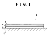
- Fig. 1 is a cross-sectional view showing an oxide superconductive element of tunnel junction type using an insulating composition of the present invention as an insulating layer, and in the drawing, the oxide superconductive element 1 is formed on the substrate 2 and is constituted by laminating Bi2Sr2Ca1Cu2O 8+ ⁇ layer 3, Bi2Sr2Y1Cu2O 8+ ⁇ layer 4 and Bi2Sr2Ca1Cu2O 8+ ⁇ layer 5 in sequence.
- Bi2O3 powder of 33.5 mol %, SrCO3 powder of 33.5 mol %, CaCO3 powder or 33.5 mol % and CuO powder or 16.7 mol % are mixed in a monopot with zirconia balls and subject to wet grinding, and after drying for removing water, a heat treatment for pre-sintering (850°C to 900°C, 24 hours) is conducted. Thereafter, a wet grinding is conducted again in a monopot, and after drying for removing water, powders (superconductor) of 5 ⁇ m or less in grain size are obtained.
- a granulation material is adjusted by adding polyvinylalcohol to the raw powders mentioned above, and a disc of 154 mm diameter and 6.5 mm thickness is formed through process steps of filling the granulation material into a metal mold and forming under 9.81 x 10⁷ Pa (1000 Kg/cm2).
- a disc represented by Bi2Sr2Y1Cu2O 8+ ⁇ and having 154 mm diameter, 6.5 mm thickness and sintering density of 98 % is obtained by the same method as the above mentioned method except replacing the CaCO3 powders mentioned above by Y2O3 powders.
- Bi2Sr2Ca1Cu2O 8+ ⁇ layer having 1.0 um thickness is formed on a SrTiO substrate of 10 x 10 x 1 mm shape while maintaining the substrate temperature at 700°C through RF magnetron sputtering method under 7 Pa pressure or mixture gas consisting or argon of 95 mol % and oxygen of 5 mol % by using Bi2Sr2Ca1Cu2O 8+ ⁇ target.
- a Bi2Sr2Ca1Cu2O 8+ ⁇ having 10 ⁇ 3um (10 ⁇ ) thickness is formed on the Bi2Sr2Ca1Cu2O 8+ ⁇ layer by using a Bi2Sr2Y1Cu2O 8+ ⁇ target.
- a Bi2Sr2Ca1Cu2O 8+ ⁇ layer having 1.0 um thickness is formed on the Bi2Sr2Y1Cu2O 8+ ⁇ layer by the same conditions as above mentioned conditions, thereby obtaining an oxide superconductive element of tunnel junction type.
- the oxide superconductive element thus constructed has the critical temperature of 77 K and was confirmed to flow the current through respective layers by tunnel effect at the temperature.
- An oxide superconductive element is formed by the same manner as mentioned above except forming a Tl2Ba2Y1Cu2O 8+ ⁇ layer as the insulating layer using a Tl2Ba2Y1Cu2O 8+ ⁇ layer Tl2Ba2Ca1Cu2O 8+ ⁇ layer as the super conductor using a Tl2Ba2Ca1Cu2O 8+ ⁇ target, and it was confirmed to operate at the critical temperature of 100 K.
- An oxide superconductive element having the same structure as Example 1 except, in place of Bi2Sr2Y1Cu2O 8+ ⁇ layer 4 in Example 1, forming an A12O3 layer of the same thickness was manufactured. However, the element did not operate at the critical temperature of 77 K.
- a monocrystalline Bi2Sr2YCu2O 8+ ⁇ of 20mm x 20mm x 2mm configuration is produced by a method including the steps of weighing raw powders or Bi2O3, SrCO3, Y2O3, CuO by a balance of 100g weighing so that the atomic ratio of Bi:Sr:Y:Cu is 3:2:1:3, mixing them, putting in an alumina crucible, keeping at 1150 °C for 24 hours under atmosphere, thereafter cooling gradually to 800°C by taking 100 hours, and cooling to room temperature.
- the specimen was confirmed to be monocrystalline and to have (001) facets by an X-ray diffraction method.
- An oxide superconductive monocrystalline film having an aligned direction with the substrate was obtained by Bi2Sr2CaCu2O 8+ ⁇ film formed on this substrate mentioned above through an RF sputter method keeping the substrate temperature at 550°C.
- the reaction between the substrate and the film was within measuring limit when the section of the film was analyzed by EPMA.
- a film was formed by the same conditions as in the Example 3 except using a MgO monocrystalline as the substrate.
- the film was of C face oriented, however, it was a polycrystalline having the orientation degree of about 70 % and having large concavities and convexities at its surface, and MgO ions were detected within the film by EPMA analysis on the film section.
- a monocrystalline of Bi2Sr2Nd2Cu3O 10+ ⁇ having 10mm x 10mm x 1mm size was forced by weighting Bi, Sr, Nd, Cu to 4:2:2:5 in the atomic ratio in this order and growing monocrystalline in the same manner as in Example 3, and it was confirmed to be monocrystalline and to have (001) facets by an X-ray diffraction method.
- Bi2Sr2Ca2Cu3O 10+ ⁇ film was formed on the substrate by a cluster ion beam method at a substrate temperature of 450°C, an oxide superconductive monocrystalline film aligning its direction with the substrate was obtained.
- the mixture was put in an alumina crucible, heated to 1150 °C under atmosphere, melted uniformly by keeping it at this temperature, thereafter cooled gradually to 800 °C by taking 100 hours during 24 hours and then cooled to room temperature.
- the large monocrystalline of 10mm x 20mm x 2mm was formed in the obtained cooled solid material.
- this monocrystalline was found to be BiPbSr2Y1Cu2O 8+ ⁇ ( ⁇ denotes oxygen defect) and of C face oriented to monocrystalline face.
- the electric resistivity was 104 ⁇ cm at -100 °C, it was found to be able to use an insulating material.
- Bi series oxide superconductor film having 2 x 10 ⁇ 2 ⁇ m (200 ⁇ ) thickness was formed through multi-sputtering method of RF magnetron sputtering under 7 Pa pressure of mixture gas consisting or argon of 95 mol % and oxygen Of 5 mol % by using Bi2O3, PbO, SrCO3, CaCO3 and CuO as sputtering target.
- the obtained Bi series oxide superconductor film was found to be an epitaxially grown film aligning its direction with the substrate.
- BiPbSr2Y1Cu2O 8+ ⁇ film having thickness 5 x 10 ⁇ 3 ⁇ m (50 ⁇ ) was formed through multi-sputtering method of RF magnetron sputtering by using Bi2O3, PbO, SrCO3, Y2O3 and CuO in the sputtering target. Thereafter, on the obtained film, Bi series oxide superconductor film having thickness 2x10 ⁇ 2 ⁇ m (200 ⁇ ) was formed in the above manner to manufacture a Josephson element.
- the element represented the superconductive characteristics at the transition temperature of 110 K and a good Josephson effect.
- a Josephson element was manufactured by using SrTiO3 as the substrate, and by laminating Bi2Sr2Ca2Cu3O 10+ ⁇ superconductor of 2 x 10 ⁇ 2 ⁇ m (200 ⁇ ), MgO of 5 x 10 ⁇ 3um (50 ⁇ ) as the insulating layer and Bi2Sr2Ca2Cu3O 10+ ⁇ superconductor of 2 x 10 ⁇ 2 ⁇ m (200 ⁇ ) in sequence on the substrate.
- Fig. 3 shows lattice constants in Bi 2-w Pb w Sr2YCu2O 8+ ⁇ crystal and Bi2Sr2CaCu2O 8+ ⁇ superconductor, and modulation structure in Bi 2-w Pb w Sr2YCu2O 8+ ⁇ crystal.
- the horizontal axis denotes W. That is, with increasing W, the ratio of replacing Bi by Pb is increased.
- the vertical axis at the left-upper side denotes lattice constant of c axis
- the vertical axis at the right-lower side denotes the lattice constants of a and b axis.
- the vertical axis at the right-upper side denotes the modulation structure.
- ⁇ signs denote lattice constant at a axis in Bi 2-w Pb w Sr2YCu2O 8+ ⁇ crystal
- ⁇ signs denote the lattice constant at b axis
- ⁇ signs denote the lattice constant at c axis.
- Insulative monocrystallines were manufactured through flux methods in accordance to compositions shown in table 1 and table 2.
- TABLE 1 Example Bi2O3 mol % SrCO3 mol % Y2O3 mol % CuO mol % cooling speed size of monocrystalline (mm3) 7 20.00 16.67 6.67 35.00 10°C/h 10 x 15 x 2 8 15.00 26.67 6.67 30.00 30°C/h 14 x 20 x 2 9 15.00 26.67 6.67 30.00 10°C/h 18 x 20 x 2 10 15.00 26.67 6.67 30.00 1°C/h 18 x 20 x 2 11 22.50 26.67 6.67 15.00 10°C/h 14 x 18 x 2 12 7.50 36.67 9.17 30.00 10°C/h 10 x 15 x 2 13 7.50 20.00 5.00 55.00 10°C/h 10 x 14 x 2 TABLE 2
Landscapes
- Chemical & Material Sciences (AREA)
- Engineering & Computer Science (AREA)
- Ceramic Engineering (AREA)
- Manufacturing & Machinery (AREA)
- Materials Engineering (AREA)
- Structural Engineering (AREA)
- Organic Chemistry (AREA)
- Inorganic Chemistry (AREA)
- Inorganic Compounds Of Heavy Metals (AREA)
- Superconductor Devices And Manufacturing Methods Thereof (AREA)
Claims (23)
- Composition isolante caractérisée en ce que Ca, dans une composition d'oxyde supraconducteur constituée de Bi, Sr, Ca, Cu et O ou de Tl, Ba, Ca, Cu et O, est remplacé par RE, alors que RE est un élément choisi dans le groupe constitué de Nd, Sm, Eu, Gd, Tb, Dy, Ho, Er, Tm, Ym, Yb, Lu et Y.
- Composition isolante selon la revendication 1, caractérisée en ce que le rapport atomique de Bi, Sr, RE, Cu et O ou de Tl, Ba, RE, Cu et O est 2 : X : Y : Z : 8+δ avec
1,5 ≦ X ≦ 2,5
0,5 ≦ Y ≦ 1,5
1,8 ≦ Z ≦ 2,5
δ = défaut d'oxygène - Procédé de formation d'une composition isolante comprenant Bi, Sr, RE, Cu et O avec pour rapport atomique
2 : X : Y : Z : 8+δ; où
1,5 ≦ X ≦ 2,5
0,5 ≦ Y ≦ 1,5
1,8 ≦ Z ≦ 2,5
δ = défaut d'oxygène
RE : un élément choisi dans le groupe constitué de Nd, Sm, Eu, Gd, Tb, Dy, Ho, Er, Tm, Ym, Yb, Lu et Y,
caractérisé en ce que l'on utilise une méthode à flux, le flux comprenant Bi₂O₃ et CuO. - Procédé de formation d'une composition isolante comprenant Bi, Sr, RE, Cu et O avec, pour rapport atomique:
2 : X : Y : Z : 8 + δ, où
1,5 ≦ X ≦ 2,5
0,5 ≦ Y ≦ 1,5
1,8 ≦ Z ≦ 2,5
δ = défaut d'oxygène
RE : un élément choisi dans le groupe constitué de Nd, Sm, Eu, Gd, Tb, Dy, Ho, Er, Tm, Ym, Yb, Lu et Y,
caractérisé en ce que les teneurs en ions positifs dans les matières premières correspondantes de Bi, Sr, RE, Cu assurent la formule suivante dans une méthode par flux:
βBi₂O₃ + γ[(Sr.RE)O] + εCuO, avec pour rapport % molaire (β, γ, ε)
conforme aux relations
5 ≦ β ≦ 25
20 ≦ γ ≦ 60
10 ≦ ε ≦ 60

- Composition isolante selon la revendication 1, caractérisée en ce qu'une partie de Bi est remplacée par Pb.
- Composition isolante selon la revendication 5, caractérisée en ce que le rapport atomique de Bi, Pb, Sr, RE, Cu, O est
2-W : W : 2 : 1 : 2 : 8+δ
avec
O < W ≦ 1,5
δ est le défaut d'oxygène - Composition isolante selon la revendication 6, caractérisée en ce que W est conforme à la relation
0,2 ≦ W ≦ 1,0 - Composition isolante selon la revendication 5, caractérisée en ce que le rapport atomique de Bi, Pb, Sr, RE, Cu, O est
2-W : W : 2 : 2 : 3 : 10+δ
avec
O < W ≦ 1,5
δ est le défaut d'oxygène - Composition isolante selon la revendication 8, caractérisée en ce que W est conforme à la relation:
0,2 ≦ W ≦ 1,0 - Elément supraconducteur caractérisé en ce que, sur un oxyde supraconducteur, on forme la composition d'oxyde isolant selon la revendication 1 qui sert de couche isolante.
- Elément supraconducteur caractérisé en ce qu'un onde supraconducteur est formé sur ladite composition isolante de la revendication 1, par application sur un substrat.
- Elément supraconducteur comprenant une couche d'oxyde isolant et une couche d'oxyde supraconducteur formée sur la couche isolante, dans lequel la couche isolante est constituée essentiellement d'un oxyde ayant une structure cristalline identique à celle de l'oxyde supraconducteur et ayant une composition caractérisée en ce que Ca, dans une composition d'oxyde supraconducteur constituée essentiellement de Bi, Sr, Ca, Cu et O ou de Tl, Ba, Ca, Cu et O est replacé par RE, alors que RE est un élément choisi dans le groupe constitué de Nd, Sm, Eu, Gd, Tb, Dy, Ho, Er, Tm, Yb, Lu et Y.
- Elément supraconducteur selon la revendication 12, dans lequel la couche isolante est un substrat.
- Elément supraconducteur selon la revendication 12, dans lequel la couche isolante forme une jonction avec la couche supraconductrice.
- Elément supraconducteur selon la revendication 12, dans lequel l'élément est un élément de Josephson.
- Elément supraconducteur selon la revendication 12, dans lequel la couche supraconductrice est une couche obtenue par croissance épitaxique sur la couche isolante.
- Elément supraconducteur selon la revendication 12, dans lequel la couche isolante présente la composition de la couche supraconductrice partiellement modifiée.
- Elément supraconducteur selon la revendication 12, dans lequel la composition de la couche isolante est caractérisee par un rapport atomique de Bi, Sr, RE, Cu et O ou de Tl, Ba, RE, Cu et O égal à
2 : X : Y : Z : 8+δ
avec
1,5 ≦ X ≦ 2,5
0,5 ≦ Y ≦ 1,5
1,8 ≦ Z ≦ 2,5
δ = défaut d'oxygène - Elément supraconducteur selon la revendication 12, la composition de la couche isolante étant caractérisée en ce qu'une partie de Bi est remplacée par Pb.
- Elément supraconducteur selon la revendication 19, dans lequel la composition de la couche isolante est caractérisée en ce que le rapport atomique de Bi, Pb, Sr, RE, Cu, O est
2-w : W : 2 : 1 : 2 : 8+δ
avec
0 < W ≦ 1,5
δ est un défaut d'oxygène. - Elément supraconducteur selon la revendication 20, dans lequel la composition de la couche isolante est caractérisée en ce que W est conforme à la relation:
0,2 ≦ W ≦ 1,0. - Elément supraconducteur selon la revendication 19, dans lequel la composition de la couche isolante est caractérisée en ce que le rapport atomique de Bi, Pb, Sr, RE, Cu, O est
2-w : W : 2 : 2 : 3 : 10-δ
avec
0 < W ≦ 1,5
δ est un défaut d'oxygène - Elément supraconducteur selon la revendication 22, dans lequel la composition de la couche isolante est caractérisée en ce que W est conforme à la relation:
0,2 ≦ W ≦ 1,0.
Applications Claiming Priority (4)
| Application Number | Priority Date | Filing Date | Title |
|---|---|---|---|
| JP8673088 | 1988-04-08 | ||
| JP86730/88 | 1988-04-08 | ||
| JP100281/88 | 1988-04-25 | ||
| JP10028188 | 1988-04-25 |
Publications (3)
| Publication Number | Publication Date |
|---|---|
| EP0337699A2 EP0337699A2 (fr) | 1989-10-18 |
| EP0337699A3 EP0337699A3 (en) | 1990-05-30 |
| EP0337699B1 true EP0337699B1 (fr) | 1994-03-16 |
Family
ID=26427821
Family Applications (1)
| Application Number | Title | Priority Date | Filing Date |
|---|---|---|---|
| EP89303514A Expired - Lifetime EP0337699B1 (fr) | 1988-04-08 | 1989-04-10 | Composition d'oxyde isolant utilisée dans un élément supraconducteur |
Country Status (3)
| Country | Link |
|---|---|
| US (2) | US5034359A (fr) |
| EP (1) | EP0337699B1 (fr) |
| DE (1) | DE68913787T2 (fr) |
Families Citing this family (8)
| Publication number | Priority date | Publication date | Assignee | Title |
|---|---|---|---|---|
| JPH01305580A (ja) * | 1988-06-03 | 1989-12-08 | Mitsubishi Metal Corp | 半導体素子製造用超電導セラミック薄膜形成単結晶ウエハー材 |
| US5306699A (en) * | 1988-08-31 | 1994-04-26 | Superconductor Technologies, Inc. | Reactor vessel for manufacture of superconducting films |
| DE69016283T3 (de) * | 1989-06-30 | 1998-04-02 | Sumitomo Electric Industries | Substrat mit einer supraleitenden Schicht. |
| JPH03259576A (ja) * | 1990-03-09 | 1991-11-19 | Sumitomo Electric Ind Ltd | ジョセフソン接合 |
| JPH04270117A (ja) * | 1991-02-26 | 1992-09-25 | Sharp Corp | 酸化物超伝導体材料 |
| US5567673A (en) * | 1994-10-17 | 1996-10-22 | E. I. Du Pont De Nemours And Company | Process of forming multilayered Tl-containing superconducting composites |
| US5985356A (en) * | 1994-10-18 | 1999-11-16 | The Regents Of The University Of California | Combinatorial synthesis of novel materials |
| US6624122B1 (en) * | 2000-06-21 | 2003-09-23 | The Regents Of The University Of California | High critical current superconducting tapes |
Family Cites Families (6)
| Publication number | Priority date | Publication date | Assignee | Title |
|---|---|---|---|---|
| EP0284061A3 (fr) * | 1987-03-24 | 1989-08-16 | Sumitomo Electric Industries Limited | Matériau composé supraconducteur en oxyde de céramique |
| JPS63250881A (ja) * | 1987-04-07 | 1988-10-18 | Semiconductor Energy Lab Co Ltd | 超電導体の作製方法 |
| US4980339A (en) * | 1987-07-29 | 1990-12-25 | Matsushita Electric Industrial Co., Ltd. | Superconductor structure |
| FR2626715B1 (fr) * | 1988-02-02 | 1990-05-18 | Thomson Csf | Dispositif en couches minces de materiau supraconducteur et procede de realisation |
| JPH01305580A (ja) * | 1988-06-03 | 1989-12-08 | Mitsubishi Metal Corp | 半導体素子製造用超電導セラミック薄膜形成単結晶ウエハー材 |
| US5047390A (en) * | 1988-10-03 | 1991-09-10 | Matsushita Electric Industrial Co., Ltd. | Josephson devices and process for manufacturing the same |
-
1989
- 1989-04-07 US US07/335,024 patent/US5034359A/en not_active Expired - Lifetime
- 1989-04-10 EP EP89303514A patent/EP0337699B1/fr not_active Expired - Lifetime
- 1989-04-10 DE DE68913787T patent/DE68913787T2/de not_active Expired - Fee Related
-
1991
- 1991-05-08 US US07/696,952 patent/US5374610A/en not_active Expired - Lifetime
Also Published As
| Publication number | Publication date |
|---|---|
| DE68913787D1 (de) | 1994-04-21 |
| EP0337699A3 (en) | 1990-05-30 |
| EP0337699A2 (fr) | 1989-10-18 |
| DE68913787T2 (de) | 1994-08-25 |
| US5034359A (en) | 1991-07-23 |
| US5374610A (en) | 1994-12-20 |
Similar Documents
| Publication | Publication Date | Title |
|---|---|---|
| EP0299879B1 (fr) | Couche mince supraconductrice et procédé de sa fabrication | |
| EP0345441B1 (fr) | Supraconducteur haute température à structure cristalline de gallate | |
| EP0299870B1 (fr) | Procédé de préparation d'une couche mince supraconductrice | |
| EP0301952A2 (fr) | Matériau supraconducteur en oxyde composé et méthode pour sa préparation | |
| US4921834A (en) | Flux method of growing oxide superconductors | |
| EP0337699B1 (fr) | Composition d'oxyde isolant utilisée dans un élément supraconducteur | |
| EP0341148B1 (fr) | Substrat semiconducteur ayant une couche mince supraconductrice | |
| EP0301958B1 (fr) | Matériau supraconducteur et procédé pour sa fabrication | |
| EP0321184B1 (fr) | Materiau en oxyde métallique | |
| US4900710A (en) | Process of depositing an alkali metal layer onto the surface of an oxide superconductor | |
| EP0513852A2 (fr) | Matériau supraconducteur (La,Sr)Cu(O,F) | |
| EP0347336B1 (fr) | Procédé pour le dépôt d'une couche mince de supraconducteur | |
| JP2975608B2 (ja) | 絶縁性組成物 | |
| EP0358545B1 (fr) | Procédé de fabrication de couches minces supraconductrices du type au thallium | |
| KR920000224B1 (ko) | 초전도물질의 제조방법 | |
| EP0323190B1 (fr) | Matériau supraconducteur à base d'oxyde métallique | |
| EP0366510B1 (fr) | Procédé pour la préparation de supraconducteur d'oxyde composé par le système Bi-Sr-Ca-Cu | |
| EP0357500A1 (fr) | Procédé pour préparer un film mince supraconducteur de type bismuth | |
| EP0323342B1 (fr) | Substrat semi-conducteur avec une couche mince supraconductrice | |
| JP2797186B2 (ja) | 超電導体層を有する半導体基板 | |
| Inamura et al. | New materials for Josephson junction devices | |
| Tai et al. | TRANSPORT AND LOW FIELD MAGNETIC PROPERTIES OF HIGH T c Bi 2 CaSr 2 Cu 2 O 8− δ AND Tl 0.8 Ca 2 Ba 2 Cu 3 O 8+ δ COMPOUNDS | |
| JPH01162384A (ja) | 酸化物超電導素子 | |
| JPH02199056A (ja) | Bi―Sr―Ca―Cu系複合酸化物超電導体 | |
| JPH01305822A (ja) | 超電導材料の製造方法 |
Legal Events
| Date | Code | Title | Description |
|---|---|---|---|
| PUAI | Public reference made under article 153(3) epc to a published international application that has entered the european phase |
Free format text: ORIGINAL CODE: 0009012 |
|
| 17P | Request for examination filed |
Effective date: 19890509 |
|
| AK | Designated contracting states |
Kind code of ref document: A2 Designated state(s): DE FR GB |
|
| PUAL | Search report despatched |
Free format text: ORIGINAL CODE: 0009013 |
|
| AK | Designated contracting states |
Kind code of ref document: A3 Designated state(s): DE FR GB |
|
| 17Q | First examination report despatched |
Effective date: 19920131 |
|
| GRAA | (expected) grant |
Free format text: ORIGINAL CODE: 0009210 |
|
| AK | Designated contracting states |
Kind code of ref document: B1 Designated state(s): DE FR GB |
|
| REF | Corresponds to: |
Ref document number: 68913787 Country of ref document: DE Date of ref document: 19940421 |
|
| ET | Fr: translation filed | ||
| PLBE | No opposition filed within time limit |
Free format text: ORIGINAL CODE: 0009261 |
|
| STAA | Information on the status of an ep patent application or granted ep patent |
Free format text: STATUS: NO OPPOSITION FILED WITHIN TIME LIMIT |
|
| 26N | No opposition filed | ||
| PGFP | Annual fee paid to national office [announced via postgrant information from national office to epo] |
Ref country code: GB Payment date: 19970401 Year of fee payment: 9 |
|
| PGFP | Annual fee paid to national office [announced via postgrant information from national office to epo] |
Ref country code: DE Payment date: 19970418 Year of fee payment: 9 |
|
| PG25 | Lapsed in a contracting state [announced via postgrant information from national office to epo] |
Ref country code: GB Free format text: LAPSE BECAUSE OF NON-PAYMENT OF DUE FEES Effective date: 19980410 |
|
| GBPC | Gb: european patent ceased through non-payment of renewal fee |
Effective date: 19980410 |
|
| PG25 | Lapsed in a contracting state [announced via postgrant information from national office to epo] |
Ref country code: DE Free format text: LAPSE BECAUSE OF NON-PAYMENT OF DUE FEES Effective date: 19990202 |
|
| REG | Reference to a national code |
Ref country code: FR Ref legal event code: D6 |
|
| PGFP | Annual fee paid to national office [announced via postgrant information from national office to epo] |
Ref country code: FR Payment date: 20070411 Year of fee payment: 19 |
|
| REG | Reference to a national code |
Ref country code: FR Ref legal event code: ST Effective date: 20081231 |
|
| PG25 | Lapsed in a contracting state [announced via postgrant information from national office to epo] |
Ref country code: FR Free format text: LAPSE BECAUSE OF NON-PAYMENT OF DUE FEES Effective date: 20080430 |