EP0338119A2 - Procédé d'identification de rubriques invalides dans une mémoire, particulièrement dans une antrémémoire et dispositif de mise en oeuvre du procédé - Google Patents
Procédé d'identification de rubriques invalides dans une mémoire, particulièrement dans une antrémémoire et dispositif de mise en oeuvre du procédé Download PDFInfo
- Publication number
- EP0338119A2 EP0338119A2 EP19880116647 EP88116647A EP0338119A2 EP 0338119 A2 EP0338119 A2 EP 0338119A2 EP 19880116647 EP19880116647 EP 19880116647 EP 88116647 A EP88116647 A EP 88116647A EP 0338119 A2 EP0338119 A2 EP 0338119A2
- Authority
- EP
- European Patent Office
- Prior art keywords
- identifier
- address
- input
- multiplexer
- entry
- Prior art date
- Legal status (The legal status is an assumption and is not a legal conclusion. Google has not performed a legal analysis and makes no representation as to the accuracy of the status listed.)
- Granted
Links
Images


Classifications
-
- G—PHYSICS
- G06—COMPUTING OR CALCULATING; COUNTING
- G06F—ELECTRIC DIGITAL DATA PROCESSING
- G06F12/00—Accessing, addressing or allocating within memory systems or architectures
- G06F12/02—Addressing or allocation; Relocation
- G06F12/08—Addressing or allocation; Relocation in hierarchically structured memory systems, e.g. virtual memory systems
- G06F12/0802—Addressing of a memory level in which the access to the desired data or data block requires associative addressing means, e.g. caches
- G06F12/0891—Addressing of a memory level in which the access to the desired data or data block requires associative addressing means, e.g. caches using clearing, invalidating or resetting means
Definitions
- the invention relates to a method for identifying invalid entries in a memory, in particular in a cache memory, according to the preamble of claim 1 and an arrangement for performing the method.
- the entries in a memory have, in addition to the memory data, additional identifiers for determining the memory data which are to be read in each case and transmitted to the requesting unit. For example, in a partially associative memory, a given keyword is compared with the identifier in the form of lock words, and if they match, the memory data associated with the corresponding lock word are read out - see e.g. "Electronic Computing Systems", 26th year, issue 4, page 168, picture 1a.
- the identifier for each individual entry in addition to the actual date consists of a partial address, this partial address being compared with the part of the respective access address of the processing unit forming the identifier. If the two address parts are identical, a HIT-MISS control generates a hit signal and the date is transmitted to the requesting processing unit, provided that it is valid.
- a validity bit is provided for each individual entry in order to mark a data entry in a memory as valid or invalid.
- a disadvantage of the validity bit for each entry is that its storage and inclusion in the backup monitoring require additional effort for a large number of entries. Because the large number of validity bits is taken into account in the unit indicating a hit / miss, problems can also arise if, in the case of a cache memory, the HIT-MISS control, which also takes the validity bit into account, is to be implemented in a separate pin-limited module.
- the present invention is therefore based on the object of providing a method which avoids the use of a separate validity bit for each entry for the invalid identification of entries in a memory.
- the method according to the invention for identifying an invalid entry uses the respectively associated field for the identifier, in which an invalid identifier is entered. Each time an entry is read, a check is carried out to determine whether the associated identifier is a non-permissible identifier that identifies the entry as invalid.
- a further development of the method according to the invention relates to a method for cache memories in a data processing system, in which the main memory can also be accessed directly bypassing the cache memory, and the direct access to data of a coherent address area is limited.
- the identifiers for the entries consist of address parts of the access address for the main memory.
- the further method uses an area address which enables direct access to the main memory as an impermissible address.
- An arrangement for carrying out the method according to the invention has a multiplexer which is provided in the control path for the entry fields in the memory which hold the identifier.
- the respective identifier and the impermissible identifier form the two input signals for the multiplexer.
- An additional comparator is connected to the data outputs for the identifier, which is charged with the non-permitted identifier and, in the case of equality, marks the selected entry as invalid.
- the multiplexer When used on cache memory, the multiplexer is preceded by an input address register for recording the respective access address. Its outputs for the address part forming the respective identifier are connected to the one data input of the multiplexer, while the non-permissible address is applied to the second data input.
- the multiplexer can be reversed by a control signal which causes an entry to be marked as invalid.
- either a predefined bit pattern can be permanently present as an illegal address or the outputs for the address part of the address forming the illegal identifier are connected, which is stored in a second input address register when the main memory is accessed directly.
- the multiplexer is part of the output multiplexer of the cache memory, the output multiplexer having the function of forwarding the access address from one of the two input address registers to the main memory.
- the output of the multiplexer part which is assigned to the address part forming the identifier, is connected to the input for the entry fields of the cache memory which contain the identifier.
- the output signal of an OR gate which acts as a changeover signal for the multiplexer part, depends on the signal for forwarding the access address from one of the two input address registers and the control signal which causes an entry to be marked as invalid.
- Another solution variant for a cache memory with a common input address register in which the respective access address is entered via an upstream input multiplexer in two different ways, one of which is reserved for normal access and the other for direct access, uses the multiplexer for Identifier as part of the input multiplexer.
- An OR gate is connected upstream of the control input of this multiplexer part, on which, in addition to the signal for transferring the direct access address to the input address register, the control signal which causes the invalidation of an entry in the cache memory also acts.
- the part of the input address register which receives the identifier can be loaded with the non-permissible identifier which is permanently present in the direct access path in order to declare an entry invalid.
- a buffer register can be used in the normal access path of the input multiplexer for the temporary storage of the access address be provided so that the remaining address part of the original access address is still available for the selection of the respective entry in the cache when the impermissible identifier is taken over, or the part of the input address register which holds the identifier can be loaded independently of its other parts.
- FIG. 1 shows an arrangement for the invalid identification of an entry in a cache memory CASP, which is connected between the processing unit of the CPU and the main memory ASP.
- the cache memory CASP is made up of several banks with the associated entry fields TAGO to. These are addressed by the partial address ADR of the access address NORMAD stored in an input address register AR via an address control device AD-ST.
- the other part of the access address is the associated ID identifier ID, which is saved for each entry in addition to the actual date in the field for the identifier. If an entry is now to be declared invalid, a non-permitted identifier is entered in the associated field for the identifier.
- the arrangement therefore has a multiplexer MUX in the control path for the entry fields, to the one data input of which the outputs for the identifier ID belonging to the access address NORMAD are connected and to the second data input of which the impermissible identifier IDINV is present.
- This impermissible identifier IDINV either consists of a permanently present predetermined bit pattern or is formed by part of the area address WCMAD which characterizes direct access from the main memory and is stored in a second input address register WCMAR.
- the selection of the invalid identifier IDINV depends on a control signal SETINV which causes the invalid identifier, by means of which the multiplexer MUX can be reversed.
- the arrangement at the data outputs for the identifier has a comparator VG which compares the associated identifier ID with the illegal identifier IDINV during a read operation and, if they match, generates the signal INVAL in the HIT-MISS controller H / M- ST marks the entry as invalid.
- the H / M-ST controller is deactivated by the DIR signal.
- an output multiplexer AMUX is provided at the interface from the cache memory CASP to the main memory ASP, at whose one data input the access address from the input address register AR and at the second data input the direct access address from the input address register WCMAR is present.
- the output multiplexer AMUX can be reversed by the signal WCMACC, which selects which of the two access addresses - NORMAD or WCMAD - are forwarded to the main memory ASP.
- the signals DIR and WCMACC can each be derived from the operation code of a microinstruction that uses data from the address area reserved for direct access only.
- the two input address registers are also used, of which the input address register AR can be written with the access address NORMAD characterizing normal access and the input address register WCMAR with the access address WCMAD characterizing direct access.
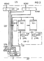
- the multiplexer MUX for the identifier ID is part of the output multiplexer AMUX arranged at the interface to the main memory ASP, the outputs for the address parts of the access addresses NORMAD and WCMAD forming the identifier ID being connected to the two data inputs of the multiplexer MUX and its output being connected to the Input for the entry fields of the cache memory which holds the identifier is connected.
- An OR gate OR is therefore connected upstream of the changeover input of this multiplexer part, on which the input signals WCMACC and SETINV act.
- the changeover signal WCMACC is used to forward the access address from one of the two input address registers AR or WCMAR to the main memory.
- the signal SETINV causes the part of the Access address WCMAD is entered as an illegal identifier in the field belonging to the corresponding entry.
- the multiplexer MUX for the identifier ID is connected upstream of the input address register AR in FIG. 3 and is a component of the input multiplexer EMUX.
- the input address register AR can be loaded via the normal access path with the access address NORMAD or via the direct access path to the main memory with the access address WCMAD.
- the OR gate OR with its two input signals WCMACC and SETINV is connected upstream in the reversing input of the multiplexer MUX.
- the signal SETINV causes the invalidation of an entry in the cache memory, as a result of which the part of the input address register AR which receives the identifier ID is loaded with the non-permissible identifier which is permanently present in the direct access path .
- a buffer register PR is therefore provided in the normal access path before the input multiplexer EMUX for the temporary storage of the normal access address NORMAD.
Landscapes
- Engineering & Computer Science (AREA)
- Theoretical Computer Science (AREA)
- Physics & Mathematics (AREA)
- General Engineering & Computer Science (AREA)
- General Physics & Mathematics (AREA)
- Memory System Of A Hierarchy Structure (AREA)
- Storage Device Security (AREA)
Applications Claiming Priority (2)
| Application Number | Priority Date | Filing Date | Title |
|---|---|---|---|
| DE3812858 | 1988-04-18 | ||
| DE3812858A DE3812858A1 (de) | 1988-04-18 | 1988-04-18 | Verfahren zur kennzeichnung ungueltiger eintraege in einem speicher, insbesondere in einem cache-speicher, und anordnung zur durchfuehrung des verfahrens |
Publications (3)
| Publication Number | Publication Date |
|---|---|
| EP0338119A2 true EP0338119A2 (fr) | 1989-10-25 |
| EP0338119A3 EP0338119A3 (en) | 1990-09-12 |
| EP0338119B1 EP0338119B1 (fr) | 1994-06-15 |
Family
ID=6352225
Family Applications (1)
| Application Number | Title | Priority Date | Filing Date |
|---|---|---|---|
| EP88116647A Expired - Lifetime EP0338119B1 (fr) | 1988-04-18 | 1988-10-07 | Procédé d'identification de rubriques invalides dans une mémoire, particulièrement dans une antrémémoire et dispositif de mise en oeuvre du procédé |
Country Status (3)
| Country | Link |
|---|---|
| EP (1) | EP0338119B1 (fr) |
| AT (1) | ATE107423T1 (fr) |
| DE (2) | DE3812858A1 (fr) |
Family Cites Families (3)
| Publication number | Priority date | Publication date | Assignee | Title |
|---|---|---|---|---|
| US4075686A (en) * | 1976-12-30 | 1978-02-21 | Honeywell Information Systems Inc. | Input/output cache system including bypass capability |
| DE3765884D1 (de) * | 1986-08-07 | 1990-12-06 | Siemens Ag | Verfahren und anordnung zum aktualisieren von steuerbitkombinationen. |
| CA1299767C (fr) * | 1987-02-18 | 1992-04-28 | Toshikatsu Mori | Systeme de commande pour antememoire |
-
1988
- 1988-04-18 DE DE3812858A patent/DE3812858A1/de not_active Withdrawn
- 1988-10-07 EP EP88116647A patent/EP0338119B1/fr not_active Expired - Lifetime
- 1988-10-07 DE DE3850243T patent/DE3850243D1/de not_active Expired - Fee Related
- 1988-10-07 AT AT88116647T patent/ATE107423T1/de not_active IP Right Cessation
Also Published As
| Publication number | Publication date |
|---|---|
| DE3812858A1 (de) | 1989-10-26 |
| ATE107423T1 (de) | 1994-07-15 |
| EP0338119A3 (en) | 1990-09-12 |
| EP0338119B1 (fr) | 1994-06-15 |
| DE3850243D1 (de) | 1994-07-21 |
Similar Documents
| Publication | Publication Date | Title |
|---|---|---|
| DE3902425C2 (fr) | ||
| DE2614000C2 (de) | Diagnoseeinrichtung zur Prüfung von Funktionseinheiten | |
| DE69031967T2 (de) | Informationsverarbeitungsanordnung | |
| DE3803759C2 (fr) | ||
| DE69031411T2 (de) | Verfahren und Anordnung zum Lesen, Schreiben und Auffrischen eines Speichers mit direktem virtuellem oder physikalischem Zugriff | |
| DE2817431C2 (de) | Speichereinrichtung mit auf Durchspeichern(store thru) beruhender Speicherhierarchie mit Teilspeicherung | |
| DE2415900A1 (de) | Rechenautomat mit mehreren mit je einem vorratsspeicher versehenen rechenanlagen | |
| EP0010186B1 (fr) | Dispositif pour traiter des pointeurs marqués | |
| DE1499182A1 (de) | Elektrische Datenverarbeitungsanlage | |
| DE2151472A1 (de) | Mikroprogrammspeicher fuer Elektronenrechner | |
| EP1113362B1 (fr) | Mémoire de semiconducteur intégrée avec une unité de mémoire pour le stockage des adresses de cellules de mémoire défectueuses | |
| DE4117672A1 (de) | Verfahren und vorrichtung zur steuerung eines zwischen einer zentraleinheit und einem arbeitsspeicher angeordneten cache-speichers | |
| DE2718551B2 (fr) | ||
| DE3586524T2 (de) | Durch beide, physikalische und virtuelle addressen, addressierbarer cache-speicher. | |
| DE3919802A1 (de) | Speicherbaustein mit vektorprozessoren und einem skalarprozessor | |
| EP1449091B1 (fr) | Procede de synchronisation d'une memoire avec la memoire principale d'un ordinateur | |
| DE4302754C1 (de) | Monolithisch integrierte Datenspeicheranordnung und Verfahren zu deren Betrieb | |
| DE2349253C3 (de) | Rechnersystem | |
| DE1574502A1 (de) | Assoziativspeicher | |
| DE3832758A1 (de) | Computerisierte arbeitsstation | |
| EP0338119B1 (fr) | Procédé d'identification de rubriques invalides dans une mémoire, particulièrement dans une antrémémoire et dispositif de mise en oeuvre du procédé | |
| DE3104941A1 (de) | Mikrorechnersystem zum raschen auffinden von kennzeichenbloecken | |
| DE4218622C2 (de) | Parallelcomputer mit Beschleunigungsfunktion | |
| DE3236524A1 (de) | Byteweise adressierbare speicheranordnung fuer befehle und daten mit variabler laenge | |
| EP0026460B1 (fr) | Dispositif de circuit pour adresser des données pour accès de lecture et d'enregistrement dans un système de traitement de données |
Legal Events
| Date | Code | Title | Description |
|---|---|---|---|
| PUAI | Public reference made under article 153(3) epc to a published international application that has entered the european phase |
Free format text: ORIGINAL CODE: 0009012 |
|
| AK | Designated contracting states |
Kind code of ref document: A2 Designated state(s): AT BE CH DE ES FR GB IT LI NL SE |
|
| PUAL | Search report despatched |
Free format text: ORIGINAL CODE: 0009013 |
|
| AK | Designated contracting states |
Kind code of ref document: A3 Designated state(s): AT BE CH DE ES FR GB IT LI NL SE |
|
| 17P | Request for examination filed |
Effective date: 19901009 |
|
| RAP1 | Party data changed (applicant data changed or rights of an application transferred) |
Owner name: SIEMENS NIXDORF INFORMATIONSSYSTEME AG |
|
| RAP3 | Party data changed (applicant data changed or rights of an application transferred) |
Owner name: SIEMENS NIXDORF INFORMATIONSSYSTEME AG |
|
| 17Q | First examination report despatched |
Effective date: 19931207 |
|
| GRAA | (expected) grant |
Free format text: ORIGINAL CODE: 0009210 |
|
| AK | Designated contracting states |
Kind code of ref document: B1 Designated state(s): AT BE CH DE ES FR GB IT LI NL SE |
|
| PG25 | Lapsed in a contracting state [announced via postgrant information from national office to epo] |
Ref country code: NL Effective date: 19940615 Ref country code: FR Effective date: 19940615 Ref country code: ES Free format text: THE PATENT HAS BEEN ANNULLED BY A DECISION OF A NATIONAL AUTHORITY Effective date: 19940615 |
|
| REF | Corresponds to: |
Ref document number: 107423 Country of ref document: AT Date of ref document: 19940715 Kind code of ref document: T |
|
| REF | Corresponds to: |
Ref document number: 3850243 Country of ref document: DE Date of ref document: 19940721 |
|
| ITF | It: translation for a ep patent filed | ||
| PG25 | Lapsed in a contracting state [announced via postgrant information from national office to epo] |
Ref country code: SE Effective date: 19940915 |
|
| PGFP | Annual fee paid to national office [announced via postgrant information from national office to epo] |
Ref country code: GB Payment date: 19940916 Year of fee payment: 7 |
|
| GBT | Gb: translation of ep patent filed (gb section 77(6)(a)/1977) |
Effective date: 19940822 |
|
| PG25 | Lapsed in a contracting state [announced via postgrant information from national office to epo] |
Ref country code: AT Effective date: 19941007 |
|
| PGFP | Annual fee paid to national office [announced via postgrant information from national office to epo] |
Ref country code: BE Payment date: 19941020 Year of fee payment: 7 |
|
| PG25 | Lapsed in a contracting state [announced via postgrant information from national office to epo] |
Ref country code: LI Effective date: 19941031 Ref country code: CH Effective date: 19941031 |
|
| EN | Fr: translation not filed | ||
| NLV1 | Nl: lapsed or annulled due to failure to fulfill the requirements of art. 29p and 29m of the patents act | ||
| PGFP | Annual fee paid to national office [announced via postgrant information from national office to epo] |
Ref country code: DE Payment date: 19941216 Year of fee payment: 7 |
|
| PLBE | No opposition filed within time limit |
Free format text: ORIGINAL CODE: 0009261 |
|
| STAA | Information on the status of an ep patent application or granted ep patent |
Free format text: STATUS: NO OPPOSITION FILED WITHIN TIME LIMIT |
|
| 26N | No opposition filed | ||
| REG | Reference to a national code |
Ref country code: CH Ref legal event code: PL |
|
| PG25 | Lapsed in a contracting state [announced via postgrant information from national office to epo] |
Ref country code: GB Effective date: 19951007 |
|
| PG25 | Lapsed in a contracting state [announced via postgrant information from national office to epo] |
Ref country code: BE Effective date: 19951031 |
|
| BERE | Be: lapsed |
Owner name: SIEMENS NIXDORF INFORMATIONSSYSTEME A.G. Effective date: 19951031 |
|
| GBPC | Gb: european patent ceased through non-payment of renewal fee |
Effective date: 19951007 |
|
| PG25 | Lapsed in a contracting state [announced via postgrant information from national office to epo] |
Ref country code: DE Effective date: 19960801 |
|
| PG25 | Lapsed in a contracting state [announced via postgrant information from national office to epo] |
Ref country code: IT Free format text: LAPSE BECAUSE OF NON-PAYMENT OF DUE FEES;WARNING: LAPSES OF ITALIAN PATENTS WITH EFFECTIVE DATE BEFORE 2007 MAY HAVE OCCURRED AT ANY TIME BEFORE 2007. THE CORRECT EFFECTIVE DATE MAY BE DIFFERENT FROM THE ONE RECORDED. Effective date: 20051007 |