EP0338158A2 - Ferro-elektrisches Festhalteverfahren - Google Patents
Ferro-elektrisches Festhalteverfahren Download PDFInfo
- Publication number
- EP0338158A2 EP0338158A2 EP88308769A EP88308769A EP0338158A2 EP 0338158 A2 EP0338158 A2 EP 0338158A2 EP 88308769 A EP88308769 A EP 88308769A EP 88308769 A EP88308769 A EP 88308769A EP 0338158 A2 EP0338158 A2 EP 0338158A2
- Authority
- EP
- European Patent Office
- Prior art keywords
- voltage
- ferroelectric
- capacitor
- ferroelectric material
- write
- Prior art date
- Legal status (The legal status is an assumption and is not a legal conclusion. Google has not performed a legal analysis and makes no representation as to the accuracy of the status listed.)
- Granted
Links
Images
Classifications
-
- G—PHYSICS
- G11—INFORMATION STORAGE
- G11C—STATIC STORES
- G11C11/00—Digital stores characterised by the use of particular electric or magnetic storage elements; Storage elements therefor
- G11C11/21—Digital stores characterised by the use of particular electric or magnetic storage elements; Storage elements therefor using electric elements
- G11C11/22—Digital stores characterised by the use of particular electric or magnetic storage elements; Storage elements therefor using electric elements using ferroelectric elements
Definitions
- This invention relates to ferroelectric materials, and particularly to a method to improve the data retention properties of such materials.
- Ferroelectric materials are dielectrics which can be used in memory circuits.
- One physical property useful in this regard relates to a hysteresis curve concerning the applied field and the polarization of the ferroelectric material.
- a capacitor can be formed having a ferroelectric material between the electrodes to serve as the dielectric. Because of the hysteresis curve, when an applied voltage is removed, the polarization of the ferroelectric material will be in one of two distinct states. These states can be determined in various fashions, typically by applying a pulse and determining the amount of current passing through the capacitor.
- Data retention refers to maintaining the physical phenomenon or property by which binary data is stored, such as ferroelectric polarization, without applied voltage. While ferroelectric materials are useful in non-volatile memory, it is desirable and important that the non-volatile memory be able to maintain the data stored therein for long periods of time, such as years. That is to say, the objective with a ferroelectric, non-volatile memory is to keep the dipoles oriented properly, without changing direction. This has been a problem in using ferroelectric materials. Consequently, an important object of this invention is to provide a way to preserve the polarization of ferroelectric materials after it has been set, without providing further power to the material, i.e. by an applied voltage.
- ferroelectric materials Another problem with ferroelectric materials relates to dipole relaxation. If the material has been in one of its two different polarization states for a relatively long time, one nevertheless wants to be able to change the polarization with a relatively short voltage pulse. For example, if a capacitor using ferroelectric material as dielectric has been in one state for a relatively long time, such as one year, and then a 100 nanosecond pulse is applied to the capacitor plates in such a direction as to change the orientation of the dipoles, then after the pulse is terminated, the dipoles may relax back to the original orientation. Problems of this nature are greater when the ferroelectric material is in a relatively thin film of below about one micron. Therefore, a further object of this invention is to provide a way to overcome the relaxation problem of ferroelectric materials.
- Ferroelectric material is used as a dielectric between two conductive plates, thus forming a ferroelectric capacitor.
- the capacitor is used to store data by using the polarization state of the ferroelectric material.
- an open circuit condition deliberately is created so that from the perspective of the ferroelectric material, a pulse of long duration is being applied.
- the ferroelectric capacitor receives its write pulse through the source-drain path of a field effect transistor (FET).
- FET field effect transistor
- the gate electrode of the FET is pulsed so that the gate closes before the drain voltage drops to zero.
- Other methods can be used to leave a charge on one plate of the capacitor so that it will dissipate mainly through the ferroelectric material.
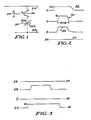
- a ferroelectric capacitor 20 has a plate 20 a coupled to a line 22, sometimes called a plate line, which is usually coupled to a reference potential, preferably ground, but which can have non-zero voltage pulses impressed thereon.
- the other capacitor plate 20 b is coupled to a second line 24, which can be called a bit line, via the source-drain path of a field effect transistor (FET) 26.
- FET field effect transistor
- Illustratively FET 26 is an N-channel device, and so the drain electrode D of FET 26 is coupled to second line 24, whereas the source electrode S of the transistor is coupled to the top electrode of capacitor 20.
- the gate electrode G is coupled to a third line 28 (sometimes called a word line) which is separately controlled. It will be understood that the present invention does not require the use of N-channel FETS. Other switching devices can be used.
- a control pulse 32 is applied on line 28 to the gate electrode G to open the gate between the drain and source.
- pulse 32 terminates prior to the trailing edge of pulse 30.
- this write voltage creates an electric field.
- the ferroelectric material polarizes in one state, and when the opposite voltage is applied, or the field is otherwise reversed, the polarization also changes.
- the polarization of the ferroelectric material in the capacitor is the mechanism by which data is stored in a non-volatile fashion. This effect is caused simply by the write voltage or pulse.
- the dipoles can be presumed initially (with no applied field) to be oriented in a random state. When a switching voltage is applied across the material, the dipoles align in one direction or the other, depending upon the direction of the voltage applied. For a high enough voltage, virtually all of the dipoles inside the ferroelectric will align in one direction. For a lower voltage, perhaps fewer than all of the dipoles will align, but the majority of them should align in one direction. In order to sense the stored information later, a logic one is defined to mean more dipoles are oriented in one direction than the other, and a logic zero is defined to mean more dipoles are oriented in the opposite direction.
- the dipoles are generally aligned in one direction corresponding to the polarity of the voltage, but when the voltage is removed, some of the dipoles normally relax back in the opposite direction. This is due to depolarization fields caused by lack of appropriate compensation charge.
- the polarization is stable only if there is an equal and opposite compensation charge inside the ferroelectric material to offset that value of polarization.
- that compensation charge moves much more slowly through the ferroelectric material than the speed with which the dipoles can be realigned by the write pulse.
- the internal compensation charge can move through the ferroelectric film to become again equal and opposite to the intended dipole polarization. Then when the write pulse ends, the ferroelectric material will be stable, with all of the dipoles aligned in the proper direction to indicate the data stored in the capacitor.
- the write pulse that is applied to the ferroelectric capacitor is very short in duration compared to the amount of time that it takes the compensation charge to move to the position where stability is achieved.
- the compensation charge is very slow-moving.
- the write pulse returns to zero volts, because the compensation charge has not moved adequately, many of those internal dipoles then want to switch back into the previous state. If more than 50% of them switch back, the data is lost.
- the reason that the compensation charge is slow-moving is twofold. First, the charge resides in the ferroelectric material, and second, the ferroelectric material typically has a high resistance. It therefore takes a long time, as mentioned, to move this compensation charge completely into that area of the ferroelectric film that needs it.
- the depolarization field caused by compensation charge in its former location does not occur.
- the effect of the open circuiting is to allow a polarizing voltage to remain across the ferroelectric material for a long enough period of time such that the resulting field inside the ferroelectric is a polarizing field, which is in a direction so that none of the dipoles want to relax back to the prior state.
- the polarizing voltage in the same direction as the write pulse, applies a polarization field which cancels or negates the depolarization field which results if the write pulse is terminated too quickly.
- the field which moves the compensation charge is also the same field that dissipates the voltage across the ferroelectric, so the rate at which the compensation charge moves is also the same rate at which the voltage dissipates. For this reason, it is preferred to create a good open circuit thereby to guarantee that the rate at which the compensation charge moves, which is essentially due to the resistance of the ferroelectric, is also the same rate at which the write voltage decays. If those rates are equal, then there can be no depolarization field built up and there can be no relaxation of dipoles.
- the resistance of the ferroelectric material is lower than the resistance on any of the other nodes around the ferroelectric.
- a junction there is a junction.
- the leakage of that junction is less than the leakage of the ferroelectric. For example, assume that 5 volts is put across the ferroelectric, and assume also that in order for this invention to work, then 5 volts needs to decay or dissipate itself mostly through the ferroelectric film itself. If there is a lower resistance path somewhere else, for example, in an MOS junction, leakage from that junction may decay the polarizing voltage quicker than the ferroelectric material would.
- the ideal situation therefore is to have a perfect open circuit so that the discharge path for those electrons would be only through the ferroelectric film itself.
- Those parallel leakage paths should be of a value that is less than that of the ferroelectric so that most of the charge is dissipated through the ferroelectric, and only a small amount of charge is dissipated through the parallel paths. If the resistance of the parallel paths is low enough, such that the voltage across the ferroelectric decayed to zero very quickly, then that in effect is just like bringing the write pulse to zero very quickly, with no open circuit.
- Figure 3 illustrates waveforms when writing the opposite state into the ferroelectric material than the Figure 2 drawings represent.
- Line 22 goes to 5 volts which is coupled to electrode 20 a of ferroelectric capacitor 20.
- Bit line 24 remains at zero volts such that the source S of FET 26 will be at zero volts. This would provide 5 volts in the opposite direction as before across the ferroelectric. One way to open circuit this logic state would be simply to turn off FET 26 prior to changing the potential of bit line 24.
- line 22 would generally be coupled to other similar lines 22. This coupling effectively precludes maintaining a given line 22 at 5 volts. So, another circuit approach can be used to return plate line 22 to zero volts and still have the logic state open circuited.
- One way in which to achieve this is to put a substrate bias on the chip, such that the source S in Fig. 1 can be driven below ground. If the bit line 24 is at zero volts and the gate G of FET 26 is also at zero volts, then the voltage at the source S can be below ground by one threshold voltage, typically one volt.
- electrode 20 b of the ferroelectric capacitor 20 will drop from zero volts to about minus one threshold voltage or about minus one volt. That voltage is still in a polarizing direction, and should be permitted to dissipate mainly through the ferroelectric material.
Landscapes
- Engineering & Computer Science (AREA)
- Computer Hardware Design (AREA)
- Dram (AREA)
- Semiconductor Memories (AREA)
- Static Random-Access Memory (AREA)
- Non-Volatile Memory (AREA)
Applications Claiming Priority (2)
| Application Number | Priority Date | Filing Date | Title |
|---|---|---|---|
| US07/184,996 US4893272A (en) | 1988-04-22 | 1988-04-22 | Ferroelectric retention method |
| US184996 | 1988-04-22 |
Publications (3)
| Publication Number | Publication Date |
|---|---|
| EP0338158A2 true EP0338158A2 (de) | 1989-10-25 |
| EP0338158A3 EP0338158A3 (en) | 1990-04-04 |
| EP0338158B1 EP0338158B1 (de) | 1994-01-12 |
Family
ID=22679122
Family Applications (1)
| Application Number | Title | Priority Date | Filing Date |
|---|---|---|---|
| EP88308769A Expired - Lifetime EP0338158B1 (de) | 1988-04-22 | 1988-09-21 | Ferro-elektrisches Festhalteverfahren |
Country Status (5)
| Country | Link |
|---|---|
| US (1) | US4893272A (de) |
| EP (1) | EP0338158B1 (de) |
| JP (1) | JP2771551B2 (de) |
| AU (1) | AU594587B2 (de) |
| DE (1) | DE3887130T2 (de) |
Cited By (4)
| Publication number | Priority date | Publication date | Assignee | Title |
|---|---|---|---|---|
| EP0469934A3 (en) * | 1990-08-03 | 1992-09-09 | Hitachi, Ltd. | Semiconductor memory device and method of operation thereof |
| US5270967A (en) * | 1991-01-16 | 1993-12-14 | National Semiconductor Corporation | Refreshing ferroelectric capacitors |
| WO1996015537A1 (en) * | 1994-11-10 | 1996-05-23 | Symetrix Corporation | Method and apparatus for reduced fatigue in ferroelectric memory elements |
| EP0706187A3 (de) * | 1994-09-22 | 1997-11-26 | Matsushita Electric Industrial Co., Ltd. | Ferroelektrischer Speicher |
Families Citing this family (51)
| Publication number | Priority date | Publication date | Assignee | Title |
|---|---|---|---|---|
| US5109357A (en) * | 1988-04-22 | 1992-04-28 | Ramtron Corporation | DRAM memory cell and method of operation thereof for transferring increased amount of charge to a bit line |
| DE3850567T2 (de) * | 1988-04-22 | 1994-11-03 | Ramtron Int Corp | DRAM-Zelle mit verstärkter Ladung. |
| US4888733A (en) * | 1988-09-12 | 1989-12-19 | Ramtron Corporation | Non-volatile memory cell and sensing method |
| JPH088339B2 (ja) * | 1988-10-19 | 1996-01-29 | 株式会社東芝 | 半導体メモリ |
| US5136534A (en) * | 1989-06-30 | 1992-08-04 | Texas Instruments Incorporated | Method and apparatus for a filament channel pass gate ferroelectric capacitor memory cell |
| US5192704A (en) * | 1989-06-30 | 1993-03-09 | Texas Instruments Incorporated | Method and apparatus for a filament channel pass gate ferroelectric capacitor memory cell |
| US5121353A (en) * | 1989-07-06 | 1992-06-09 | Kabushiki Kaisha Toshiba | Ferroelectric capacitor memory circuit MOS setting and transmission transistor |
| US5038323A (en) * | 1990-03-06 | 1991-08-06 | The United States Of America As Represented By The Secretary Of The Navy | Non-volatile memory cell with ferroelectric capacitor having logically inactive electrode |
| US5400275A (en) * | 1990-06-08 | 1995-03-21 | Kabushiki Kaisha Toshiba | Semiconductor memory device using ferroelectric capacitor and having only one sense amplifier selected |
| DE4119248A1 (de) * | 1990-06-21 | 1992-01-02 | Seiko Instr Inc | Integrierter halbleiterschaltkreis |
| US5119154A (en) * | 1990-12-03 | 1992-06-02 | Micron Technology, Inc. | Ferroelectric capacitor and method for forming local interconnect |
| US5273927A (en) * | 1990-12-03 | 1993-12-28 | Micron Technology, Inc. | Method of making a ferroelectric capacitor and forming local interconnect |
| US5309390A (en) * | 1990-12-19 | 1994-05-03 | The Charles Stark Draper Laboratory, Inc. | Ferroelectric space charge capacitor memory |
| US5262983A (en) * | 1990-12-19 | 1993-11-16 | The Charles Stark Draper Laboratories | Ferroelectric space charge capacitor analog memory |
| US5343421A (en) * | 1990-12-19 | 1994-08-30 | The Charles Stark Draper Laboratories, Inc. | Self-biased ferroelectric space charge capacitor memory |
| EP0516031A1 (de) * | 1991-05-29 | 1992-12-02 | Ramtron International Corporation | Ferroelektrische Stapelspeicherzelle und Herstellungsverfahren |
| US5142437A (en) * | 1991-06-13 | 1992-08-25 | Ramtron Corporation | Conducting electrode layers for ferroelectric capacitors in integrated circuits and method |
| US5303182A (en) * | 1991-11-08 | 1994-04-12 | Rohm Co., Ltd. | Nonvolatile semiconductor memory utilizing a ferroelectric film |
| JP3118063B2 (ja) * | 1992-03-23 | 2000-12-18 | ローム株式会社 | 不揮発性記憶素子およびこれを利用した不揮発性記憶装置、ならびに不揮発性記憶素子の製造方法 |
| US5563081A (en) * | 1992-03-23 | 1996-10-08 | Rohm Co., Inc. | Method for making a nonvolatile memory device utilizing a field effect transistor having a ferroelectric gate film |
| US5191510A (en) * | 1992-04-29 | 1993-03-02 | Ramtron International Corporation | Use of palladium as an adhesion layer and as an electrode in ferroelectric memory devices |
| US5309391A (en) * | 1992-10-02 | 1994-05-03 | National Semiconductor Corporation | Symmetrical polarization enhancement in a ferroelectric memory cell |
| US5432731A (en) * | 1993-03-08 | 1995-07-11 | Motorola, Inc. | Ferroelectric memory cell and method of sensing and writing the polarization state thereof |
| US5406510A (en) * | 1993-07-15 | 1995-04-11 | Symetrix Corporation | Non-volatile memory |
| US5608246A (en) * | 1994-02-10 | 1997-03-04 | Ramtron International Corporation | Integration of high value capacitor with ferroelectric memory |
| US5504699A (en) * | 1994-04-08 | 1996-04-02 | Goller; Stuart E. | Nonvolatile magnetic analog memory |
| US5589284A (en) * | 1994-08-01 | 1996-12-31 | Texas Instruments Incorporated | Electrodes comprising conductive perovskite-seed layers for perovskite dielectrics |
| US5554564A (en) * | 1994-08-01 | 1996-09-10 | Texas Instruments Incorporated | Pre-oxidizing high-dielectric-constant material electrodes |
| US5489548A (en) * | 1994-08-01 | 1996-02-06 | Texas Instruments Incorporated | Method of forming high-dielectric-constant material electrodes comprising sidewall spacers |
| US5622893A (en) * | 1994-08-01 | 1997-04-22 | Texas Instruments Incorporated | Method of forming conductive noble-metal-insulator-alloy barrier layer for high-dielectric-constant material electrodes |
| US5566045A (en) * | 1994-08-01 | 1996-10-15 | Texas Instruments, Inc. | High-dielectric-constant material electrodes comprising thin platinum layers |
| US5585300A (en) * | 1994-08-01 | 1996-12-17 | Texas Instruments Incorporated | Method of making conductive amorphous-nitride barrier layer for high-dielectric-constant material electrodes |
| US5504041A (en) * | 1994-08-01 | 1996-04-02 | Texas Instruments Incorporated | Conductive exotic-nitride barrier layer for high-dielectric-constant materials |
| US5541870A (en) * | 1994-10-28 | 1996-07-30 | Symetrix Corporation | Ferroelectric memory and non-volatile memory cell for same |
| US5753946A (en) * | 1995-02-22 | 1998-05-19 | Sony Corporation | Ferroelectric memory |
| US5508954A (en) * | 1995-02-27 | 1996-04-16 | Symetrix Corporation | Method and apparatus for reduced fatigue in ferroelectric memory |
| US5592410A (en) * | 1995-04-10 | 1997-01-07 | Ramtron International Corporation | Circuit and method for reducing a compensation of a ferroelectric capacitor by multiple pulsing of the plate line following a write operation |
| US5579257A (en) * | 1995-08-31 | 1996-11-26 | Motorola, Inc. | Method for reading and restoring data in a data storage element |
| US5592411A (en) * | 1995-11-02 | 1997-01-07 | Motorola, Inc. | Non-volatile register and method for accessing data therein |
| US5721699A (en) * | 1996-03-18 | 1998-02-24 | Symetrix Corporation | Ferroelectric memory with feedback circuit |
| US5724283A (en) * | 1996-06-14 | 1998-03-03 | Motorola, Inc. | Data storage element and method for restoring data |
| US6242299B1 (en) | 1999-04-01 | 2001-06-05 | Ramtron International Corporation | Barrier layer to protect a ferroelectric capacitor after contact has been made to the capacitor electrode |
| KR100308188B1 (ko) * | 1999-04-27 | 2001-10-29 | 윤종용 | 안정된 감지 마진을 가지는 강유전체 랜덤 액세스 메모리 |
| CN101101789A (zh) * | 2002-07-23 | 2008-01-09 | 松下电器产业株式会社 | 铁电门器件 |
| US20050174841A1 (en) * | 2004-02-05 | 2005-08-11 | Iota Technology, Inc. | Electronic memory with tri-level cell pair |
| US7352619B2 (en) * | 2004-02-05 | 2008-04-01 | Iota Technology, Inc. | Electronic memory with binary storage elements |
| US8723654B2 (en) | 2010-07-09 | 2014-05-13 | Cypress Semiconductor Corporation | Interrupt generation and acknowledgment for RFID |
| US9846664B2 (en) | 2010-07-09 | 2017-12-19 | Cypress Semiconductor Corporation | RFID interface and interrupt |
| US9092582B2 (en) | 2010-07-09 | 2015-07-28 | Cypress Semiconductor Corporation | Low power, low pin count interface for an RFID transponder |
| US8842460B2 (en) | 2012-11-26 | 2014-09-23 | Cypress Semiconductor Corporation | Method for improving data retention in a 2T/2C ferroelectric memory |
| US10186595B2 (en) | 2016-08-05 | 2019-01-22 | Northwestern University | Noncentrosymmetric metal electrodes for ferroic devices |
Family Cites Families (12)
| Publication number | Priority date | Publication date | Assignee | Title |
|---|---|---|---|---|
| US2938194A (en) * | 1955-07-25 | 1960-05-24 | Bell Telephone Labor Inc | Ferroelectric storage circuits |
| BE550048A (de) * | 1955-11-21 | |||
| US3132326A (en) * | 1960-03-16 | 1964-05-05 | Control Data Corp | Ferroelectric data storage system and method |
| US3354442A (en) * | 1964-03-10 | 1967-11-21 | Rca Corp | Ferroelectric switching circuits |
| US3537079A (en) * | 1967-11-29 | 1970-10-27 | Research Corp | Ferroelectric storage device |
| US3623031A (en) * | 1968-03-30 | 1971-11-23 | Hitachi Ltd | Ferroelectric storage device using gadolinium molybdate |
| US3599185A (en) * | 1968-07-10 | 1971-08-10 | Gulf & Western Industries | Ferroelectric capacitor output amplifier detector |
| US3691535A (en) * | 1970-06-15 | 1972-09-12 | Sperry Rand Corp | Solid state memory array |
| JPS51274A (de) * | 1974-06-18 | 1976-01-05 | Mitsubishi Electric Corp | |
| JPS5845114B2 (ja) * | 1975-05-26 | 1983-10-07 | 日本電気株式会社 | ハンドウタイキオクソウチ |
| US4873664A (en) * | 1987-02-12 | 1989-10-10 | Ramtron Corporation | Self restoring ferroelectric memory |
| EP0293798B2 (de) * | 1987-06-02 | 1998-12-30 | National Semiconductor Corporation | Nichtflüchtige Speicheranordnung mit einem kapazitiven ferroelektrischen Speicherelement |
-
1988
- 1988-04-22 US US07/184,996 patent/US4893272A/en not_active Expired - Lifetime
- 1988-09-21 DE DE3887130T patent/DE3887130T2/de not_active Expired - Fee Related
- 1988-09-21 EP EP88308769A patent/EP0338158B1/de not_active Expired - Lifetime
- 1988-09-29 AU AU22954/88A patent/AU594587B2/en not_active Ceased
- 1988-10-05 JP JP63250014A patent/JP2771551B2/ja not_active Expired - Fee Related
Cited By (6)
| Publication number | Priority date | Publication date | Assignee | Title |
|---|---|---|---|---|
| EP0469934A3 (en) * | 1990-08-03 | 1992-09-09 | Hitachi, Ltd. | Semiconductor memory device and method of operation thereof |
| EP1024498A3 (de) * | 1990-08-03 | 2002-05-08 | Hitachi, Ltd. | Betriebsverfahren und Anordnung eines Halbleiterspeichers |
| US5270967A (en) * | 1991-01-16 | 1993-12-14 | National Semiconductor Corporation | Refreshing ferroelectric capacitors |
| EP0706187A3 (de) * | 1994-09-22 | 1997-11-26 | Matsushita Electric Industrial Co., Ltd. | Ferroelektrischer Speicher |
| US5898608A (en) * | 1994-09-22 | 1999-04-27 | Matsushita Electric Industrial Co., Ltd. | Method for operating a ferroelectric memory |
| WO1996015537A1 (en) * | 1994-11-10 | 1996-05-23 | Symetrix Corporation | Method and apparatus for reduced fatigue in ferroelectric memory elements |
Also Published As
| Publication number | Publication date |
|---|---|
| EP0338158A3 (en) | 1990-04-04 |
| JPH01277395A (ja) | 1989-11-07 |
| AU2295488A (en) | 1989-11-30 |
| US4893272A (en) | 1990-01-09 |
| DE3887130T2 (de) | 1994-05-19 |
| AU594587B2 (en) | 1990-03-08 |
| EP0338158B1 (de) | 1994-01-12 |
| DE3887130D1 (de) | 1994-02-24 |
| JP2771551B2 (ja) | 1998-07-02 |
Similar Documents
| Publication | Publication Date | Title |
|---|---|---|
| EP0338158B1 (de) | Ferro-elektrisches Festhalteverfahren | |
| US6627944B2 (en) | Floating gate memory device using composite molecular material | |
| EP1002319B1 (de) | Ferroelektrische datenverarbeitungsanordnung | |
| US20210125656A1 (en) | Memory cell arrangement and methods thereof | |
| KR100297874B1 (ko) | 강유전체랜덤액세스메모리장치 | |
| KR102031523B1 (ko) | 메모리 셀 구성요소의 임계 전압 변동 보상 | |
| US10706906B2 (en) | Cell performance recovery using cycling techniques | |
| US10957383B2 (en) | Memory cell sensing based on precharging an access line using a sense amplifier | |
| TWI707359B (zh) | 具有分裂電容器之感測放大器 | |
| US10978126B2 (en) | Ground reference scheme for a memory cell | |
| US4685085A (en) | Non-volatile ram cell with charge pumps | |
| US5892714A (en) | Method of programming and/or verifying a threshold voltage level of a nonvolatile memory cell | |
| US20180350421A1 (en) | Boosting a digit line voltage for a write operation | |
| JP6913109B2 (ja) | メモリセルプレート間の電荷共有 | |
| WO1991006121A1 (en) | Ferro-electric non-volatile variable resistive element | |
| KR19990029298A (ko) | 전계 효과 트랜지스터 | |
| JP2021520593A (ja) | 多段階メモリセンシング | |
| US6438021B2 (en) | Methods of reading and writing data from/ on semiconductor memory device, and method for driving the device | |
| US7443710B2 (en) | Control of memory devices possessing variable resistance characteristics | |
| US20010051402A1 (en) | Ferroelectric random access memory (FRAM) device and method for controlling read/write operations thereof | |
| US20210183445A1 (en) | Charge separation for memory sensing | |
| US6421268B2 (en) | Method for driving semiconductor memory | |
| US6834006B2 (en) | Method and circuit for reading data from a ferroelectric memory cell | |
| US7283382B2 (en) | Minimization of signal loss due to self-erase of imprinted data | |
| JP2002270789A (ja) | 強誘電体メモリ |
Legal Events
| Date | Code | Title | Description |
|---|---|---|---|
| PUAI | Public reference made under article 153(3) epc to a published international application that has entered the european phase |
Free format text: ORIGINAL CODE: 0009012 |
|
| AK | Designated contracting states |
Kind code of ref document: A2 Designated state(s): DE FR GB IT NL |
|
| PUAL | Search report despatched |
Free format text: ORIGINAL CODE: 0009013 |
|
| AK | Designated contracting states |
Kind code of ref document: A3 Designated state(s): DE FR GB IT NL |
|
| 17P | Request for examination filed |
Effective date: 19900619 |
|
| 17Q | First examination report despatched |
Effective date: 19920605 |
|
| RAP1 | Party data changed (applicant data changed or rights of an application transferred) |
Owner name: RAMTRON INTERNATIONAL CORPORATION |
|
| GRAA | (expected) grant |
Free format text: ORIGINAL CODE: 0009210 |
|
| AK | Designated contracting states |
Kind code of ref document: B1 Designated state(s): DE FR GB IT NL |
|
| REF | Corresponds to: |
Ref document number: 3887130 Country of ref document: DE Date of ref document: 19940224 |
|
| ET | Fr: translation filed | ||
| ITF | It: translation for a ep patent filed | ||
| PGFP | Annual fee paid to national office [announced via postgrant information from national office to epo] |
Ref country code: NL Payment date: 19940930 Year of fee payment: 7 |
|
| PLBE | No opposition filed within time limit |
Free format text: ORIGINAL CODE: 0009261 |
|
| STAA | Information on the status of an ep patent application or granted ep patent |
Free format text: STATUS: NO OPPOSITION FILED WITHIN TIME LIMIT |
|
| PGFP | Annual fee paid to national office [announced via postgrant information from national office to epo] |
Ref country code: FR Payment date: 19941212 Year of fee payment: 7 |
|
| 26N | No opposition filed | ||
| PG25 | Lapsed in a contracting state [announced via postgrant information from national office to epo] |
Ref country code: NL Effective date: 19960401 |
|
| PG25 | Lapsed in a contracting state [announced via postgrant information from national office to epo] |
Ref country code: FR Effective date: 19960531 |
|
| NLV4 | Nl: lapsed or anulled due to non-payment of the annual fee |
Effective date: 19960401 |
|
| REG | Reference to a national code |
Ref country code: FR Ref legal event code: ST |
|
| REG | Reference to a national code |
Ref country code: GB Ref legal event code: 732E |
|
| REG | Reference to a national code |
Ref country code: GB Ref legal event code: IF02 |
|
| PGFP | Annual fee paid to national office [announced via postgrant information from national office to epo] |
Ref country code: GB Payment date: 20020918 Year of fee payment: 15 |
|
| PGFP | Annual fee paid to national office [announced via postgrant information from national office to epo] |
Ref country code: DE Payment date: 20020925 Year of fee payment: 15 |
|
| PG25 | Lapsed in a contracting state [announced via postgrant information from national office to epo] |
Ref country code: GB Free format text: LAPSE BECAUSE OF NON-PAYMENT OF DUE FEES Effective date: 20030921 |
|
| PG25 | Lapsed in a contracting state [announced via postgrant information from national office to epo] |
Ref country code: DE Free format text: LAPSE BECAUSE OF NON-PAYMENT OF DUE FEES Effective date: 20040401 |
|
| GBPC | Gb: european patent ceased through non-payment of renewal fee |
Effective date: 20030921 |
|
| PG25 | Lapsed in a contracting state [announced via postgrant information from national office to epo] |
Ref country code: IT Free format text: LAPSE BECAUSE OF NON-PAYMENT OF DUE FEES;WARNING: LAPSES OF ITALIAN PATENTS WITH EFFECTIVE DATE BEFORE 2007 MAY HAVE OCCURRED AT ANY TIME BEFORE 2007. THE CORRECT EFFECTIVE DATE MAY BE DIFFERENT FROM THE ONE RECORDED. Effective date: 20050921 |