EP0338628B1 - Système de commutation pour communications en mode circuit et/ou paquet - Google Patents
Système de commutation pour communications en mode circuit et/ou paquet Download PDFInfo
- Publication number
- EP0338628B1 EP0338628B1 EP89200957A EP89200957A EP0338628B1 EP 0338628 B1 EP0338628 B1 EP 0338628B1 EP 89200957 A EP89200957 A EP 89200957A EP 89200957 A EP89200957 A EP 89200957A EP 0338628 B1 EP0338628 B1 EP 0338628B1
- Authority
- EP
- European Patent Office
- Prior art keywords
- access unit
- time slot
- address
- output
- switch system
- Prior art date
- Legal status (The legal status is an assumption and is not a legal conclusion. Google has not performed a legal analysis and makes no representation as to the accuracy of the status listed.)
- Expired
Links
- 230000006854 communication Effects 0.000 title claims description 57
- 238000004891 communication Methods 0.000 title claims description 56
- 230000015654 memory Effects 0.000 claims description 41
- 238000001514 detection method Methods 0.000 claims description 9
- 238000012986 modification Methods 0.000 description 5
- 230000004048 modification Effects 0.000 description 5
- 238000012546 transfer Methods 0.000 description 5
- 238000000034 method Methods 0.000 description 3
- 230000008707 rearrangement Effects 0.000 description 3
- 230000005540 biological transmission Effects 0.000 description 1
- 238000010586 diagram Methods 0.000 description 1
- 230000001360 synchronised effect Effects 0.000 description 1
- 238000009827 uniform distribution Methods 0.000 description 1
- 238000012795 verification Methods 0.000 description 1
Images

Classifications
-
- H—ELECTRICITY
- H04—ELECTRIC COMMUNICATION TECHNIQUE
- H04L—TRANSMISSION OF DIGITAL INFORMATION, e.g. TELEGRAPHIC COMMUNICATION
- H04L12/00—Data switching networks
- H04L12/64—Hybrid switching systems
Definitions
- Such a switch system is known from "A Packet/Circuit Switch" by Z.L. Budrikis and A.N. Netravali in AT&T Bell Laboraties Technical Journal, Vol. 63, No. 8, October 1984, pp. 1499-1519.
- Fig. 1 The known system is diagrammatically shown in Fig. 1.
- This Figure shows two serial memories, a central controller and a number of access units.
- the subscribers are connected to the switch system via the access units.
- the serial memories are used as communication channels amongst the access units, the one serial memory functioning as forward channel and the other as backward channel.
- the consecutive access units in the switch system are connected to the read- and write points of consecutive memory locations of the serial memories, each access unit being connected to both serial memories.
- Fig. 2 showing a detail of the system as is shown in Fig. 1 in which the serial memories are arranged as shift registers whose consecutive delay stages form the memory locations.
- Dedicated to each delay stage is an OR-gate, whose first input terminal is linked with the output of the preceding delay stage, which also forms the read connection of the memory location to the dedicated access unit and whose second input terminal forms the write connection of the memory location to that access unit.
- Each access unit has an address and can reach any other access unit via one of the channels. If an access unit wishes to reach another access unit of higher address than its own address, the forward channel is used. On the other hand, if an access unit wishes to reach another access unit of lower address, the backward channel is used.
- Each slot comprises, as shown diagrammatically in Fig. 3, a number of consecutive bit sequences of which the first sequence is determined by a single slot-occupancy bit (BUSY), indicating whether the time slot is accessible or not; the second sequence by a single request bit (RQST), the third 14-bit sequence by the receiver address (RCVR); the fourth 14-bit sequence by the sender address (SNDR), the fifth 24-byte sequence by data to be transferred and, ultimately, the fifth 2-bit sequence by synchronizing bits (SYNC).
- BUSY slot-occupancy bit
- the busy bit is equal to one, which means that the slot is engaged. If an access unit is unable to find idle time slots for transferring its data packet via a channel, the unit will set the request bit in an arbitrary slot in the other channel to one.
- the operation of the system shown in Figs. 1-3 is as follows. If an access unit wants to communicate and transmit, for example, data packets to another access unit of higher address, the forward channel has to be used. The transmitting access unit will first verify the RQSR bit of every time slot in passage through the backward channel to be sure that none of the access units of higher address has a data packet available for transmission through the forward channel. Subsequently, this access unit will verify the busy bit of every time slot in passage through the forward channel until an idle time slot, with a busy bit equal to zero, is found.
- this access unit will move the busy bit to one and write the information for RCVR, SNDR and data into the idle time slot in the forward channel.
- the access unit can exchange through the second input of the associated OR-gate a series of zeroes for ones, which zeroes were offered by the associated delay stage of the shift register at bit positions determined by the access unit. If a time slot in passage through a channel is not accessible to an access unit, whereas the latter does have data packets to be transmitted, this access unit will move the RQSR bit in one of the time slots of the other channel to one.
- All access units verify the RCVR bits in every passing time slot. If the RCVR bits in a specific time slot correspond with the access unit's own address, this access unit will read out the data in this time slot. Only the access units of higher address than the address of the transmitting access unit can receive through the forward channel.
- the known switch system has a great disadvantage that with data communications the possibility of transmitting data packets is not evenly distributed over all access units.
- the access units of the switch system divide into two groups, one with low-address access units and the other with high-address access units, the latter have more chance of sending data packets through the forward channel than the low-address access units.
- the low-address access units have more chance of sending data packets through the backward channel than the high-address access units.
- the low-address access units can be blocked by the RQST bits, which are continuously transmitted by high-address access units.
- the central controller offers a time slot with zeroes at all bit positions except for the synchronizing bits and, with real-time communications the busy bit and the sender address bits, at which bit positions having zeros the access units, if so desired, can write ones.
- Fig. 1 shows a switch system for real-time and/or data communications which is known from the abovementioned article by Z.L. Budrikis et al.
- This system comprises a central controller 1 with a pair of input lines 2 and 3 and a pair of output lines 4 and 5.
- the output line 5 is connected to the input terminal 6 of a serial memory 7, whose output terminal 8 by means of input line 3 is again connected to the central controller 1.
- the output line 4 is connected to the input terminal 9 of a second serial memory 10, whose output terminal 11 by means of the input line 2 is again connected to the central controller 1.
- the respective input and output terminals 12a and 12b of access units 12 are connected to the read and write links of each memory position of both the serial memory 7 and the serial memory 10.
- each access unit 12 is linked with a memory position of serial memory 7 which is situated as many memory positions away from the input of this memory 7 as the memory position of the serial memory 10, with which the same access unit is linked, is situated away from the output of memory 10.
- Each access unit 12 is used for having a subscriber 21 communicate with the access unit 12 of a further subscriber 21 through one of the two communication channels 7 or 10.
- the subscribers may consist of telephones, computers, telefax equipment and so on.
- the entire system as shown in Fig. 1 is controlled by a clock circuit 20, enabling the whole system to operate synchronously.
- any type of memory described in the abovementioned article can be used for the serial memory, but for simplicity a shift register is preferably used having a plurality of delay stages, which is at least equal to the number of linked access units.
- Fig. 2 shows a portion of such a shift register comprising a plurality of delay stages 7′ and 10′, respectively, controlled by a clock pulse circuit 20, an access unit being connected via its input 12a to the output of each delay stage, the output 12b of each access unit always being connected to the first input terminal of an OR-gate 13, whose second input terminal is connected to the said output of the delay stage.
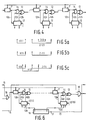
- Fig. 4 shows a first modification of the system according to the invention as shown in Figs. 1 and 2, for simplicity only the forward channel being shown because the backward channel is realized completely identical, this modification creating the option in real-time communications to use a specific time slot in a specific pattern for communication between a plurality of pairs of access units.
- a specific time slot is used for real-time communications by a plurality of pairs of access units it is necessary, after the data are read out by a receiving access unit, that at any rate the next access unit in the series to which the same time slot has been assigned by the central controller can write in this time slot at the desired bit locations at least the data in the form of zeroes and ones depending on the message to be communicated.
- the receiver address and also the data have to be written anew.
- each access unit comprises an AND-gate 14 in addition to the already available OR-gate 13. Furthermore, each access unit includes in addition to output terminal 12b connected to the first input terminal of the associated OR-gate a second output terminal 12c, which is connected to a first input terminal of the AND-gate 14. The output terminal of the associated delay stage 7′ or 10′ is connected to the second input terminal of AND-gate 14, the output terminal of the AND-gate 14 being connected to the second input terminal of the OR-gate 13. Naturally, the output terminal of the delay stage is connected as in the known system to the input terminal 12a of the access unit.
- Fig. 6 shows a second modification for the switch system as shown in Figs. 1 and 2, whilst also for data communications in the form of packet-switched traffic a considerable extension of the capacity can be achieved. Also in Fig. 6 only the forward channel is shown for clarity, because the backward channel has an identical structure. The entension of the capacity is achieved by always providing a reset line 15 for the busy bit in a group of access units and an address detection unit 16. This address detection unit has as many inputs as there are access units in a group, each of these inputs being linked with one access unit from the group.
- the reason why always one group of access units comprises an address detection unit is the fact that once an access unit has detected on the basis of the receiver address (the RCVR bits) that a certain message is meant for it, the busy bit, as clearly appears from Fig. 3, which has been put a number of bit positions in advance of the last bit of the received address in the message, has already shifted a number of access units further under control of the clock signal, this number corresponding with the said distance between the two bit positions.
- the busy bit is followed by a single request bit and by a 14-bit receiver address
- no less than 16 access units 12(1)-12(16) have to be included in a group to be able to timely reset to zero the busy bit of the time slot concerned through the reset line 15.
- the address controller comprises 16 inputs 16a-16b.
- the busy bit can be reset in an access unit situated at a distance from the addressed access unit, due to which the time slot concerned is further available for taking in a new data packet.
Landscapes
- Engineering & Computer Science (AREA)
- Computer Networks & Wireless Communication (AREA)
- Signal Processing (AREA)
- Use Of Switch Circuits For Exchanges And Methods Of Control Of Multiplex Exchanges (AREA)
- Data Exchanges In Wide-Area Networks (AREA)
- Time-Division Multiplex Systems (AREA)
Claims (7)
- Un système de commutation pour des communications en commutation de circuits et/ou de paquets, comprenant une unité de commande centrale, une source de signaux d'horloge; une paire de mémoires série et une série d'unités d'accès consécutives, chacune d'elles pouvant être reliée d'une part à un terminal d'abonné associé, et d'autre part à la borne de lecture et d'écriture d'une position de mémoire associée de la première ainsi que de la seconde mémoire série, l'entrée et la sortie des deux mémoires série étant reliées à l'unité de commande centrale et l'information qui est enregistrée aux positions de mémoire des première et seconde mémoires série pouvant être transférée respectivement de la première à la dernière unité d'accès et de la dernière à la première unité d'accès, sous la commande des signaux d'horloge, l'unité de commande centrale générant des configurations de trames consécutives ayant toujours des nombres égaux de créneaux temporels, chacun d'eux contenant un nombre prédéterminé de périodes de signai d'horloge, dans lesquels on peut écrire au moins une certaine quantité de bits d'information, et chaque unité d'accès étant conçue pour écrire de nouveaux bits dans un créneau temporel à la place de bits d'information contenant une information d'une première valeur binaire, les nouveaux bits ayant une seconde valeur binaire à des positions dans ce créneau temporel qui sont déterminées par l'unité d'accès, caractérisé en ce que pour au moins un ensemble d'unités d'accès, des moyens sont prévus pour écrire également dans un créneau temporel des bits d'information ayant la première valeur binaire.
- Un système de commutation selon la revendication 1, dans lequel chaque mémoire série comprend un registre à décalage ayant un ensemble d'étages de retard, en un nombre au moins égal au nombre de l'ensemble d'unités d'accès qui sont connectées au registre à décalage, et dans lequel une première porte logique ayant une paire de bornes d'entrée est connectée entre chaque paire d'étages de retard consécutifs, la première borne de cette porte étant reliée à la sortie de l'étage de retard précédent, et la seconde étant reliée à la borne de sortie de l'unité d'accès associée, tandis que la sortie de cette porte est reliée à l'entrée de l'étage de retard suivant, caractérisé en ce que des moyens à porte logique supplémentaires sont connectés entre chaque paire d'étages de retard et sont reliés à l'un des deux étages de retard, à la porte logique et à l'unité d'accès.
- Un système de commutation selon la revendication 2, dans lequel la première valeur binaire est un zéro logique, la seconde valeur binaire est un "1" logique et la première porte logique est une porte OU, caractérisé en ce que les moyens à porte logique consistent en une porte ET ayant une borne de sortie et une paire de bornes d'entrée, la première borne d'entrée étant connectée à la sortie de l'étage de retard précédent et la seconde étant connectée à une seconde borne de sortie de l'unité d'accès associée, tandis que la borne de sortie de la porte ET est connectée à la première borne d'entrée de la porte OU.
- Un système de commutation selon l'une au moins des revendications 1 à 3, caractérisé en ce que pour des communications en commutation de circuits, l'unité de commande centrale est conçue de façon à faire passer un bit d'état occupé dans un créneau temporel spécifique, dans un état logique qui indique que ce créneau temporel est occupé, et de façon à indiquer à la fois à l'unité d'accès émettrice et à l'unité d'accès réceptrice le numéro de série de ce créneau temporel dans une configuration.
- Un système de commutation selon l'une au moins des revendications 1-3, caractérisé en ce que pour des communications en commutation de circuits, l'unité de commande centrale est conçue de façon à faire passer un bit d'état occupé dans un créneau temporel spécifique, dans un état qui indique que ce créneau temporel est occupé, et de façon à indiquer aux unités d'accès émettrices le numéro de série de ce créneau temporel dans une configuration, et l'adresse de l'unité d'accès réceptrice et en ce que l'unité d'accès émettrice est conçue de façon à écrire cette adresse dans le créneau temporel lorsqu'il arrive.
- Un système de commutation selon la revendication 1 ou 2, caractérisé en ce qu'un certain nombre d'unités d'accès et de positions de mémoire forment toujours un groupe, et en ce que pour chaque groupe il existe une unité de détection d'adresse, une ligne de restauration et des moyens à porte logique, chaque unité d'accès dans le groupe étant reliée à une entrée associée de l'unité de détection d'adresse et étant conçue de façon à lui appliquer un signal de commande si cette unité d'accès détecte sa propre adresse dans un message qui est transmis dans un créneau temporel, la sortie de l'unité de commande d'adresse étant reliée à la ligne de restauration du groupe suivant, cette sortie étant conçue de façon à produire un signal de restauration une fois que l'une des entrées a reçu un signal de commande provenant d'une unité d'accès, et la ligne de restauration du groupe précédent et la sortie de la dernière position de mémoire étant reliée à des moyens à porte logique qui sont conçus de façon à produire un signal ayant la première valeur binaire lorsqu'un signal de restauration est présent sur la ligne de restauration.
- Un système de commutation selon les revendications 3 et 6, caractérisé en ce que les moyens à porte logique comprennent une porte logique ET et en ce que le signal de restauration a pour but de restaurer à la première valeur binaire un bit d'état occupé dans un créneau temporel.
Applications Claiming Priority (2)
| Application Number | Priority Date | Filing Date | Title |
|---|---|---|---|
| NL8801033 | 1988-04-21 | ||
| NL8801033A NL8801033A (nl) | 1988-04-21 | 1988-04-21 | Schakelstelsel voor circuit- en/of pakketgeschakelde communicatie. |
Publications (2)
| Publication Number | Publication Date |
|---|---|
| EP0338628A1 EP0338628A1 (fr) | 1989-10-25 |
| EP0338628B1 true EP0338628B1 (fr) | 1992-12-23 |
Family
ID=19852174
Family Applications (1)
| Application Number | Title | Priority Date | Filing Date |
|---|---|---|---|
| EP89200957A Expired EP0338628B1 (fr) | 1988-04-21 | 1989-04-17 | Système de commutation pour communications en mode circuit et/ou paquet |
Country Status (5)
| Country | Link |
|---|---|
| US (1) | US4953158A (fr) |
| EP (1) | EP0338628B1 (fr) |
| JP (1) | JPH0216838A (fr) |
| DE (1) | DE68903986T2 (fr) |
| NL (1) | NL8801033A (fr) |
Families Citing this family (7)
| Publication number | Priority date | Publication date | Assignee | Title |
|---|---|---|---|---|
| SE469617B (sv) * | 1991-12-16 | 1993-08-02 | Ellemtel Utvecklings Ab | Paketkopplad och kretskopplad vaeljare daer varje ansluten enhet disponerar oever aatminstone en styrtidlucka |
| US6614781B1 (en) | 1998-11-20 | 2003-09-02 | Level 3 Communications, Inc. | Voice over data telecommunications network architecture |
| US6442169B1 (en) | 1998-11-20 | 2002-08-27 | Level 3 Communications, Inc. | System and method for bypassing data from egress facilities |
| JP4006871B2 (ja) * | 1999-02-25 | 2007-11-14 | 株式会社デンソー | シリアル通信装置 |
| US7324635B2 (en) | 2000-05-04 | 2008-01-29 | Telemaze Llc | Branch calling and caller ID based call routing telephone features |
| US8559443B2 (en) | 2005-07-22 | 2013-10-15 | Marvell International Ltd. | Efficient message switching in a switching apparatus |
| US9705656B2 (en) | 2013-05-03 | 2017-07-11 | Qualcomm Incorporated | Systems and methods for peer-to-peer and AP traffic multiplexing |
Family Cites Families (8)
| Publication number | Priority date | Publication date | Assignee | Title |
|---|---|---|---|---|
| JPS589619B2 (ja) * | 1979-04-18 | 1983-02-22 | 富士通株式会社 | デ−タ通信システム |
| GB2094109A (en) * | 1981-01-30 | 1982-09-08 | Eltra Corp | A method and apparatus to serially load multibit data to a terminal of a data ring system |
| US4383315A (en) * | 1981-07-20 | 1983-05-10 | Bell Telephone Laboratories, Incorporated | Idle time slot seizure and transmission facilities for loop communication system |
| US4503533A (en) * | 1981-08-20 | 1985-03-05 | Stanford University | Local area communication network utilizing a round robin access scheme with improved channel utilization |
| US4460994A (en) * | 1981-10-05 | 1984-07-17 | At&T Bell Laboratories | Loop communication system |
| JPS62189841A (ja) * | 1986-02-17 | 1987-08-19 | Nec Corp | 回線多重ル−プネツトワ−クにおける通信方式 |
| JPS62236239A (ja) * | 1986-04-08 | 1987-10-16 | Nec Corp | 回線多重ル−プネツトワ−ク |
| EP0269803A3 (fr) * | 1986-12-05 | 1990-03-07 | ANT Nachrichtentechnik GmbH | Montage pour la commutation de canaux PCM |
-
1988
- 1988-04-21 NL NL8801033A patent/NL8801033A/nl not_active Application Discontinuation
-
1989
- 1989-04-14 US US07/338,803 patent/US4953158A/en not_active Expired - Lifetime
- 1989-04-17 EP EP89200957A patent/EP0338628B1/fr not_active Expired
- 1989-04-17 DE DE8989200957T patent/DE68903986T2/de not_active Expired - Fee Related
- 1989-04-21 JP JP1100378A patent/JPH0216838A/ja active Pending
Also Published As
| Publication number | Publication date |
|---|---|
| DE68903986T2 (de) | 1993-04-29 |
| JPH0216838A (ja) | 1990-01-19 |
| US4953158A (en) | 1990-08-28 |
| EP0338628A1 (fr) | 1989-10-25 |
| NL8801033A (nl) | 1989-11-16 |
| DE68903986D1 (de) | 1993-02-04 |
Similar Documents
| Publication | Publication Date | Title |
|---|---|---|
| US3851104A (en) | Digital communications system | |
| US3796835A (en) | Switching system for tdm data which induces an asynchronous submultiplex channel | |
| US4535450A (en) | Digital signal repeating system | |
| AU575635B2 (en) | Broadband digital transmission systems | |
| EP0133567B1 (fr) | Méthode d'appel sélectif et système de communication pour détecter les demandes de service | |
| US4460994A (en) | Loop communication system | |
| KR920010220B1 (ko) | 시분할 스위칭 시스템 및 스위치 장치의 입출력 포트간의 연결 제어 방법 | |
| JPH07111517A (ja) | 通信ノード用スイッチングシステム | |
| JPH0225319B2 (fr) | ||
| EP0017988B1 (fr) | Circuit d'interface multiplex connectant processeur à un moyen de transmission synchrone | |
| JPS58217B2 (ja) | デ−タ伝送方式 | |
| US4525837A (en) | Digital signal transmission system | |
| US4953158A (en) | Switch system for circuit and/or packet-switched communications | |
| US4821263A (en) | Method and apparatus for transmitting information via a bus system | |
| EP0240873B1 (fr) | Dispositif entrée/sortie | |
| EP0829152B1 (fr) | Systeme de transfert de donnees a bus circulaire | |
| US3859465A (en) | Data transmission system with multiple access for the connected users | |
| US4586176A (en) | Method for correction of trouble in digital signal transmission system | |
| CA1168392A (fr) | Transmission de donnees | |
| EP0059821B1 (fr) | Procédé et appareil, par exemple dans un système de distribution de données, entre autres pour éviter la distorsion dans le transfert des états des signaux | |
| US6016321A (en) | Method for transmitting digital data in a continuous data stream between two subscribers of a network with a single line between each adjacent subscriber | |
| JP2005124217A (ja) | リソース制御手段を具えたデータバスシステムおよび送信ステーション | |
| JPH01161941A (ja) | 汎用モジュール内伝送方式 | |
| JPS63302641A (ja) | 複数の端末装置の同時作動装置 | |
| JP2725713B2 (ja) | 信号伝送方法 |
Legal Events
| Date | Code | Title | Description |
|---|---|---|---|
| PUAI | Public reference made under article 153(3) epc to a published international application that has entered the european phase |
Free format text: ORIGINAL CODE: 0009012 |
|
| AK | Designated contracting states |
Kind code of ref document: A1 Designated state(s): DE FR GB NL SE |
|
| 17P | Request for examination filed |
Effective date: 19900423 |
|
| RAP1 | Party data changed (applicant data changed or rights of an application transferred) |
Owner name: APT NEDERLAND B.V. Owner name: AT&T NETWORK SYSTEMS INTERNATIONAL B.V. |
|
| RAP3 | Party data changed (applicant data changed or rights of an application transferred) |
Owner name: AT&T NETWORK SYSTEMS INTERNATIONAL B.V. Owner name: AT&T NETWORK SYSTEMS NEDERLAND B.V. |
|
| 17Q | First examination report despatched |
Effective date: 19920410 |
|
| GRAA | (expected) grant |
Free format text: ORIGINAL CODE: 0009210 |
|
| AK | Designated contracting states |
Kind code of ref document: B1 Designated state(s): DE FR GB NL SE |
|
| ET | Fr: translation filed | ||
| REF | Corresponds to: |
Ref document number: 68903986 Country of ref document: DE Date of ref document: 19930204 |
|
| PLBE | No opposition filed within time limit |
Free format text: ORIGINAL CODE: 0009261 |
|
| STAA | Information on the status of an ep patent application or granted ep patent |
Free format text: STATUS: NO OPPOSITION FILED WITHIN TIME LIMIT |
|
| 26N | No opposition filed | ||
| EAL | Se: european patent in force in sweden |
Ref document number: 89200957.2 |
|
| REG | Reference to a national code |
Ref country code: GB Ref legal event code: IF02 |
|
| PGFP | Annual fee paid to national office [announced via postgrant information from national office to epo] |
Ref country code: DE Payment date: 20020628 Year of fee payment: 14 |
|
| PG25 | Lapsed in a contracting state [announced via postgrant information from national office to epo] |
Ref country code: DE Free format text: LAPSE BECAUSE OF NON-PAYMENT OF DUE FEES Effective date: 20031101 |
|
| PGFP | Annual fee paid to national office [announced via postgrant information from national office to epo] |
Ref country code: NL Payment date: 20070403 Year of fee payment: 19 |
|
| PGFP | Annual fee paid to national office [announced via postgrant information from national office to epo] |
Ref country code: SE Payment date: 20070404 Year of fee payment: 19 |
|
| PGFP | Annual fee paid to national office [announced via postgrant information from national office to epo] |
Ref country code: GB Payment date: 20070411 Year of fee payment: 19 |
|
| PGFP | Annual fee paid to national office [announced via postgrant information from national office to epo] |
Ref country code: FR Payment date: 20070411 Year of fee payment: 19 |
|
| EUG | Se: european patent has lapsed | ||
| GBPC | Gb: european patent ceased through non-payment of renewal fee |
Effective date: 20080417 |
|
| NLV4 | Nl: lapsed or anulled due to non-payment of the annual fee |
Effective date: 20081101 |
|
| PG25 | Lapsed in a contracting state [announced via postgrant information from national office to epo] |
Ref country code: NL Free format text: LAPSE BECAUSE OF NON-PAYMENT OF DUE FEES Effective date: 20081101 |
|
| REG | Reference to a national code |
Ref country code: FR Ref legal event code: ST Effective date: 20081231 |
|
| PG25 | Lapsed in a contracting state [announced via postgrant information from national office to epo] |
Ref country code: FR Free format text: LAPSE BECAUSE OF NON-PAYMENT OF DUE FEES Effective date: 20080430 |
|
| PG25 | Lapsed in a contracting state [announced via postgrant information from national office to epo] |
Ref country code: GB Free format text: LAPSE BECAUSE OF NON-PAYMENT OF DUE FEES Effective date: 20080417 |
|
| PG25 | Lapsed in a contracting state [announced via postgrant information from national office to epo] |
Ref country code: SE Free format text: LAPSE BECAUSE OF NON-PAYMENT OF DUE FEES Effective date: 20080418 |