EP0340441A2 - Photoelektrischer Schalter - Google Patents
Photoelektrischer Schalter Download PDFInfo
- Publication number
- EP0340441A2 EP0340441A2 EP89105259A EP89105259A EP0340441A2 EP 0340441 A2 EP0340441 A2 EP 0340441A2 EP 89105259 A EP89105259 A EP 89105259A EP 89105259 A EP89105259 A EP 89105259A EP 0340441 A2 EP0340441 A2 EP 0340441A2
- Authority
- EP
- European Patent Office
- Prior art keywords
- light
- comparator
- level
- voltage
- optical axis
- Prior art date
- Legal status (The legal status is an assumption and is not a legal conclusion. Google has not performed a legal analysis and makes no representation as to the accuracy of the status listed.)
- Withdrawn
Links
Images


Classifications
-
- H—ELECTRICITY
- H03—ELECTRONIC CIRCUITRY
- H03K—PULSE TECHNIQUE
- H03K17/00—Electronic switching or gating, i.e. not by contact-making and –breaking
- H03K17/94—Electronic switching or gating, i.e. not by contact-making and –breaking characterised by the way in which the control signals are generated
- H03K17/941—Electronic switching or gating, i.e. not by contact-making and –breaking characterised by the way in which the control signals are generated using an optical detector
Definitions
- This invention relates to a photoelectric switch having a light projecting part and a light receiving part, which is intended for detection of an object according to a quantity of received light changing from a beam of projected light being intercepted thereby.
- the photoelectric switch is that for deciding whether or not an object is present at a position whereat a beam of projected light is intercepted according to whether or not a beam of projected light from a light projecting part is incident on a light receiving part. It is therefore necessary that an optical axis be adjusted so that a beam of projected light from the light projecting part will be incident correctly on the light receiving part. Then, for adjustment of the optical axis, an apparatus for deciding whether or not a beam of projected light is incident correctly on the light receiving part is required at present.
- a prior art apparatus of this kind includes that of being disclosed in Japanese Utility Model Publication No. 25185/1978.
- the apparatus comprises amplifying an electrical signal from a light receiving part which is generated from the light receiving part having received a beam of projected light from a light projecting part, thereby actuating a light emission indicator provided on the light projecting part and light receiving part.
- an operation of the light emission indicator is indicative of the beam of projected light having been incident on the light receiving part.
- the light receiving part will detect it and generate an electrical signal despite the optical axis being somewhat displaced, therefore the operation of the light emission indicator itself is still not effective in discriminating whether the optical axis is adjusted to an optimum position or is as displaced somewhat.
- the apparatus is provided with a tuning indicator tube on an amplification output end of an electrical signal generated from the light receiving part on reception of a beam of projected light, namely a light reception signal.
- a tuning indicator tube on an amplification output end of an electrical signal generated from the light receiving part on reception of a beam of projected light, namely a light reception signal.
- a problem inherent in such prior art apparatuses is that it cannot be discriminated whether an optical axis is incident correctly or is displaced to incidence, or it is difficult to discriminate an incident state of the optical axis on the light projecting part side where the adjustment is made practically.
- An object of the invention is therefore to provide a photoelectric switch wherein it can definitely be discriminated whether an optical axis is incident in best condition or is somewhat displaced to incidence, and this can be discriminated visually relatively from afar, thus facilitating an adjustment of the optical axis.
- the photoelectric switch according to the invention is intended for detection of the presence of an object according to whether or not a light from a light projecting part has reached a light receiving part, comprising a voltage controlled oscillator for generating a square wave of a frequency proportional to a light reception signal level from the light receiving part, and a comparator for deciding whether or not the light reception signal level is on a voltage set at the time of adjustment or over which is higher than a voltage set for normal operation. It further comprises a gate circuit for applying a continuous signal generated by the comparator on decision being the voltage set at the time of adjustment or over and a square wave signal generated from the voltage controlled oscillator as a driving signal for an indicating light emitting element each.
- the indicating light emitting element when the light reception signal level is higher than the voltage set at the time of adjustment which is higher than the voltage set for normal operation, the indicating light emitting element is lighted statically on the continuous signal generated from the comparator, indicating that the optical axis is incident in best condition.
- the indicating light emitting element if the light reception signal level is lower than the voltage set at the time of adjustment, the indicating light emitting element is flickered on the square wave signal of a frequency proportional to the light reception signal level which is generated from the voltage controlled oscillator, indicating that the optical axis is displaced to incidence. Then, the displacement is expressed as a flicker period.
- Fig. 1 is a block diagram representing a main part construction of a photoelectric switch given in one embodiment of the invention
- Fig. 2 is a conceptional drawing for illustrating a basic construction of a general transmissive photoelectric switch
- Fig. 3 is a circuit diagram representing a concrete construction of each part shown in Fig. 1
- Fig. 4 is a circuit diagram representing another embodiment of the invention
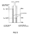
- Fig. 5 is a graph for illustrating an operation of the invention.
- a reference numeral 11 denotes a light projecting part
- 12 denotes a light receiving part
- the light projecting part 11 has a light emitting element 13 and projects a beam 15 such as infrared ray or the like toward the light receiving part 12 through an emitting lens 14.
- the light receiving part 12 has a light receiving element 16, receives the beam 15 coming from the light projecting part 11 through a receiving lens 17, and generates an electrical signal in magnitude according to a quantity of received light, namely a light reception signal.
- a reference numeral 18 denotes an object to be detected, and its presence at a predetermined position is detected by intercepting the beam 15.
- a reference numeral 21 denotes a voltage controlled oscillator, which inputs the light reception signal and generates a square wave signal of a frequency (0 Hz to 15 Hz, for example) proportional to the light reception signal level.
- a reference numeral 22 denotes a comparator, which compares the light reception signal with a set voltage Vs1 or Vs2, and generates a continuous signal of "H" level whenever the light reception signal comes to the set voltage Vs1 or Vs2 or over.
- Vs1 indicates a voltage set at the time of adjustment
- Vs2 indicates a voltage set for operation when the object is detected. Then, these voltages are set as Vs1 > Vs2.
- the set voltages Vs1, Vs2 are selected accordingly on a switch SW.
- a reference numeral 23 denotes a gate circuit, which outputs the square wave signal from the voltage controlled oscillator 21 and the continuous signal from the comparator 22 to a drive circuit 24 each, and lights up statically or flickers an indicating light emitting element (LED for example) 25.
- LED indicating light emitting element
- the voltage controlled oscillator 21 is constructed as illustrated. That is, a light reception signal Vref + V1 (Vref being a reference voltage with V1 as a variation) from the light receiving part 12 is inputted to (-) input end and (+) input end of the operational amplifier OP1 through a resistance R1 or R3.
- the (-) input end of the operational amplifier OP1 is connected to an output end of same operational amplifier OP1 through a capacitor C1, and is also connected to a supply of the reference voltage Vref through a resistance R2 and source/drain of FET Tr1. Further, (+) input end of same operational amplifier OP1 is connected to the reference voltage Vref supply through a resistance R4.
- the operational amplifier OP2 functions as a comparator, and its (-) input end is connected to the output end of the operational amplifier OP1. Then, the (+) input end is connected to a midpoint of resistances R5, R6 and also connected to an output end of same operational amplifier through a resistance R7. The output end of the operational amplifier OP2 is connected to a base of FET Tr1.
- An outgoing signal of the voltage controlled oscillator 21 is generated from the output end of the operational amplifier OP2.
- the outgoing signal is a square wave signal of a frequency proportional to a change (change of V1) of a level of the light reception signal which is an incoming signal, and changes within the range of, for example, 0 Hz to 15 Hz as mentioned hereinbefore. That is, the level of the light reception signal, or the incoming signal V1 will be maximized in best condition where an optical axis of the beam 15 from the light projecting part 11 is incident on the center of the light receiving element 16 of the light receiving part 12, therefore a frequency of the square wave signal is maximized. Then, the level V1 of the light reception signal drops according as the optical axis of the beam 15 is displaced from the center of the light receiving element 16, therefore the frequency of the square wave signal also decreases.
- the comparator 22 comprises two comparators OP3, OP4 and a changeover switch SW.
- the light reception signal Vref + V1 is impressed on each (+) input end of the comparators OP3, OP4.
- the voltage Vs1 set at the time of adjustment (Vref + 0.6V, for example) is impressed on (-) input end of the one comparator OP3.
- the voltage Vs2 set for operation (Vref + 0.25V, for example) is impressed on (-) input end of the other comparator OP4. That is, the comparator OP3 compares V1 with 0.6V for magnitude, while the comparator OP4 compares V1 with 0.25V.
- each corresponding output is inverted, and the continuous signal of "H" level is generated.
- Each output of the comparators OP3, OP4 is selected on the changeover switch SW.
- the changeover switch SW in Fig. 1 is indicated to change the set voltages Vs1, Vs2, which is different from that for changing outputs of the comparators OP3, OP4 of Fig. 3 in representation but same in content after all, and hence either will do.
- the gate circuit 23 uses an OR gate G1 inputting a square wave signal from the voltage controlled oscillator 21 and a continuous signal from the comparator OP2 or OP4 selected on the switch SW.
- An output of the OR gate G1 is fed to a base of transistor Tr2 constituting the drive circuit 24 through a resistance R9.
- the indicating light emitting element (LED for example) 25 and a resistance R10 are connected in series to a collector of the transistor Tr2 toward a power source V DD . Then, the emitter is connected to ground.
- Vs1 is selected on the switch SW in Fig. 1
- the comparator OP3 is selected on the switch SW in Fig. 3.
- the beam 15 is projected toward the light receiving part 12 from the light projecting part 11 in such state, however, if an optical axis of the beam 15 is displaced from the center of the light receiving element, the larger the displacement is, the lower the level of light reception signal Vref + V1.
- the light reception signal Vref + V1 is inputted to the voltage controlled oscillator 21 and the comparator 22.
- a square wave signal of a frequency proportional to the level (level of V1) of an incoming signal is generated from the voltage controlled oscillator 21. Accordingly, if the optical axis is displaced largely, the square wave signal of low frequency is generated.
- the comparator OP3 selected on the switch SW compares the incoming signal level V1 with the set voltage Vs1 being 0.6V for magnitude.
- the set voltage Vs1 is higher in value than the voltage set for operation at the time of normal object detection, and if the optical axis is displaced, then the incoming signal level V1 is not capable of exceeding the set voltage Vs1.
- the output of the comparator OP3 is kept on "L" level.
- the OR gate G1, or the gate circuit 23 feeds only the square wave signal from the voltage controlled oscillator 21 to a base of the transistor Tr2 of the drive circuit 24.
- the transistor Tr2 is turned on every time the square wave signal is impressed on the base, thus actuating the indicating light emitting element 25.
- the indicating light emitting element 25 thus flickers on a frequency of the square wave signal decided by the voltage controlled oscillator 21.
- the set voltage Vs1 (Vref + 0.6V) of the comparator OP3 is sufficiently high in value and is inverted to "H" level from inputting the light reception signal in best condition where the optical axis coincides with the center of the light receiving element 16.
- the "L" level is kept on until the best condition is secured. Consequently, the indicating light emitting element 25 keeps flickering until the best condition is obtained, however, the light reception signal level also rises according as the optical axis comes near to the best condition, and a frequency of the square wave signal of the voltage controlled oscillator 21 rises accordingly. That is, a flickering period of the indicating light emitting element 25 becomes short.
- the working personnel will adjust an optical axis of the beam 15 in the direction where the flickering period becomes short as observing the indicating light emitting element 25 visually. Then, when the optical axis reaches the best condition, the comparator OP3 is inverted to "H" level, and the "H" level output of the OR gate G1 is kept on, therefore the indicating light emitting element 25 is lighted up statically. Accordingly, the optical axis will be fixed finally in the state where the indicating light emitting element 25 has been lighted up statically, thus closing the adjusting work.
- Fig. 5 illustrates a relation between the aforementioned incoming signal (light reception signal) and the set voltages Vs1, Vs2 of the comparator 22, a relation between a static lighting and flickering of the indicating light emitting element, and further a flicker frequency collectively.
- a desired value for the best condition wherein the indicating light emitting element 25 is lighted statically is taken high at the time of adjustment, and the desired value is brought down somewhat at the time of detecting operation on the other hand, and thus an accurate adjustment of the optical axis is further ensured, and the system is capable of coping powerfully with a change in the environment such as oil stain, mist and the like in addition to a displacement of the optical axis.
- a mode for indicating a displacement of the optical axis is realized on the indicating light emitting element 25 in flickering which is effective in stimulating the human eyesight to observe relatively from afar, therefore the situation can be discriminated easily by far as compared with that of being hard to observe like a prior art tuning indicator tube or of changing a color of the light emitting element analogically as red ⁇ yellow ⁇ green, and the optical axis can easily be adjusted on a side of the light projecting part 11.
- the set voltages Vs1, Vs2 in the comparator 22 are changed by operating the switch SW manually, however, the system may comprise otherwise being in an adjusted state (Vs1 being selected) at the time of power closing (initialized), selecting the voltage Vs2 set for operation automatically after adjustment.
- the system may comprise otherwise being in an adjusted state (Vs1 being selected) at the time of power closing (initialized), selecting the voltage Vs2 set for operation automatically after adjustment.
- a set voltage of the comparator 22 at the time of normal object detection becomes Vs2, and a normal operation can be kept on until the incoming signal level V1 becomes 0.25V or below. Then, when V1 becomes less than 0.25V for some reason or other, the indicating light emitting element 25 recommences flickering, the switch SW is changed over to the comparator OP3, and the flickering goes on until V1 becomes greater than 0.6V.
- a beam of light is incident correctly on the light receiving part can definitely be discriminated by static lighting and flickering of the indicating light emitting element, and a displacement of the optical axis can also be discriminated by discrepancy of the flickering period, therefore the operation for adjusting the optical axis can be facilitated as compared with a prior art, and the optical axis can be optimized at high precision.
Landscapes
- Electronic Switches (AREA)
Applications Claiming Priority (2)
| Application Number | Priority Date | Filing Date | Title |
|---|---|---|---|
| JP5996688U JPH01162941U (de) | 1988-05-06 | 1988-05-06 | |
| JP59966/88 | 1988-05-06 |
Publications (2)
| Publication Number | Publication Date |
|---|---|
| EP0340441A2 true EP0340441A2 (de) | 1989-11-08 |
| EP0340441A3 EP0340441A3 (de) | 1991-01-16 |
Family
ID=13128420
Family Applications (1)
| Application Number | Title | Priority Date | Filing Date |
|---|---|---|---|
| EP19890105259 Withdrawn EP0340441A3 (de) | 1988-05-06 | 1989-03-23 | Photoelektrischer Schalter |
Country Status (2)
| Country | Link |
|---|---|
| EP (1) | EP0340441A3 (de) |
| JP (1) | JPH01162941U (de) |
Family Cites Families (5)
| Publication number | Priority date | Publication date | Assignee | Title |
|---|---|---|---|---|
| JPS515965B2 (de) * | 1972-01-28 | 1976-02-24 | ||
| JPS49113176A (de) * | 1973-03-05 | 1974-10-29 | ||
| DE3034695A1 (de) * | 1980-09-15 | 1982-04-29 | Licentia Patent-Verwaltungs-Gmbh, 6000 Frankfurt | Lichtschranke |
| DE3323214C1 (de) * | 1983-06-28 | 1984-10-11 | Dürkoppwerke GmbH, 4800 Bielefeld | Optoelektronische Abtastvorrichtung an einer Naehmaschine |
| US4595848A (en) * | 1983-06-30 | 1986-06-17 | Eaton Corporation | Adjustable frequency on/off delay circuit |
-
1988
- 1988-05-06 JP JP5996688U patent/JPH01162941U/ja active Pending
-
1989
- 1989-03-23 EP EP19890105259 patent/EP0340441A3/de not_active Withdrawn
Also Published As
| Publication number | Publication date |
|---|---|
| EP0340441A3 (de) | 1991-01-16 |
| JPH01162941U (de) | 1989-11-14 |
Similar Documents
| Publication | Publication Date | Title |
|---|---|---|
| US11412139B2 (en) | Traffic monitoring device capable of switching camera mode | |
| US4236101A (en) | Light control system | |
| DE60002832T2 (de) | Mit einem erleuchteten zielpunkt versehenes optisches visier | |
| US4595946A (en) | White balance control system including a fluorescent light ripple detector | |
| US5157435A (en) | Automatic focusing apparatus for a video camera and the method thereof | |
| US6498570B2 (en) | Optical highway line detector | |
| US4771431A (en) | Semiconductor laser drive | |
| US5623249A (en) | Video monitor motion sensor | |
| DK0418989T3 (da) | Lysspærre | |
| US4571047A (en) | TTL Focus detecting device for single-lens reflex camera | |
| US4300826A (en) | Focus indicating device for camera | |
| US4320946A (en) | Camera focus detecting device | |
| US5003378A (en) | Automatic white balance circuit | |
| US4687919A (en) | A lighting control device in manuscript reproduction equipment | |
| US4940889A (en) | Method and apparatus for visual indication of optical alignment of photoelectric switch | |
| US6094143A (en) | Light obstruction type smoke sensor | |
| US5010394A (en) | Automatic white balance circuit capable of effectively adjusting white balance under a flashing light source | |
| JP2634317B2 (ja) | 照明変化補償装置 | |
| US5821528A (en) | Two light intensities difference convert into frequency modulator for parallel photodiodes | |
| US4659939A (en) | Optical scanning system including an amplifier | |
| US4293207A (en) | Camera focus detecting device | |
| JPS6156490B2 (de) | ||
| EP0353259A4 (de) | Detektor für bewegung. | |
| US6396060B1 (en) | System for detecting radiation in the presence of more intense background radiation | |
| RU2017064C1 (ru) | Оптико-электронное устройство для измерения размеров нагретых изделий |
Legal Events
| Date | Code | Title | Description |
|---|---|---|---|
| PUAI | Public reference made under article 153(3) epc to a published international application that has entered the european phase |
Free format text: ORIGINAL CODE: 0009012 |
|
| AK | Designated contracting states |
Kind code of ref document: A2 Designated state(s): AT BE CH DE ES FR GB IT LI NL SE |
|
| PUAL | Search report despatched |
Free format text: ORIGINAL CODE: 0009013 |
|
| AK | Designated contracting states |
Kind code of ref document: A3 Designated state(s): AT BE CH DE ES FR GB IT LI NL SE |
|
| 17P | Request for examination filed |
Effective date: 19910703 |
|
| STAA | Information on the status of an ep patent application or granted ep patent |
Free format text: STATUS: THE APPLICATION IS DEEMED TO BE WITHDRAWN |
|
| 18D | Application deemed to be withdrawn |
Effective date: 19920929 |