EP0340448A2 - Procédé pour la fabrication d'une plaque de fond avec incrustation obtenue par gravure pour tête pour imprimante par jet d'encre - Google Patents
Procédé pour la fabrication d'une plaque de fond avec incrustation obtenue par gravure pour tête pour imprimante par jet d'encre Download PDFInfo
- Publication number
- EP0340448A2 EP0340448A2 EP89105396A EP89105396A EP0340448A2 EP 0340448 A2 EP0340448 A2 EP 0340448A2 EP 89105396 A EP89105396 A EP 89105396A EP 89105396 A EP89105396 A EP 89105396A EP 0340448 A2 EP0340448 A2 EP 0340448A2
- Authority
- EP
- European Patent Office
- Prior art keywords
- base plate
- ink
- nozzle outlet
- glass material
- glass
- Prior art date
- Legal status (The legal status is an assumption and is not a legal conclusion. Google has not performed a legal analysis and makes no representation as to the accuracy of the status listed.)
- Withdrawn
Links
Images

Classifications
-
- C—CHEMISTRY; METALLURGY
- C03—GLASS; MINERAL OR SLAG WOOL
- C03C—CHEMICAL COMPOSITION OF GLASSES, GLAZES OR VITREOUS ENAMELS; SURFACE TREATMENT OF GLASS; SURFACE TREATMENT OF FIBRES OR FILAMENTS MADE FROM GLASS, MINERALS OR SLAGS; JOINING GLASS TO GLASS OR OTHER MATERIALS
- C03C4/00—Compositions for glass with special properties
- C03C4/04—Compositions for glass with special properties for photosensitive glass
-
- C—CHEMISTRY; METALLURGY
- C03—GLASS; MINERAL OR SLAG WOOL
- C03C—CHEMICAL COMPOSITION OF GLASSES, GLAZES OR VITREOUS ENAMELS; SURFACE TREATMENT OF GLASS; SURFACE TREATMENT OF FIBRES OR FILAMENTS MADE FROM GLASS, MINERALS OR SLAGS; JOINING GLASS TO GLASS OR OTHER MATERIALS
- C03C15/00—Surface treatment of glass, not in the form of fibres or filaments, by etching
-
- G—PHYSICS
- G03—PHOTOGRAPHY; CINEMATOGRAPHY; ANALOGOUS TECHNIQUES USING WAVES OTHER THAN OPTICAL WAVES; ELECTROGRAPHY; HOLOGRAPHY
- G03F—PHOTOMECHANICAL PRODUCTION OF TEXTURED OR PATTERNED SURFACES, e.g. FOR PRINTING, FOR PROCESSING OF SEMICONDUCTOR DEVICES; MATERIALS THEREFOR; ORIGINALS THEREFOR; APPARATUS SPECIALLY ADAPTED THEREFOR
- G03F7/00—Photomechanical, e.g. photolithographic, production of textured or patterned surfaces, e.g. printing surfaces; Materials therefor, e.g. comprising photoresists; Apparatus specially adapted therefor
- G03F7/004—Photosensitive materials
- G03F7/0042—Photosensitive materials with inorganic or organometallic light-sensitive compounds not otherwise provided for, e.g. inorganic resists
-
- G—PHYSICS
- G03—PHOTOGRAPHY; CINEMATOGRAPHY; ANALOGOUS TECHNIQUES USING WAVES OTHER THAN OPTICAL WAVES; ELECTROGRAPHY; HOLOGRAPHY
- G03F—PHOTOMECHANICAL PRODUCTION OF TEXTURED OR PATTERNED SURFACES, e.g. FOR PRINTING, FOR PROCESSING OF SEMICONDUCTOR DEVICES; MATERIALS THEREFOR; ORIGINALS THEREFOR; APPARATUS SPECIALLY ADAPTED THEREFOR
- G03F7/00—Photomechanical, e.g. photolithographic, production of textured or patterned surfaces, e.g. printing surfaces; Materials therefor, e.g. comprising photoresists; Apparatus specially adapted therefor
- G03F7/20—Exposure; Apparatus therefor
- G03F7/2022—Multi-step exposure, e.g. hybrid; backside exposure; blanket exposure, e.g. for image reversal; edge exposure, e.g. for edge bead removal; corrective exposure
- G03F7/2032—Simultaneous exposure of the front side and the backside
Definitions
- the invention relates to a method for producing a base plate with etchings for an ink print head in ink printing units of the type specified in the preamble of claim 1.
- An inkjet printhead for use in inkjet printing units generally includes a simple ejection opening for ink, an ink channel and a portion for generating the energy for ink ejection, which is provided in a part of the ink channel.
- a method for producing such an ink print head a method was previously known in which, for example, a z. B. plate made of glass or metal is used and in this plate by a machining measure z. B. cutting or machining processing or etching a fine groove is formed and the plate is then connected to the groove with a suitable other plate, thereby forming an ink channel.
- German patent specification 27 58 142 discloses a method for producing a charging plate which is provided for charging ink droplets produced in inkjet printers and which consists of a plurality of plate-shaped layers. Since these plates are made of a photosensitive, heat-melting material, the through holes serving as ink channels can be easily etched. After the individual plates have been produced, they must be connected to one another using a suitable method. For this purpose, it is necessary that the through holes present in the individual plates are aligned with one another, which requires appropriate care and is therefore costly. This method is too complicated and expensive, particularly in the case of ink print heads with ink outlet openings arranged in several rows.
- This object is advantageously achieved by the invention characterized in claim 1.
- the ink channels, ink chambers and nozzle outlet openings for e.g. B. the nozzle outlet openings in two rows of ink printheads are located on opposite sides of a single base plate and are etched at the same time in an etching process, the adjustment required in two separate plates incorporated adjustments is not necessary.
- the method according to the invention ensures a uniform depth of all nozzle outlet openings, so that uniform ink droplets can always be produced.
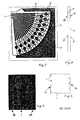
- FIG. 1 shows a base plate 1 made of a photosensitive glass material, in the surfaces 2, 3 of which ink storage chambers 4, ink pressure chambers 5, ink channels 6 and nozzle outlet openings 7 are to be etched.
- a substrate material can be used as the photosensitive glass, such as is sold under the trade name Foto-Ceram by the American company Corning Glass Works or Foturan-Glas by the German company Schott Glaswerke.
- a quartz glass plate 8, 9 is arranged on each side of the base plate 1, each of which has a mask 12, 13 applied by chromium vapor deposition on its surfaces 10, 11 facing away from the base plate 1. These masks have the ink print head layout shown in FIG. 1.
- the two chromium-vapor-coated quartz glass masks 12, 13 are mirror-symmetrical and are arranged offset to one another such that the nozzle outlet openings 7 to be formed in one row 14 are arranged centrally to the nozzle outlet openings 7 in the other row 15, see FIGS. 3 and 4.
- the base plate 1 is exposed through the two chrome-vaporized quartz glass masks 12, 13 to light of the wavelength emitted by two light sources 16, 17, for which the quartz glass material of the base plate 1 is photosensitive.
- the two light sources 16, 17 preferably supply collimated light and consist of mercury-xenon lamps.
- the openings in the masks 12, 13 correspond to the final sizes of the openings or the recesses in the base plate 1.
- nucleation points within the glass material are developed, at which crystal growth later occurs.
- the base plate is heat-treated by heating to a temperature at which the amorphous glass structure in the exposed areas is converted into a ceramic crystal structure.
- the crystalline substance that forms in the exposed areas is known as "photo opal".
- the glass is brought to its own critical temperature and held at this temperature until the crystallization process has ended.
- the manufacturer of the photo ceram glass specifies 592 ° Celsius and 30 minutes conversion time.
- the next step of the method involves immersing the base plate 1 in a suitable etching solution, from which the crystalline photo opal glass is attacked much more strongly than the photo form glass.
- the unexposed glass is called photo-shaped glass.
- a suitable etching solution is a 12% solution of hydrofluoric acid in water.
- the depth of the depressions etched into the surfaces 2, 3 of the base plate 1 depends on the time of the etching.
- a base plate 1 is shown in FIG. 2 after the etching process.
- the amount of light emitted by the light sources 16, 17 is selected so that the light does not pass through the base plate 1. This avoids that the etching can only ever take place from the exposed surfaces.
- the base plates 1 are still ground and polished. Then a membrane plate 18, 19 is arranged on the surfaces 2, 3 of the base plate 1. This attachment of the membrane plates 18, 19 to the base plate 1 can be done by gluing or by a sintering process.
- FIG. 5 shows a micrograph through the nozzle area of an ink print head, the nozzle outlet openings 7 being recognizable in front of the dark areas which contain the crystalline form.
- the dark streaks run out with increasing depth.
- the light stripes in FIG. 5 relate to the unexposed areas in the base plate 1 which are difficult to etch.
- the chromium-vaporized quartz glass masks used for exposure are mirror-symmetrical and are clamped in a mask frame in such a way that they can be adjusted relative to one another.
- the nozzle offset can be set to less than ⁇ 001 mm. All ink print heads that receive base plates 1 exposed in this way have this slight halftone error. There is no production-related variation.
- the horizontal grid spacing is determined by the etching depth and the grinding size of the base plate 1.
Landscapes
- Chemical & Material Sciences (AREA)
- Organic Chemistry (AREA)
- Life Sciences & Earth Sciences (AREA)
- Engineering & Computer Science (AREA)
- Chemical Kinetics & Catalysis (AREA)
- General Chemical & Material Sciences (AREA)
- Geochemistry & Mineralogy (AREA)
- Materials Engineering (AREA)
- Physics & Mathematics (AREA)
- General Physics & Mathematics (AREA)
- Particle Formation And Scattering Control In Inkjet Printers (AREA)
- Surface Treatment Of Glass (AREA)
Applications Claiming Priority (2)
| Application Number | Priority Date | Filing Date | Title |
|---|---|---|---|
| DE3814720 | 1988-04-30 | ||
| DE3814720A DE3814720A1 (de) | 1988-04-30 | 1988-04-30 | Verfahren zur herstellung einer grundplatte mit durch aetzen hergestellte einarbeitungen fuer einen tintendruckkopf |
Publications (2)
| Publication Number | Publication Date |
|---|---|
| EP0340448A2 true EP0340448A2 (fr) | 1989-11-08 |
| EP0340448A3 EP0340448A3 (fr) | 1991-09-11 |
Family
ID=6353307
Family Applications (1)
| Application Number | Title | Priority Date | Filing Date |
|---|---|---|---|
| EP19890105396 Withdrawn EP0340448A3 (fr) | 1988-04-30 | 1989-03-23 | Procédé pour la fabrication d'une plaque de fond avec incrustation obtenue par gravure pour tête pour imprimante par jet d'encre |
Country Status (4)
| Country | Link |
|---|---|
| US (1) | US5028514A (fr) |
| EP (1) | EP0340448A3 (fr) |
| JP (1) | JPH02204051A (fr) |
| DE (1) | DE3814720A1 (fr) |
Cited By (1)
| Publication number | Priority date | Publication date | Assignee | Title |
|---|---|---|---|---|
| EP2727880B1 (fr) | 2012-11-05 | 2016-06-08 | GFD Gesellschaft für Diamantprodukte mbH | Composant micromécanique tridimensionnel chanfreiné pour mouvement d'horlogerie et son procédé de fabrication |
Families Citing this family (18)
| Publication number | Priority date | Publication date | Assignee | Title |
|---|---|---|---|---|
| DE4033294A1 (de) * | 1990-10-19 | 1992-04-23 | Siemens Ag | Verfahren zur fotolithographischen herstellung von strukturen auf einem traeger |
| US5374291A (en) * | 1991-12-10 | 1994-12-20 | Director-General Of Agency Of Industrial Science And Technology | Method of processing photosensitive glass |
| DE4141869B4 (de) * | 1991-12-18 | 2005-11-10 | Director General Of Agency Of Industrial Science And Technology | Verfahren zur Bearbeitung von lichtempfindlichem Glas |
| JPH05169666A (ja) * | 1991-12-25 | 1993-07-09 | Rohm Co Ltd | インクジェットプリントヘッドの製造方法 |
| DE4225799A1 (de) * | 1992-07-31 | 1994-02-03 | Francotyp Postalia Gmbh | Tintenstrahldruckkopf und Verfahren zu seiner Herstellung |
| US5825382A (en) * | 1992-07-31 | 1998-10-20 | Francotyp-Postalia Ag & Co. | Edge-shooter ink jet print head and method for its manufacture |
| DE4336416A1 (de) * | 1993-10-19 | 1995-08-24 | Francotyp Postalia Gmbh | Face-Shooter-Tintenstrahldruckkopf und Verfahren zu seiner Herstellung |
| DE9404328U1 (de) * | 1994-03-10 | 1994-05-19 | Francotyp-Postalia Gmbh, 13409 Berlin | Tintenstrahldruckkopf |
| AUPN522295A0 (en) * | 1995-09-06 | 1995-09-28 | Eastman Kodak Company | Cmos process compatible fabrication of lift print heads |
| US5901425A (en) | 1996-08-27 | 1999-05-11 | Topaz Technologies Inc. | Inkjet print head apparatus |
| JP3141840B2 (ja) * | 1998-04-02 | 2001-03-07 | 日本電気株式会社 | インクジェットプリントヘッドの製造方法 |
| JP3327246B2 (ja) * | 1999-03-25 | 2002-09-24 | 富士ゼロックス株式会社 | インクジェット記録ヘッド及びその製造方法 |
| US7448734B2 (en) | 2004-01-21 | 2008-11-11 | Silverbrook Research Pty Ltd | Inkjet printer cartridge with pagewidth printhead |
| US20050157112A1 (en) | 2004-01-21 | 2005-07-21 | Silverbrook Research Pty Ltd | Inkjet printer cradle with shaped recess for receiving a printer cartridge |
| USD646238S1 (en) * | 2010-05-26 | 2011-10-04 | Ace Technologies Corp. | Strip pattern substrate for a filtering device |
| WO2014028022A1 (fr) * | 2012-08-16 | 2014-02-20 | Hewlett-Packard Development Company, L.P. | Ouvertures diagonales dans du verre photodéfinissable |
| EP3455074B1 (fr) * | 2016-10-24 | 2021-06-16 | Hewlett-Packard Development Company, L.P. | Dépôt d'un agent d'impression |
| WO2018194675A1 (fr) | 2017-04-21 | 2018-10-25 | Hewlett-Packard Development Company, L.P. | Impression dans des zones délimitées |
Family Cites Families (5)
| Publication number | Priority date | Publication date | Assignee | Title |
|---|---|---|---|---|
| FR2166560A5 (fr) * | 1971-12-30 | 1973-08-17 | Pasquet Rene | |
| US4092166A (en) * | 1976-12-27 | 1978-05-30 | International Business Machines Corporation | Double exposure and double etch technique for producing precision parts from crystallizable photosensitive glass |
| US4096626A (en) * | 1976-12-27 | 1978-06-27 | International Business Machines Corporation | Method of making multi-layer photosensitive glass ceramic charge plate |
| US4216483A (en) * | 1977-11-16 | 1980-08-05 | Silonics, Inc. | Linear array ink jet assembly |
| JPS582240A (ja) * | 1981-06-26 | 1983-01-07 | Hoya Corp | 化学切削性感光ガラスの露光方法 |
-
1988
- 1988-04-30 DE DE3814720A patent/DE3814720A1/de not_active Withdrawn
-
1989
- 1989-03-23 EP EP19890105396 patent/EP0340448A3/fr not_active Withdrawn
- 1989-04-24 JP JP1101856A patent/JPH02204051A/ja active Pending
- 1989-05-01 US US07/345,656 patent/US5028514A/en not_active Expired - Fee Related
Cited By (1)
| Publication number | Priority date | Publication date | Assignee | Title |
|---|---|---|---|---|
| EP2727880B1 (fr) | 2012-11-05 | 2016-06-08 | GFD Gesellschaft für Diamantprodukte mbH | Composant micromécanique tridimensionnel chanfreiné pour mouvement d'horlogerie et son procédé de fabrication |
Also Published As
| Publication number | Publication date |
|---|---|
| DE3814720A1 (de) | 1989-11-09 |
| US5028514A (en) | 1991-07-02 |
| JPH02204051A (ja) | 1990-08-14 |
| EP0340448A3 (fr) | 1991-09-11 |
Similar Documents
| Publication | Publication Date | Title |
|---|---|---|
| EP0340448A2 (fr) | Procédé pour la fabrication d'une plaque de fond avec incrustation obtenue par gravure pour tête pour imprimante par jet d'encre | |
| EP0726152B1 (fr) | Procédé de fabrication d'une tête d'impression à jet d'encre | |
| DE69203464T2 (de) | Akustische Tintendruckköpfe. | |
| DE2604939C3 (de) | Verfahren zum Herstellen von wenigstens einem Durchgangsloch insbesondere einer Düse für Tintenstrahldrucker | |
| DE69326204T2 (de) | Farbstrahlkopf und sein Herstellungsverfahren | |
| DE69320327T2 (de) | Maskenmuster für die Herstellung von konische Tintenstrahldüsen | |
| DE60038400T2 (de) | Laserverfahren zur Bearbeitung von Löchern nur in einer keramischen Grünfolie mit einem Trägerfilm | |
| DE2554085C3 (de) | Verfahren zur Herstellung eines Spritzkopfes für einen Tintenstrahldrucker | |
| DE69231773T2 (de) | Verfahren zum Herstellen eines Tintenstrahlaufzeichnungskopfes | |
| DE3326781C2 (fr) | ||
| DE60119998T2 (de) | Tintenstrahlaufzeichnungskopf, Verfahren zur Herstellung und Tintenstrahlaufzeichnungsgerät | |
| DE69636021T2 (de) | Tintenstrahldruckkopf und Verfahren zu seiner Herstellung | |
| DE3414792C2 (fr) | ||
| DE69907841T2 (de) | Akustisches Tintendruckverfahren und System zur Verbesserung der Uniformität durch Manipulieren nichtlinearer Merkmalen in dem System | |
| DE2752378C2 (fr) | ||
| DE102012101432A1 (de) | Verfahren zur Einstellung mindestens eines Druckkopfes in einer Druckkopfanordnung bei einem Tintendruckgerät | |
| DE60113408T2 (de) | Verfahren zur herstellung eines monolithischen druckkopfes mit verkürzten kegelförmigen düsen | |
| EP0671270B1 (fr) | Tête d'impression par jet d'encre | |
| DE3507112A1 (de) | Tintenstrahlaufzeichnungskopf | |
| DE60127642T2 (de) | Vorrichtung zum Bilden einer Düse in einem Element eines Tintenstrahldruckkopfes, Düsenelement, mit solchem Düsenelement versehener Tintenstrahldruckkopf und mit solchem Druckkopf versehener Tintenstrahldrucker | |
| DE68919768T2 (de) | Verfahren zum Herstellen einer Düsenplatte für einen Tintenstrahldruckkopf. | |
| DE69020021T2 (de) | Tintendruckkopf-Substrat und Tintendruckkopf mit einem solchen Substrat. | |
| EP0179452A2 (fr) | Procédé de fabrication de têtes d'impression pour mécanisme d'impression à encre | |
| DE69927211T2 (de) | Zeilendruckkopf für Tintenstrahldrucker | |
| WO1988010475A1 (fr) | Procede de marquage de surfaces de semi-conducteurs |
Legal Events
| Date | Code | Title | Description |
|---|---|---|---|
| PUAI | Public reference made under article 153(3) epc to a published international application that has entered the european phase |
Free format text: ORIGINAL CODE: 0009012 |
|
| AK | Designated contracting states |
Kind code of ref document: A2 Designated state(s): DE FR GB IT |
|
| RAP1 | Party data changed (applicant data changed or rights of an application transferred) |
Owner name: AEG OLYMPIA OFFICE GMBH |
|
| PUAL | Search report despatched |
Free format text: ORIGINAL CODE: 0009013 |
|
| AK | Designated contracting states |
Kind code of ref document: A3 Designated state(s): DE FR GB IT |
|
| 17P | Request for examination filed |
Effective date: 19911011 |
|
| 17Q | First examination report despatched |
Effective date: 19930208 |
|
| STAA | Information on the status of an ep patent application or granted ep patent |
Free format text: STATUS: THE APPLICATION HAS BEEN WITHDRAWN |
|
| 18W | Application withdrawn |
Withdrawal date: 19930609 |