EP0344067B1 - Linearisierungsverfahren für Gleichspannungswandler und Durchführung des Verfahrens - Google Patents
Linearisierungsverfahren für Gleichspannungswandler und Durchführung des Verfahrens Download PDFInfo
- Publication number
- EP0344067B1 EP0344067B1 EP19890401417 EP89401417A EP0344067B1 EP 0344067 B1 EP0344067 B1 EP 0344067B1 EP 19890401417 EP19890401417 EP 19890401417 EP 89401417 A EP89401417 A EP 89401417A EP 0344067 B1 EP0344067 B1 EP 0344067B1
- Authority
- EP
- European Patent Office
- Prior art keywords
- converter
- capacitor
- voltage
- current
- stage
- Prior art date
- Legal status (The legal status is an assumption and is not a legal conclusion. Google has not performed a legal analysis and makes no representation as to the accuracy of the status listed.)
- Expired - Lifetime
Links
- 238000000034 method Methods 0.000 title claims description 28
- 230000008569 process Effects 0.000 title description 12
- 239000003990 capacitor Substances 0.000 claims description 76
- 238000004804 winding Methods 0.000 claims description 64
- 230000010355 oscillation Effects 0.000 claims description 24
- 238000001514 detection method Methods 0.000 claims 1
- 238000010586 diagram Methods 0.000 description 21
- 230000002457 bidirectional effect Effects 0.000 description 19
- 208000028659 discharge Diseases 0.000 description 19
- 230000000903 blocking effect Effects 0.000 description 10
- 230000009466 transformation Effects 0.000 description 10
- 101150005287 EPS1 gene Proteins 0.000 description 8
- 230000007423 decrease Effects 0.000 description 6
- 230000008901 benefit Effects 0.000 description 4
- 230000000694 effects Effects 0.000 description 4
- 238000009499 grossing Methods 0.000 description 4
- 230000004913 activation Effects 0.000 description 3
- 230000005347 demagnetization Effects 0.000 description 3
- 230000010287 polarization Effects 0.000 description 3
- 230000009471 action Effects 0.000 description 2
- 239000000969 carrier Substances 0.000 description 2
- 230000006378 damage Effects 0.000 description 2
- 238000012423 maintenance Methods 0.000 description 2
- 238000004519 manufacturing process Methods 0.000 description 2
- 230000009467 reduction Effects 0.000 description 2
- 241001415961 Gaviidae Species 0.000 description 1
- 238000010521 absorption reaction Methods 0.000 description 1
- 238000004458 analytical method Methods 0.000 description 1
- 238000010719 annulation reaction Methods 0.000 description 1
- 230000002238 attenuated effect Effects 0.000 description 1
- 238000004364 calculation method Methods 0.000 description 1
- 230000001143 conditioned effect Effects 0.000 description 1
- 239000000470 constituent Substances 0.000 description 1
- 238000013016 damping Methods 0.000 description 1
- 230000001419 dependent effect Effects 0.000 description 1
- 238000011161 development Methods 0.000 description 1
- 230000018109 developmental process Effects 0.000 description 1
- 230000008030 elimination Effects 0.000 description 1
- 238000003379 elimination reaction Methods 0.000 description 1
- 238000005516 engineering process Methods 0.000 description 1
- 230000002349 favourable effect Effects 0.000 description 1
- 238000001914 filtration Methods 0.000 description 1
- 238000002955 isolation Methods 0.000 description 1
- 230000014759 maintenance of location Effects 0.000 description 1
- 210000000056 organ Anatomy 0.000 description 1
- 230000002093 peripheral effect Effects 0.000 description 1
- 230000010349 pulsation Effects 0.000 description 1
- 230000000630 rising effect Effects 0.000 description 1
- 238000007493 shaping process Methods 0.000 description 1
- 230000001629 suppression Effects 0.000 description 1
Images


Classifications
-
- H—ELECTRICITY
- H02—GENERATION; CONVERSION OR DISTRIBUTION OF ELECTRIC POWER
- H02M—APPARATUS FOR CONVERSION BETWEEN AC AND AC, BETWEEN AC AND DC, OR BETWEEN DC AND DC, AND FOR USE WITH MAINS OR SIMILAR POWER SUPPLY SYSTEMS; CONVERSION OF DC OR AC INPUT POWER INTO SURGE OUTPUT POWER; CONTROL OR REGULATION THEREOF
- H02M3/00—Conversion of DC power input into DC power output
- H02M3/22—Conversion of DC power input into DC power output with intermediate conversion into AC
- H02M3/24—Conversion of DC power input into DC power output with intermediate conversion into AC by static converters
- H02M3/28—Conversion of DC power input into DC power output with intermediate conversion into AC by static converters using discharge tubes with control electrode or semiconductor devices with control electrode to produce the intermediate AC
- H02M3/325—Conversion of DC power input into DC power output with intermediate conversion into AC by static converters using discharge tubes with control electrode or semiconductor devices with control electrode to produce the intermediate AC using devices of a triode or a transistor type requiring continuous application of a control signal
- H02M3/335—Conversion of DC power input into DC power output with intermediate conversion into AC by static converters using discharge tubes with control electrode or semiconductor devices with control electrode to produce the intermediate AC using devices of a triode or a transistor type requiring continuous application of a control signal using semiconductor devices only
- H02M3/33569—Conversion of DC power input into DC power output with intermediate conversion into AC by static converters using discharge tubes with control electrode or semiconductor devices with control electrode to produce the intermediate AC using devices of a triode or a transistor type requiring continuous application of a control signal using semiconductor devices only having several active switching elements
- H02M3/33576—Conversion of DC power input into DC power output with intermediate conversion into AC by static converters using discharge tubes with control electrode or semiconductor devices with control electrode to produce the intermediate AC using devices of a triode or a transistor type requiring continuous application of a control signal using semiconductor devices only having several active switching elements having at least one active switching element at the secondary side of an isolation transformer
- H02M3/33584—Bidirectional converters
-
- H—ELECTRICITY
- H02—GENERATION; CONVERSION OR DISTRIBUTION OF ELECTRIC POWER
- H02M—APPARATUS FOR CONVERSION BETWEEN AC AND AC, BETWEEN AC AND DC, OR BETWEEN DC AND DC, AND FOR USE WITH MAINS OR SIMILAR POWER SUPPLY SYSTEMS; CONVERSION OF DC OR AC INPUT POWER INTO SURGE OUTPUT POWER; CONTROL OR REGULATION THEREOF
- H02M3/00—Conversion of DC power input into DC power output
- H02M3/22—Conversion of DC power input into DC power output with intermediate conversion into AC
- H02M3/24—Conversion of DC power input into DC power output with intermediate conversion into AC by static converters
- H02M3/28—Conversion of DC power input into DC power output with intermediate conversion into AC by static converters using discharge tubes with control electrode or semiconductor devices with control electrode to produce the intermediate AC
- H02M3/325—Conversion of DC power input into DC power output with intermediate conversion into AC by static converters using discharge tubes with control electrode or semiconductor devices with control electrode to produce the intermediate AC using devices of a triode or a transistor type requiring continuous application of a control signal
- H02M3/335—Conversion of DC power input into DC power output with intermediate conversion into AC by static converters using discharge tubes with control electrode or semiconductor devices with control electrode to produce the intermediate AC using devices of a triode or a transistor type requiring continuous application of a control signal using semiconductor devices only
- H02M3/33538—Conversion of DC power input into DC power output with intermediate conversion into AC by static converters using discharge tubes with control electrode or semiconductor devices with control electrode to produce the intermediate AC using devices of a triode or a transistor type requiring continuous application of a control signal using semiconductor devices only of the forward type
- H02M3/33546—Conversion of DC power input into DC power output with intermediate conversion into AC by static converters using discharge tubes with control electrode or semiconductor devices with control electrode to produce the intermediate AC using devices of a triode or a transistor type requiring continuous application of a control signal using semiconductor devices only of the forward type with automatic control of the output voltage or current
-
- H—ELECTRICITY
- H02—GENERATION; CONVERSION OR DISTRIBUTION OF ELECTRIC POWER
- H02M—APPARATUS FOR CONVERSION BETWEEN AC AND AC, BETWEEN AC AND DC, OR BETWEEN DC AND DC, AND FOR USE WITH MAINS OR SIMILAR POWER SUPPLY SYSTEMS; CONVERSION OF DC OR AC INPUT POWER INTO SURGE OUTPUT POWER; CONTROL OR REGULATION THEREOF
- H02M3/00—Conversion of DC power input into DC power output
- H02M3/22—Conversion of DC power input into DC power output with intermediate conversion into AC
- H02M3/24—Conversion of DC power input into DC power output with intermediate conversion into AC by static converters
- H02M3/28—Conversion of DC power input into DC power output with intermediate conversion into AC by static converters using discharge tubes with control electrode or semiconductor devices with control electrode to produce the intermediate AC
- H02M3/325—Conversion of DC power input into DC power output with intermediate conversion into AC by static converters using discharge tubes with control electrode or semiconductor devices with control electrode to produce the intermediate AC using devices of a triode or a transistor type requiring continuous application of a control signal
- H02M3/335—Conversion of DC power input into DC power output with intermediate conversion into AC by static converters using discharge tubes with control electrode or semiconductor devices with control electrode to produce the intermediate AC using devices of a triode or a transistor type requiring continuous application of a control signal using semiconductor devices only
- H02M3/337—Conversion of DC power input into DC power output with intermediate conversion into AC by static converters using discharge tubes with control electrode or semiconductor devices with control electrode to produce the intermediate AC using devices of a triode or a transistor type requiring continuous application of a control signal using semiconductor devices only in push-pull configuration
- H02M3/3376—Conversion of DC power input into DC power output with intermediate conversion into AC by static converters using discharge tubes with control electrode or semiconductor devices with control electrode to produce the intermediate AC using devices of a triode or a transistor type requiring continuous application of a control signal using semiconductor devices only in push-pull configuration with automatic control of output voltage or current
Definitions
- the present invention relates to a process for linearizing the output characteristics (voltage, current) of a direct transfer pseudo-resonant DC-DC converter.
- the invention also relates to devices allowing the implementation of the method.
- a direct transfer pseudoresonant DC-DC converter comprising a transformer comprising a primary winding connected to a primary stage and a secondary winding, said secondary winding being connected to a secondary stage comprising an oscillation capacitor, a component with unidirectional conductivity connected in parallel on said capacitor and a unit with unidirectional conductivity in series with said secondary winding and said capacitor.
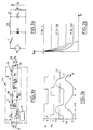
- Such an AC converter comprises a primary stage P connected to a DC voltage source E and comprising a unidirectional switching component T1 controlled by a control circuit CC.
- This primary stage P supplies the primary winding of the transformer T with transformation ratio m.
- the secondary winding of the transformer T is connected to a secondary stage S comprising a diode D2 and a capacitor C in series with the secondary winding and a diode D4 mounted in parallel on said capacitor so that the cathodes of the diodes D2 and D4 are electrically connected.
- the secondary stage S is connected to a load Ch through a filter constituted by a smoothing inductor LS and a capacitor CS intended to ensure the smoothing of the current IS and the filtering of the output voltage.
- the transformer T necessarily has a leakage inductance, brought back to the secondary on the diagram in FIG. 1a, which constitutes with the capacitor C an oscillating circuit (L, C).
- the transistor T1 of the primary stage is blocked and it is the diode D4 of the secondary stage which ensures the continuity of the current IS in the load Ch.
- the control circuit CC controls the transistor T1 in the on state, the currents I1 and I2 then increase, the diode D2 having become conductive, while the voltage Vc at the terminals of the capacitor C is maintained zero by conduction of the diode D4.
- the inductance of the transformer leakage L limits this growth.
- the current I2 has become at the instant T4 lower than the output current IS, which implies that the current IC in the capacitor C reverses and becomes negative.
- This converter processes the energy coming from a DC voltage source E to deliver a DC current IS to a load Ch.
- the energy transfer is direct because it takes place when the transistor T1 of the primary stage P is on, as opposed to other known principles where the energy transfer via the transformer takes place when the transistor T1 is in the blocked state (such as "Flyback" type mountings).
- Anglo-Saxon literature and those skilled in the art generally use the term "forward converter".
- This converter is said to be "pseudo-resonant" because the effective resonance of the circuit (L, C) is never really implemented completely because it would inevitably lead to a reverse transfer of energy from the secondary to the primary, which of course is not wanted and should be avoided.
- Diode D2 avoids the phenomenon of total resonance.
- This phenomenon corresponds to a rise in the characteristics (VS, IS) of the converter, which results in a non-proportionality of VS with respect to the adjustment parameter.
- the non-linearity of the characteristics is a major drawback when it comes to performing a control loop of the output voltage VS and more generally of inserting this converter into a controlled system.
- the non-linearity involves the implementation of very complex transfer functions which are difficult to handle in a servo calculation.
- the object of the present invention is to remedy these drawbacks by implementing a process for linearizing the output characteristics (current voltage) of a direct transfer pseudo-resonant DC-DC converter comprising a transformer comprising a primary winding, a secondary winding, an oscillation capacitor, and subjected to predetermined control cycles each comprising a direct conduction phase.
- the total discharge of the capacitor no longer depends only on the existence of a continuous output current IS, unlike what happens in the converters of the prior art in which this discharge depends exclusively on the presence of 'an output current IS.
- the division into two stages is effective in practice because, during the direct conduction phase, the capacitor C is in principle connected to the secondary winding of the transformer and that its discharge is intimately linked to the electrical state of the oscillating circuit (L, C), while at the end of this direct conduction phase, the capacitor is no longer in a resonance situation with the transformer leakage inductance.
- the step of keeping the voltage across the oscillation capacitor at a substantially zero value is preferably divided into two sub-steps, one corresponding to an active hold, allowing the reversal of the current in LS , and using holding means for a predetermined period, and the other, called safety, immediately following the first and taking place until the start of the next control cycle, during which said holding means are no longer put in action.
- This last step is made necessary in order to avoid, at the start of a new cycle, inadvertent short-circuiting of the secondary winding of the transformer.
- the voltage developed at the transformer secondary causes the diode D2 to go into the on state. This conduction combined with the effective maintenance of a substantially zero value at the terminals of the capacitor would in fact lead to a short circuit of the transformer.
- the method according to the invention can advantageously be implemented in a direct-continuous pseudo-resonant converter with direct energy transfer comprising transformers each comprising a primary winding connected to a primary stage and secondary windings, arranged in series or in parallel and with interleaved control, each of said secondary windings being connected to a secondary stage comprising an oscillation capacitor, a conductive component unidirectional connected in parallel on said capacitor and a unidirectionally conductive component in series with said secondary winding and said capacitor.
- the bidirectional current switching component produced around the conductive component unidirectional (preferably a diode) connected in series with the capacitor and one of the secondary windings of the converter according to the invention is implemented in the step of total discharge of the capacitor, while the other switching component bidirectional current is implemented in the step of maintaining at a substantially zero value of the voltage across said capacitor.
- the process for linearizing the output characteristics (voltage - current) implements a step of total discharge ED and a holding step EM, the place of which within a control period is illustrated on the timing diagram of FIG. 3, with reference to the general block diagram of converter of FIG. 4.
- a direct conduction phase CD during which the voltage applied to the winding primary EP of the transformer TR is equal to the direct voltage E, to the voltage drops in the primary stage P near.
- the ED discharge step is initiated as soon as the current in the oscillation capacitor reverses.
- the discharge step ED begins during the direct conduction phase CD. It ends with the cancellation of the voltage VC across the terminals of the capacitor C.
- the step of total discharge ED is immediately followed by a step of maintaining EM at a substantially zero value of the retention Vc at the terminals of the capacitor C.
- This step of maintaining EM is itself divided into a first step EME during which holding means are effectively implemented and in a second stage ES, called safety, during which said means are deactivated, made necessary to avoid inadvertent simultaneous conduction of several switching members during the implementation of the phase of next direct conduction, as will be explained in more detail below.
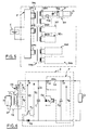
- FIG. 4 The general structure of a direct transfer pseudo-resonant DC-DC converter according to the invention comprising a transformer comprising a primary winding and a secondary winding is presented in FIG. 4, this converter implementing the method according to the invention.
- Such a converter comprises a transformer TR, a primary stage P and a secondary stage S.
- the primary stage P supplies the primary winding EP of the transformer TR from the DC voltage source E.
- the secondary stage S ensures the control of the energy from the DC voltage source E and passing through the transformer TR and its shaping to deliver to the output of a filter F a DC voltage V of adjustable value across a load arbitrary Ch. It includes a capacitor C which enters into resonance with the leakage inductance L of the transformer TR brought back to the secondary and two switching components TD2 and TD4 bidirectional in current. These two switching components are each made up of a combination of a one-way conductive component D2, D4 and a one-way switching current component T2, T4.
- a DC-DC converter 1 can comprise several transformers TR1, ..., TRN connected via a primary stage P to a single DC voltage source E, as illustrated in FIG. 5
- Each of these transformers TR1, ..., TRN can be provided with several secondary windings ES11, ... ES1M ..., ESN1, ..., ESNM each connected to a secondary stage of the type described in the figure former. These stages are arranged in series or in parallel and controlled in interlaced mode.
- the transformer TR has a transformation ratio m.
- the voltage U2 present at the terminals of the winding ES of the transformer TR is the sum of the voltage V2 (equal to the product of the transformation ratio m by the voltage V1 at the terminals of the primary) and the induced voltage VL linked to the transformer leaks represented by the leakage inductance L brought back to the secondary.
- the filter F here consists of a cell LS, CS comprising an inductance LS and a capacitor CS according to a well known embodiment.
- ILS and IS be the currents crossing respectively the inductance LS and the load Ch connected to the output terminals of the secondary stage S.
- the primary stage P is here an asymmetrical half-bridge which comprises two unidirectional switching components in current TH, TB, for example transistors, at the terminals which are connected two components with unidirectional conductivity DH, DB, for example diodes and two other components with unidirectional conductivity DD, DC, for example diodes, all of these components being connected according to a connection method well known in the art. prior art.
- the respective pairs (TH, DH) and (TB, DB) provide bidirectional current switching components. They operate simultaneously and control the supply of the primary winding EP of the transformer TR, in relation to the oscillating circuit (L, C).
- the diodes DD and DC ensure the demagnetization cycle of the magnetic circuit of the transformer TR by the primary winding EP.
- Figures 8a, 8b, 8c, 8d illustrate the main waveforms encountered in discontinuous mode in the secondary stage S of a converter according to the invention, as described above.
- the primary stage P (FIG. 7) applies to the primary winding EP a voltage V1 substantially equal to the direct supply voltage E (at the voltage drop in the switching members of the 'primary stage P near).
- the diode D2 is conducting and the capacitor C then constitutes with the leakage inductance brought back to the secondary L an oscillating circuit which enters into resonance with a non-zero damping due to the resistance of the secondary winding and of the various connections. , and to the equivalent series resistances of capacitor C and diode D2.
- the current I2 in the secondary winding will first of all increase, pass through a maximum, then decrease and finally cancel out (figure 8c), while the voltage VC across the terminals of capacitor C will reach its maximum VC1, with reference in Figure 8a.
- the unidirectional switching component of the bidirectional current switching component TD2 in this case the transistor T2 must have been controlled in passing mode, thus allowing the current I2 to take a negative value, thus ensuring the second part of the direct conduction phase CD during which the voltage VC across the terminals of the capacitor C decreases.
- This second part is also the first stage of discharge ED1 of the capacitor C which ends at the end of the direct conduction phase (CD) controlled by means of control of the primary stage P.
- the instant of phase end direct conduction (CD) is predetermined as a function of the pulsation of the resonant circuit L, C and must take place before the current I2 reaches the zero value.
- CD direct conduction phase
- the current ILS flowing through the inductor LS of the filter F is then positive, as shown by the waveform of FIG. 8d.
- the current ILS passes through the diode D4 commonly called “freewheeling" diode, and short-circuits the capacitor C, maintaining the voltage at its terminals VC at a quasi-zero value. .
- the current ILS in the smoothing inductance LS decreases, the filter / load assembly being subjected to a potential difference almost zero.
- the switching component T4 can be controlled from the start of the "freewheeling" phase EM so as to take over from diode D4 when the current ILS reaches the zero value and becomes negative.
- the holding step EM thus includes a safety step ES during which the capacitor C ensures the continuity of the current ILS.
- the current ILS is constantly greater than 0, while in the second regime (FIG. 9b), illustrated in the limiting case where the output current IS is zero, the current ILS is bidirectional.
- FIG. 10 The linearization of the output characteristics (voltage - current) obtained by the method according to the invention is illustrated by FIG. 10, where is presented a bundle of characteristics (L20, L50, L90) obtained in a converter implementing this process.
- T2, T4, TH, TB can be advantageously controlled by common control means MC, such as the control circuit described in FIG. 11a, made to control transistors.
- the two transistors TH and TB of the primary stage are controlled simultaneously by a control circuit MP of structure well known in the prior art, comprising a generator GI of a signal in the form of slots of fixed duty cycle (preferably 1/2), driving a monostable integrated circuit M; the output Q of said monostable is connected to the input of a filter circuit R, C followed by a follower amplifier A.
- the output of the latter drives a gate control structure of an insulated gate transistor TM.
- the conduction of this transistor TM causes a transfer of energy from the primary of the transformer TI to the two secondary SH and SB supplying respectively the gate commands of the transistors TH and TB.
- Such a control system ensures the galvanic isolation of the power transistors TH and TB from the control system.
- the diode D and the zener diode DZ placed in parallel on the primary winding PI of the transformer TI allow the demagnetization and desaturation of the magnetic circuit CM of said transformer in the blocking phase of the transistor TM.
- the transistor T2 is controlled as a function of the sign of the voltage VC across the terminals of the capacitor C, by means of a control circuit M2 implementing the well-known principle of the diode switch.
- the control assembly M2 comprises a control stage MT2 driving the gate or base of the transistor T2 depending on whether the latter is an insulated gate transistor or a bipolar transistor.
- This control stage controls the transistor T2 in on mode as soon as the voltage Vc is greater than the threshold voltage of TM2.
- This function is carried out by means of the diode DA which allows the copying of VC on the grid of TM2 as long as VC is lower than the control supply voltage.
- the switching diode DA becomes conducting and keeps the transistor TM2 in the blocked state, which has the effect, via the various components of the control stage MT2, of blocking the transistor T2 .
- the transistor T4 is controlled both by function of the voltage VC across the capacitor C and of the control state of the primary stage of the converter.
- the first condition a) is embodied by a blocked state of the transistor TM2 of the stage MT2, which corresponds to a logic input 1 on the gate PL.
- the second condition b) is fulfilled when the complemented output Q of the monostable M is at logic level 1.
- the gate PL then has an output at logic level 0, which results in the polarization of the control stage MT4 and the control in the on state of the transistor T4. As soon as at least one of the conditions a), b) is no longer fulfilled, the transistor T4 is blocked.
- the circuit R, C associated with the amplifier A belonging to the control circuit MP of the primary stage P ensures a delay ⁇ of the control signal QR of the stage with respect to the output Q of the monostable M.
- the falling edges of the complemented output Q are thus ahead of the rising edges of the control signal QR of the primary stage P, thus allowing the safety step ES, during which no transistor T2 or T4 is not controlled, essential to avoid a short circuit of the secondary stage S at the start of a new direct conduction phase CD (FIG. 3).
- FIG. 13 presents the timing diagrams for controlling four transistors TS1, TS2, TS3, TS4, as well as the voltage applied to the primary winding EPS1 and the magnetizing current IM flowing through this winding . he corresponds to the "interlaced" command mode well known to those skilled in the art.
- the first part of a cycle CY of this control mode is a direct conduction phase CD1 during which the voltage applied to the primary winding EPS1 of the transformer TRS is equal to the direct voltage E, except for falls in the switching members .
- This phase corresponds to the activation of the transistors TS1 and TS4 and the activation of the secondary stage S1.
- the transistor TS4 is kept on in order to ensure the circulation of the magnetizing current in the primary winding EPS1 of the transformer TRS, thanks to the diode DS2.
- the voltage applied to the primary winding is then zero.
- This phase corresponding to the succession of the two stages ED1 of total discharge and EM1 of maintaining the voltage VC1 at the terminals of the capacitor C, lasts up to half of the cycle CY in progress.
- the transistors TS3 and TS2 are then controlled in passing mode with the effect of applying a negative voltage equal to - E at the terminals of the primary winding.
- the direct conduction phase CD2 corresponding to the activation of the secondary stage is then started.
- the two stages preferably having the same characteristics and the same components, the natural periods of the two oscillating circuits are equal and therefore also the duration to1 and to2 of the two direct conduction phases. It is easily understood that the second half-period of the cycle CY has the same characteristics, applied to the secondary stage S2, as the first half-period which concerned the secondary stage S1. In this embodiment, the linearization method according to the invention is thus implemented twice per period electric. Typical waveforms encountered with this embodiment are shown in Figure 14.
- the secondary current I2 has, with the sign conventions adopted in FIG. 12, a waveform opposite to that of the primary current.
- the voltages VC1 and VC2 at the terminals of the oscillation capacitors C1 and C2 have characteristic waveforms described above and, in particular, with reference to FIG. 8a.
- the electrical frequency of the resulting voltage VC is twice the electrical frequency of a converter using an asymmetric half-bridge, which advantageously results in a reduction in the size of the output filter (LS, CS).
- the current IP passing through the primary winding EPS1 is equal to the sum of the magnetizing current IM and the current m.I1, I1 being the current passing through the secondary stage S1.
- the current IP also passes through the two bidirectional switching components constituted respectively by (TS1, DS1) and (TS2, DS2). These two organs naturally block when the IP current is zero.
- the magnetizing current IM varies from a value -IM1 at the initial instant t0 at the start of the direct conduction phase CD1 to a value + IM1 at the final blocking instant t1 (forms d wave plotted in broken lines in Figure 15).
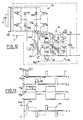
- FIG. 16 Another advantageous embodiment of a converter 3 implementing the method according to the invention is illustrated by the electrical diagram in FIG. 16.
- the converter 3 comprises a transformer TRS comprising a primary winding EPS supplied by a symmetrical bridge PS and two secondary windings ES1 and ES2 connected respectively to two secondary stages S10 and S20 having in common the bidirectional switching component TD4 and the oscillation capacitor C. Only the bidirectional switching components TD21 and TD22 are distinct. The respective outputs of the two stages S10, S20 are connected in parallel to a single output filter F itself connected at a charge Ch.
- control modes of the transistors of the primary stage and the secondary stages are identical to those studied in the previous version in which the two secondary stages were connected in series.
- the current IL has a bidirectional waveform characteristic of operation in a discontinuous conduction regime.
- the current ITR absorbed by the primary winding of the transformer is naturally equal to the sum of the secondary currents I1 and I2 multiplied by the transformation ratio m.
- the bidirectional current switching components TD2, TD4 can advantageously include insulated gate transistors, for example transistors called IGBT (Insulated Gate Bipolar Transistor) which involve both majority carriers (such as MOS transistors) and minority carriers (such as bipolar transistors).
- IGBT Insulated Gate Bipolar Transistor
- This type of component is particularly well suited to the production of converters implementing the method according to the present invention insofar as, in natural switching, it exhibits dynamic behavior compatible with the required switching frequencies (often greater than 100 kHz ).
- the physical characteristics of the main constituent elements of the converter, namely the transformer and the oscillation capacitor determine the natural frequency Fo of the oscillating circuit (L, C). (A numerical example recorded experimentally thus gives a frequency value of 275 kHz). On this natural frequency depends the duration of the direct conduction phase CD which is substantially equal to 1 / Fo.
- a converter in accordance with the invention has already been produced and tested. Powered by a 450 V DC network, it delivers a power of 2 kW at a nominal voltage of 100 V (nominal current 20 A) with a switching frequency of 90 kHz.
- bidirectional current switching components can be made with transistors of any technology, if these satisfy the requirements for correct operation at high frequency and can be controlled in a simple manner.
- new developments in insulated gate transistors operating at high frequency and high voltage can effectively contribute to the production of DC-DC converters. implementing the process according to the invention always more efficient.
Landscapes
- Engineering & Computer Science (AREA)
- Power Engineering (AREA)
- Dc-Dc Converters (AREA)
Claims (11)
- Verfahren zur Linearisierung der Ausgangskennwerte (Spannung/Strom) eines pseudoresonanten Gleichstrom-Gleichstrom-Wandlers (1) mit direktem Energietransfer, wobei der Wandler einen Transformator (TR) mit einer Primärwicklung (EP) und einer Sekundärwicklung (ES), der von einem Strom (I2) durchflossen wird, und einen Schwingkreiskondensator (C) enthält und vorbestimmten Steuerzyklen (CY) unterliegt, die je eine Direktleitphase (CD) enthalten, dadurch gekennzeichnet, daß während jedes Zyklus nacheinander- die vollständige Entladung (ED) des Schwingkreiskondensators (C), unabhängig vom Ausgangsstrom, beginnend spätestens am Ende jeder Direktleitphase (CD),- und das Halten der Spannung (Vc) an den Klemmen des Kondensators (C) bis zum Beginn der nächsten Leitphase auf einem Wert von praktisch null Volt erfolgen,- wobei die vollständige Entladung (ED) des Kondensators (C) einen Verfahrensschritt (ED1), der während der Direktleitphase (CD) abläuft und nach der Umkehr des Stroms (Ic) im Kondensator (C) beginnt, und einen nachfolgenden Verfahrensschritt (ED2) enthält, der am Ende der Direktleitphase (CD) beginnt und mit der Annulierung der Spannung (VC) an den Klemmen des Kondensators (C) endet.
- Verfahren zur Linearisierung nach Anspruch 1, dadurch gekennzeichnet, daß die Haltephase (EM) einen ersten Verfahrensschritt (EME), in dem die Spannung (Vc) an den Klemmen des Kondensators (C) durch Haltemittel (TD4) während einer vorbestimmten Zeit (TM) wirksam auf einem Wert von im wesentlichen null Volt gehalten wird und unmittelbar anschließend einen zweiten, Sicherheitsverfahrensschritt (ES) aufweist, der bis zum Beginn der nächsten Direktleitphase (CD) abläuft und in dem die Haltemittel (TD4) nicht aktiviert sind.
- Pseudoresonanter Gleichstrom-Gleichstrom-Wandler (1, 2, 3) mit Direkttransfer, der Transformatoren (TR, TR1, ... TRN) mit je einer Primärwicklung (EP), die an eine Primärstufe (P) angeschlossen ist, und mit Sekundärwicklungen (ES), die je an eine Sekundärstufe (S) mit einem Schwingkreiskondensator (C) angeschlossen sind, ein Bauteil mit nur einer Leitrichtung (D4), das parallel zum Kondensator (C) geschaltet ist, und ein Bauteil mit nur einer Leitrichtung (D2) in Reihe mit der Sekundärwicklung (ES) und dem Kondensator (C) aufweist, dadurch gekennzeichnet, daß jede der Sekundärstufen weiter aufweist:- ein Schaltelement (T2), das parallel zu dem Bauelement mit nur einer Leitrichtung (D2) liegt, welches mit der Sekundärwicklung (ES) und dem Kondensator (T) in Reihe angeordnet ist, und mit dem Bauelement (D2) mit nur einer Leitrichtung so zusammenwirkt, daß sich ein in beiden Stromrichtungen wirkendes bidirektionales Schaltelement (TD2) ergibt,- und ein Schaltelement (T4), das parallel zum Schwingkreiskondensator und dem Bauelement mit nur einer Leitrichtung (D4) geschaltet ist und mit letzterem so zusammenwirkt, daß sich ein in beiden Stromrichtungen wirkendes Schaltelement (TD4) ergibt.
- Gleichstrom-Gleichstrom-Wandler (1, 2, 3) nach Anspruch 3, der vorgegebenen Steuerzyklen (CY) mit je einer direkten Leitphase (CD) unterworfen ist, dadurch gekennzeichnet, daß jede Sekundärstufe (S) Steuermittel (MC) für die in beiden Stromrichtungen wirkenden Schaltelemente (TD2, TD4) aufweist, die einerseits eine vollständige Entladung des Schwingkreiskondensators (C) am Ende der Direktleitphase (CD) und andererseits bewirken, daß die Spannung (Vc) an den Klemmen des Kondensators (C) auf einem Wert von im wesentlichen null Volt gehalten wird.
- Gleichstrom-Gleichstrom-Wandler (1) nach Anspruch 4, mit einem Transformator (TR), dessen Primärwicklung (EP) und Sekundärwicklung (ES) mit einer Primärstufe (P) bzw. einer Sekundärstufe (S) verbunden sind, dadurch gekennzeichnet, daß die Primärstufe (P) eine unsymmetrische Halbbrücke (PA) enthält.
- Gleichstrom-Gleichstrom-Wandler (2, 3) nach Anspruch 4 mit einem Transformator (TR), der eine an eine Primärstufe (P) angeschlossene Primärwicklung (EP) und zwei Sekundärwicklungen (ES1, ES2) enthält, die je an eine Sekundärstufe (S1, S2) angeschlossen sind, dadurch gekennzeichnet, daß die Primärstufe (P) eine symmetrische Brücke (PS) enthält.
- Gleichstrom-Gleichstrom-Wandler (2) nach Anspruch 6, dadurch gekennzeichnet, daß die Sekundärstufen (S1, S2) elektrisch in Reihe geschaltet sind und daß der Wandler Mittel zur Steuerung dieser Stufen im verschachtelten Betrieb aufweist.
- Gleichstrom-Gleichstrom-Wandler (3) nach Anspruch 6, dadurch gekennzeichnet, daß die Sekundärstufen (S1, S2) elektrisch in Höhe des gemeinsamen Schwingkreiskondensators (C) parallelgeschaltet sind und daß der Wandler Mittel zur Steuerung dieser Stufen im verschachtelten Betrieb enthält.
- Gleichstrom-Gleichstrom-Wandler (3) nach Anspruch 8, dadurch gekennzeichnet, daß die in beiden Stromrichtungen wirkenden Schaltelemente jeder der Sekundärstufen (S1, S2) in einem einzigen in beiden Stromrichtungen wirkenden Schaltelement (TD4) zusammengefaßt sind.
- Gleichstrom-Gleichstrom-Wandler (1, 2, 3) nach einem der Ansprüche 4 bis 9, dadurch gekennzeichnet, daß die Steuermittel (MC) für die in beiden Stromrichtungen wirksamen Schaltelemente (TD2, TD4) Steuermittel (MT2) für das Schaltelement (T2), die mit Mitteln (D) zur Erfassung des Vorzeichens der Spannung (Vc) an den Klemmen des Schwingkreiskondensators (C) zusammenwirken, um das Schaltelement (T2) leitend zu machen, wenn die Spannung (Vc) größer als die Steuerschwelle des Schaltelements (T2) wird, und Steuermittel (MT4) für das Schaltelement (T4) aufweisen, die mit den Steuermitteln (MT2) und den Steuermitteln (MP) der Primärstufe (P) zusammenwirken, um das Schaltelement (T4) von der Sperrung des Schaltelements (T2) bis zum Beginn des nächstfolgenden Steuerzyklus (CY) leitend zu steuern.
- Gleichstrom-Gleichstrom-Wandler (1, 2, 3) nach einem der Ansprüche 3 bis 10, dadurch gekennzeichnet, daß die Schaltelemente (T2, T4) Transistoren mit isoliertem Gate sind.
Applications Claiming Priority (2)
| Application Number | Priority Date | Filing Date | Title |
|---|---|---|---|
| FR8807024A FR2632134B1 (fr) | 1988-05-26 | 1988-05-26 | Procede de linearisation pour convertisseur continu-continu et dispositifs mettant en oeuvre ce procede |
| FR8807024 | 1988-05-26 |
Publications (2)
| Publication Number | Publication Date |
|---|---|
| EP0344067A1 EP0344067A1 (de) | 1989-11-29 |
| EP0344067B1 true EP0344067B1 (de) | 1993-03-10 |
Family
ID=9366655
Family Applications (1)
| Application Number | Title | Priority Date | Filing Date |
|---|---|---|---|
| EP19890401417 Expired - Lifetime EP0344067B1 (de) | 1988-05-26 | 1989-05-24 | Linearisierungsverfahren für Gleichspannungswandler und Durchführung des Verfahrens |
Country Status (3)
| Country | Link |
|---|---|
| EP (1) | EP0344067B1 (de) |
| DE (1) | DE68905238T2 (de) |
| FR (1) | FR2632134B1 (de) |
Families Citing this family (7)
| Publication number | Priority date | Publication date | Assignee | Title |
|---|---|---|---|---|
| US5235502A (en) * | 1989-11-22 | 1993-08-10 | Vlt Corporation | Zero current switching forward power conversion apparatus and method with controllable energy transfer |
| CA2029209C (en) * | 1989-11-22 | 1999-07-27 | Patrizio Vinciarelli | Zero-current switching forward power conversion with controllable energy transfer |
| US5291385A (en) * | 1992-04-02 | 1994-03-01 | Vlt Corporation | Zero-current switching forward power converter operating in damped reverse boost mode |
| DE19711817A1 (de) * | 1997-03-21 | 1998-09-24 | Abb Daimler Benz Transp | Schaltnetzteil |
| FR2993114B1 (fr) * | 2012-07-04 | 2014-08-15 | Centre Nat Etd Spatiales | Systeme de conversion de puissance electrique modulaire a partir d'un pont asymetrique monophase a deux interrupteurs et deux diodes de roue libre avec diodes d'isolation. |
| DE102018106886B4 (de) * | 2018-03-22 | 2022-04-21 | Infineon Technologies Americas Corp. | Wandlerschaltung |
| CN117240106B (zh) * | 2023-11-16 | 2024-03-01 | 杭州蔚斯博系统科技有限公司 | 桥式谐振变换器及双向桥式谐振变换器 |
Family Cites Families (1)
| Publication number | Priority date | Publication date | Assignee | Title |
|---|---|---|---|---|
| US4415959A (en) * | 1981-03-20 | 1983-11-15 | Vicor Corporation | Forward converter switching at zero current |
-
1988
- 1988-05-26 FR FR8807024A patent/FR2632134B1/fr not_active Expired - Fee Related
-
1989
- 1989-05-24 DE DE1989605238 patent/DE68905238T2/de not_active Expired - Fee Related
- 1989-05-24 EP EP19890401417 patent/EP0344067B1/de not_active Expired - Lifetime
Also Published As
| Publication number | Publication date |
|---|---|
| FR2632134A1 (fr) | 1989-12-01 |
| EP0344067A1 (de) | 1989-11-29 |
| DE68905238D1 (de) | 1993-04-15 |
| FR2632134B1 (fr) | 1990-09-14 |
| DE68905238T2 (de) | 1993-06-17 |
Similar Documents
| Publication | Publication Date | Title |
|---|---|---|
| EP2442436B1 (de) | Verfahren und Steuersystem zur allgemeinen Reduzierung des Stroms in einem Leistungswandler | |
| EP2747266B1 (de) | Stromzuführungssystem mit Partitionierung, und ein solches System umfassendes Luftfahrzeug | |
| EP2276173B1 (de) | Treiber für einen Leistungstransistor | |
| FR2541531A1 (fr) | Procede pour creer un courant alternatif a partir d'un courant continu | |
| EP2833534B1 (de) | Antriebssystem mit aktivem Gleichrichter und Wechselrichter mit Pulsmodifikation zur Minimierung von Gleichtaktstörungen | |
| EP0344067B1 (de) | Linearisierungsverfahren für Gleichspannungswandler und Durchführung des Verfahrens | |
| EP0329571B1 (de) | Schaltungsanordnung zur Überwachung der Entmagnetisierung für einen Sperrwandler mit primärseitiger und secundärseitiger Regelung | |
| EP2320553B1 (de) | Stromumwandlungsvorrichtung und unterbrechungsfreie Stromversorgung, die eine solche Vorrichtung umfasst | |
| EP0670624B1 (de) | Angepasstes Schaltnetzteil um Kommutierungen bei niedriger Spannung auszuführen | |
| EP0821844B1 (de) | Verfahren zur verarbeitung von pulsbreitenmodulierten wellen und vorrichtung dafür | |
| WO2008009538A1 (fr) | Procede et dispositif de regulation d'un onduleur resonant, et onduleur resonant equipe d'un tel dispositif | |
| EP3373429A1 (de) | Dual active bridge umrichter und ansteuerverfahren | |
| EP1564876A1 (de) | Schweisseinrichtung mit sanfschaltendem Quasi-resonanzwechselrichter | |
| FR2804257A1 (fr) | Amplificateur de puissance rf et ses ameliorations | |
| FR3022090A1 (fr) | Circuit onduleur et son procede de gestion | |
| EP3687051B1 (de) | Resonanter llcc-konverter in serie und parallel | |
| EP4513736A1 (de) | Leistungsfaktor-korrekturschaltung | |
| EP0928057B1 (de) | Hochspannungsschalter aus reihengeschalteten resonanten Zellen | |
| FR2933546A1 (fr) | Poste de soudage a l'arc a onduleur a commutation douce quasi resonnant | |
| FR3063849A1 (fr) | Procede de commande d'un bras de commutation a au moins deux transistors de puissance a double grille et systeme de commande destine a mettre en oeuvre ledit procede | |
| FR3150367A1 (fr) | Convertisseur électrique continu-continu isolé, réseau électrique comprenant un tel convertisseur et procédé de conversion associé | |
| WO2024261125A1 (fr) | Convertisseur électrique continu-continu isolé, réseau électrique comprenant un tel convertisseur électrique et procédé de conversion associé | |
| FR2564655A1 (fr) | Convertisseur reversible de courant, et alimentation de secours le comprenant | |
| EP1039622A1 (de) | Verfahren zur Versorgung von galvanische Trennung benötigender Ausrüstung und entsprechender Generator | |
| FR2802730A1 (fr) | Procede de commande d'un convertisseur d'energie electrique du type alternatif-alternatif et dispositif de commande pour la mise en oeuvre du procede |
Legal Events
| Date | Code | Title | Description |
|---|---|---|---|
| PUAI | Public reference made under article 153(3) epc to a published international application that has entered the european phase |
Free format text: ORIGINAL CODE: 0009012 |
|
| 17P | Request for examination filed |
Effective date: 19890529 |
|
| AK | Designated contracting states |
Kind code of ref document: A1 Designated state(s): DE GB IT |
|
| 17Q | First examination report despatched |
Effective date: 19920115 |
|
| GRAA | (expected) grant |
Free format text: ORIGINAL CODE: 0009210 |
|
| AK | Designated contracting states |
Kind code of ref document: B1 Designated state(s): DE GB IT |
|
| ITF | It: translation for a ep patent filed | ||
| REF | Corresponds to: |
Ref document number: 68905238 Country of ref document: DE Date of ref document: 19930415 |
|
| GBT | Gb: translation of ep patent filed (gb section 77(6)(a)/1977) |
Effective date: 19930323 |
|
| PLBE | No opposition filed within time limit |
Free format text: ORIGINAL CODE: 0009261 |
|
| STAA | Information on the status of an ep patent application or granted ep patent |
Free format text: STATUS: NO OPPOSITION FILED WITHIN TIME LIMIT |
|
| 26N | No opposition filed | ||
| ITPR | It: changes in ownership of a european patent |
Owner name: CESSIONE;ALCATEL ALSTHOM COMPAGNIE GENERALE D'ELEC |
|
| REG | Reference to a national code |
Ref country code: GB Ref legal event code: 732E |
|
| PGFP | Annual fee paid to national office [announced via postgrant information from national office to epo] |
Ref country code: GB Payment date: 19970410 Year of fee payment: 9 |
|
| PGFP | Annual fee paid to national office [announced via postgrant information from national office to epo] |
Ref country code: DE Payment date: 19970510 Year of fee payment: 9 |
|
| PG25 | Lapsed in a contracting state [announced via postgrant information from national office to epo] |
Ref country code: GB Free format text: LAPSE BECAUSE OF NON-PAYMENT OF DUE FEES Effective date: 19980524 |
|
| GBPC | Gb: european patent ceased through non-payment of renewal fee |
Effective date: 19980524 |
|
| PG25 | Lapsed in a contracting state [announced via postgrant information from national office to epo] |
Ref country code: DE Free format text: LAPSE BECAUSE OF NON-PAYMENT OF DUE FEES Effective date: 19990302 |
|
| PG25 | Lapsed in a contracting state [announced via postgrant information from national office to epo] |
Ref country code: IT Free format text: LAPSE BECAUSE OF NON-PAYMENT OF DUE FEES;WARNING: LAPSES OF ITALIAN PATENTS WITH EFFECTIVE DATE BEFORE 2007 MAY HAVE OCCURRED AT ANY TIME BEFORE 2007. THE CORRECT EFFECTIVE DATE MAY BE DIFFERENT FROM THE ONE RECORDED. Effective date: 20050524 |