EP0345922A2 - Convertisseur numérique-analogique à commande par diode - Google Patents
Convertisseur numérique-analogique à commande par diode Download PDFInfo
- Publication number
- EP0345922A2 EP0345922A2 EP89302528A EP89302528A EP0345922A2 EP 0345922 A2 EP0345922 A2 EP 0345922A2 EP 89302528 A EP89302528 A EP 89302528A EP 89302528 A EP89302528 A EP 89302528A EP 0345922 A2 EP0345922 A2 EP 0345922A2
- Authority
- EP
- European Patent Office
- Prior art keywords
- diodes
- diode
- control
- circuits
- circuit
- Prior art date
- Legal status (The legal status is an assumption and is not a legal conclusion. Google has not performed a legal analysis and makes no representation as to the accuracy of the status listed.)
- Withdrawn
Links
Images


Classifications
-
- H—ELECTRICITY
- H03—ELECTRONIC CIRCUITRY
- H03M—CODING; DECODING; CODE CONVERSION IN GENERAL
- H03M1/00—Analogue/digital conversion; Digital/analogue conversion
- H03M1/66—Digital/analogue converters
- H03M1/74—Simultaneous conversion
- H03M1/80—Simultaneous conversion using weighted impedances
- H03M1/808—Simultaneous conversion using weighted impedances using resistors
-
- H—ELECTRICITY
- H03—ELECTRONIC CIRCUITRY
- H03M—CODING; DECODING; CODE CONVERSION IN GENERAL
- H03M1/00—Analogue/digital conversion; Digital/analogue conversion
- H03M1/66—Digital/analogue converters
- H03M1/74—Simultaneous conversion
-
- H—ELECTRICITY
- H03—ELECTRONIC CIRCUITRY
- H03M—CODING; DECODING; CODE CONVERSION IN GENERAL
- H03M1/00—Analogue/digital conversion; Digital/analogue conversion
- H03M1/66—Digital/analogue converters
- H03M1/74—Simultaneous conversion
- H03M1/742—Simultaneous conversion using current sources as quantisation value generators
- H03M1/745—Simultaneous conversion using current sources as quantisation value generators with weighted currents
Definitions
- This invention relates to digital-to-analog converters (DACs), and more particularly to DACs implemented as integrated circuits.
- DACs digital-to-analog converters
- FIG. 1 A basic type of DAC, referred to as a weighted R device, is shown in FIG. 1. It consists of a series of binarily weighted resistors which are connected in common to one side to an output line 2, each resistor comprising one step of the ladder. For n steps, the resistor in the circuit for the most significant bit (MSB) has a value R, while the resistor in the circuit for the least significant bit (LSB) has a value 2 n-1 R.
- the resistance values for the intermediate bits are scaled binarily between the MSB and LSB.
- Each resistor can be connected by means of a switch 4 to either a ground line 6, or a common voltage reference line 8.
- the step circuits corresponding to the input bits having a digital 1 are connected to the voltage reference line 8, while the step circuits corresponding to the bits having a digital 0 are connected to the ground line 6.
- an output signal equal to the weighted sum of the currents flowing through the various steps connected to the voltage reference line 8 will appear on output line 2.
- This signal is amplified and converted to an output voltage signal V0 by means of amplifier 10 having a feedback resistor R F .
- weighted R circuit is simple in design, a large number of resistors are required to give it a useful range; the higher value resistors can become quite large and occupy undesirably amounts of area on the chip.
- FIG. 2 Another type of conventional DAC, referred to as an R-2R ladder device, is shown in FIG. 2.
- the various steps have equal value 2R resistors.
- the input sides of the circuits are switched between a voltage reference line 8 and a ground line 6 by means of switches 4 in a manner similar to the weighted R device of FIG. 1.
- the output sides of successivelysive steps are connected to each other through additional resistors of resistance value R, with the output of the LSB connected to ground through a 2R resistor.
- An output analog voltage V0 is obtained from the output of the MSB through amplifier 10 with feedback resistor R F .
- the switch for the MSB step is controlled directly by the most significant bit of the input digital signal, the switch for the next most significant step is controlled by the second most significant bit of the input digital signal, and so forth.
- a binary relationship is established between successive bits of the R-2R ladder circuit. While it is more economical for the number of resistors required than is the weighted R circuited of FIG. 1, it still requires switching between two definite voltage levels, and is subject to substantial temperature variations.
- FIG. 3 A different design, referred to as a segmented DAC, is shown in FIG. 3. Again, individual ladder steps circuits are switched between a voltage reference line 8 and a ground line 6. As in the designs of FIGs. 1 and 2, MOS switches are typically employed. The ladder steps each have the same resistance R, and are connected in parallel between the voltage reference/ground lines 8/6 and the output line 2. A very large number of step resistance circuits, equal to 2 n-1 , are used, where n is equal to the number of bits in the input digital signal.
- a decode logic circuit 12 is provided which converts the input digital signal, consisting of bits B1-Bn, into a control signal which connects the appropriate number of steps to the voltage reference line 8. For example, for an 8 bit input digital signal with 511 different possible values, 511 separate step circuits would be provided, and the number of steps connected to the voltage reference line at any time would equal the value of the input digital signal.
- the segmented DAC requires an extremely large number of resistors, which increases geometrically with the number of bits in the input digital signal. Also, because switching occurs over a relatively large voltage range between V REF and ground, switching is still relatively slow because of the capacitance associated with practical semiconductor switches.
- FIG. 4 A modification of the FIG. 3 approach which attempts to compensate for its slow switching speed is shown in FIG. 4.
- the switches 4 are moved to the output side of the resistors, and therefore do not have to switch all the way between the voltage reference and ground. While this design offers some improvement and is in common use in many CMOS DACs, the capacitance associated with practical switches degrades the phase margin of the amplifier, leading to a requirement for extremely low capacitance switches to obtain high speed performance.
- Bipolar transistor switches offer faster switching speeds than most MOS transistors because the bipolar devices are smaller.
- a conventional DAC design using bipolar transistors is shown in FIG. 5.
- a ladder network is provided with resistors having equal resistance values for a segmented device, or weighted resistance values for a weighted ladder; an R-2R ladder can also be used.
- the network is referenced to a negative voltage level obtained from the positive voltage reference line 8, via inverting amplifier 14.
- Transistor Q1 is a compensating element for transistors Q2-Q4, which provide current sources for accumulated an analog output.
- the resistor ladder network divides the currents through the transistors Q2-Q4 such that the current through each transistor is decremented by a predetermined portion of the current through the preceding transistor for a weighted ladder, or is equal to the other transistor currents for a segmented ladder.
- the base-emitter junctions of transistors Q1-Q4 are geometrically scaled in a weighted ladder to offset the effect of the different current levels, which otherwise would produce a different V be for each transistor.
- Each of the bit transistors Q2-Q4 is supplied through a respective pair of bipolar switching transistors, with Q5 and Q6 supplying Q2, Q7 and Q8 supplying Q3, and Q9 and Q10 supplying Q4.
- the outputs of Q5, Q7 and Q9 are connected to ground and are actuated when no output is desired from their respective bits, while the outputs of Q6, Q8 and Q10 are connected to an output line 2.
- Q1 compensates for the ⁇ error associated with Q2-Q4, where ⁇ equals 1-1/ ⁇ , and ⁇ is the transistor current gain.
- another bipolar transistor Q11 is provided between voltage reference line 8 and Q1 to compensate for the ⁇ error associated with Q6, Q8 and Q10. Any mismatches of ⁇ between the various transistors are not compensated, but can generally be overcome by trimming the resistors. However, since ⁇ is dependent upon ⁇ , and ⁇ varies by a factor of about 1:3 over the military specification temperature range of -55°C to +125°C, the ⁇ errors cannot be trimmed out over this temperature range. This can lead to serious operating problems, especially with DACs of over 12 bits. In some cases the transistor switches Q5-Q10 have been replaced with diode switches, but ⁇ still has a significant temperature variation because the DAC currents still have to pass through transistors Q1-Q4.
- the object of the present invention is to provide a novel DAC which has high speed operation, is accurate and relatively temperature insensitive, is not wasteful of power or chip space, and can accommodate a large number of bits.
- each step circuit includes a control diode that controls the flow of current through the step in accordance with a corresponding control signal from an associated actuating circuit.
- a single diode is employed on the output side of each ladder resistor. The resistance values and diode areas are weighted for a weighted ladder design, and equal for a segmented ladder.
- a control diode is connected on the output side of each ladder resistor, and a second diode is connected on the voltage reference side.
- the resistors are weighted, but a corresponding weighting of the control diodes is avoided by providing the second diodes with a double weighting.
- Another variation also uses second diodes in each step circuit, but allows them to have equal areas by also providing a current source for each step circuit which injects a predetermined amount of current into the second diode so that the various step circuits conduct their intended levels of current.
- the current sources are scaled in proportion to 2 (b-1) , where b is the order of the step circuit in which the current source is located.
- control diodes implemented as bipolar transistors, having their bases and collectors connected together, a further enhancement is achieved by making the base-collector connection at a location remote from the diodes by means of metallic base and collector leads that are electrically isolated from each other in the vicinity of the diodes.
- Metallization resistances associated with the leads thereby effect the step currents generally only in proportion to the transistor base currents, rather than in proportion to the collector currents, while the transistors remain unsaturated.
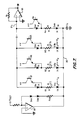
- FIG. 6 shows one embodiment of the present invention in which control diodes are introduced into the DAC step circuits to overcome the various problems with prior DACs. Only a segment of a DAC ladder is shown, consisting of resistors R1, R2, R3 and Rn. Similar circuitry would be provided for the remaining steps of the full DAC.
- FIG. 6 is adaptable to both segmented ladders and weighted ladders.
- a corresponding segmented ladder would have 2 n-1 steps.
- the resistor values are scaled in proportion to 1/2 ( n +1-b) , where b is the order of the step, b being equal to one for the most significant bit and equal to n for the least significant bit.
- the weighted ladder resistance values are indicated to the left of resistors R1-Rn in FIG. 6.
- R1-Rn For a segmented DAC all of the resistance values would be equal, as indicated by the common resistance value R to the right of each of the resistors R1-Rn.
- An R-2R ladder could also be used.
- diodes D1-Dn are connected in series with each of the step resistors R1-Rn, respectively.
- the diodes are located on the output sides of their corresponding resistors, and conduct current in a direction toward the resistors.
- the other sides of the diodes D1-Dn are connected together via common output line 2 to the output amplifier 10, which produces an analog output signal representing the sum of the signals from each of the individual step circuits at any particular time.
- the diodes D1-Dn are preferably implemented as bipolar transistors with their bases and collectors connected together. Their base-emitter junctions are geometrically scaled so that their areas vary inversely with the amount of current for each bit, thereby keeping the voltage drops across the various bit diodes substantially equal.
- the diode sizes are scaled in proportion to 2 (n-b) for a weighted ladder, as indicated by the scalings to the left of each diode symbol in FIG. 6 (x is a unit diode area).
- x is a unit diode area
- decode logic circuit 16 Current flow through each of the various step circuits is controlled by a decode logic circuit 16 and a series of transistors switches S1, S2, S3, Sn associated with the respective bit circuits.
- decode logic circuit 16 would simply furnish switch signals to each step circuit representing the "1" or "0" state if the input digital bit corresponding to that step circuit.
- each switch comprises a bipolar transistor having its collector connected to a positive voltage bus, its emitter connected to the cathode of its respective control diode, and its base supplied with a control signal from decode logic circuit 16.
- a +0.5 volt signal is delivered to its corresponding switch from the decode logic circuit, turning the switch "on”. This permits current to flow through the switch from the positive voltage bus to supply the step current, thereby raising the voltage at the diode cathode to hold the diode "off” and prevent any output current from the step.
- a step is turned “on” by applying a -0.5 volt signal from the decode logic circuit to its base. This holds the switch "off”, thereby permitting the step current to be supplied through the control diode and appear as an output from the DAC.
- the lower end of the ladder circuit is maintained at a negative voltage by means of a negative feedback loop consisting of an op amp 18 with a resistor R FB and compensating diode Dc in its feedback circuit.
- the inverting input of amplifier 18 is connected to a positive voltage reference, so that a negative reference appears at its output along negative reference line 20.
- the presence of compensating diode Dc in the feedback circuit adds a negative base-emitter voltage drop to the negative reference level, thereby compensating for the voltage drops across step diodes D1-Dn.
- a smoothing capacitor Cs is also connected to the negative voltage line 20 to smooth switching glitches.
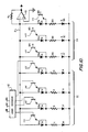
- FIG. 7 A variation of the circuit which permits a larger number of weighted steps without an accompanying loss of operating speed is shown in FIG. 7, with the same reference numerals used for common elements.
- a pair of diodes are used, one on each side of the resistor.
- the diodes D1a-Dna on the output side of the resistors have equal geometric scalings 1x.
- the diodes D1b-Dnb on the negative reference side of the resistors however, have a large scaling ratio 2 2(n-b) .
- the lower diodes increase in size by a factor of 4 from step to step.
- FIG. 7 circuit could also be implemented as a segmented ladder, with equal resistance values and lower diode scalings; the segmented values are indicated to the left of the resistors and lower diodes.
- a logic decode circuit used with a segmented version is not shown.
- the upper diodes Since the upper diodes have a common small scaling of 1x, they exhibit a low level of capacitance and do not interfere materially with operating speed. On the other hand, the lower diodes for the more significant bits have a high capacitance. However, since the lower diodes are on the negative reference side of the resistors R1-Rn, they are subject to only small voltage swings. Therefore, they can become quite large without slowing the switching speed significantly.
- FIG. 7 While the circuit of FIG. 7 has a lower output capacitance than that of FIG. 6 and can accommodate a greater number of steps without sacrificing switching speed, the large area required by the lower diodes as the number of steps increases imposes a practical limitation. This problem is effectively resolved with the use of much smaller diodes in accordance with the circuit of FIG. 9.
- the reference, output, and logic decode circuits have not been shown, but would be provided comparable to those in FIGs. 6 and 7.
- the lower diodes D1b-Dnb are held to a common scaling of 1x by the addition of current sources I1, I2, I3, In, which supply predetermined current levels to the lower diodes for their respective steps.
- the magnitudes of the current sources are selected so that the variation in voltage drops across the lower diodes for the various steps will be the reverse of and balance out the variation in voltage drops across the upper diodes.
- the current sources are scaled in proportion to 2 n-1 for a binary weighted ladder.
- the current source I1 for the first step supplies a current I which is equal to the output current from that step.
- I will be in the range of a few hundred nanoamps to several miliamps.
- FIG. 10 illustrates the combination of a segmented ladder portion and a weighted ladder portion, both using the scheme of FIG. 7; a segmented ladder portion from FIG. 7 could also be combined with a weighted ladder portion from FIG. 9.
- a seven-step ladder capable of accepting six input digital bits is illustrated for simplicity, but normally a considerably larger device would be implemented.
- the three most significant input digital bits, B1, B2 and B3, are supplied to logic decoder 12, which outputs switching signals to four steps of a segmented ladder 22.
- the less significant bits B4, B5 and B6 control the switching of corresponding step circuits in the weighted ladder portion 24.
- An output signal will be accumulated on output line 2 which represents the arithmetic sum of the segmented circuits that have been switched "on” by logic decoder 12, plus the weighted outputs of any steps from the weighted ladder portion 24 that have been switched "on". In this manner, rapid switching rates can be maintained with a large number of input digital, without significant problems of excessive use of power or chip area.
- the metallization patterns used to connect the diode-connected transistors have associated metallization resistances that can introduce errors into the step currents.
- FIG. 11 The situation is illustrated in FIG. 11, in which the diodes D1a, D2a, D3a and D4a have been isolated.
- the diodes are implemented by bipolar transistors whose collectors have been connected to their bases.
- the bases of the various diodes are in series, with metallization resistances MR inherently associated with the connections therebetween.
- These metallization resistances are in series with the bit resistors, and therefore can introduce errors into the bit currents.
- FIG. 12 Rather than connecting the collector and base of each diode transistor at the site of each device, a single connection 26 for each of the devices is made at a location remote from the diodes by means of metallic base and collector leads 28, 30, which are electrically isolated from each other in the vicinity of the diodes.
- the base lead 30 will have metallization resistances MR associated with each diode, as will the collector lead 30. This will result in relatively large voltage drops across the collector metallization resistances, but these voltage drops will not change the bit currents so long as the diodes are not saturated, which is normally the case.
- the step currents will vary with the base-emitter voltage of each diode (V be ), which in turn varies with the base current.
- the metallization resistances in the base lead 28 will effect the base currents, but since the base current is less than the collector current by a factor equal to the diode-transistor current gain ⁇ , the step current error for each step caused by metallization resistances will also be reduced by a factor of about ⁇ . Since ⁇ is typically about 100, the current errors will be mostly eliminated.
Landscapes
- Engineering & Computer Science (AREA)
- Theoretical Computer Science (AREA)
- Analogue/Digital Conversion (AREA)
Applications Claiming Priority (2)
| Application Number | Priority Date | Filing Date | Title |
|---|---|---|---|
| US07/204,589 US4888589A (en) | 1988-06-09 | 1988-06-09 | Digital-to-analog converter with diode control |
| US204589 | 1988-06-09 |
Publications (2)
| Publication Number | Publication Date |
|---|---|
| EP0345922A2 true EP0345922A2 (fr) | 1989-12-13 |
| EP0345922A3 EP0345922A3 (fr) | 1992-10-21 |
Family
ID=22758558
Family Applications (1)
| Application Number | Title | Priority Date | Filing Date |
|---|---|---|---|
| EP19890302528 Withdrawn EP0345922A3 (fr) | 1988-06-09 | 1989-03-15 | Convertisseur numérique-analogique à commande par diode |
Country Status (3)
| Country | Link |
|---|---|
| US (1) | US4888589A (fr) |
| EP (1) | EP0345922A3 (fr) |
| JP (1) | JPH02104025A (fr) |
Families Citing this family (11)
| Publication number | Priority date | Publication date | Assignee | Title |
|---|---|---|---|---|
| JPH0284442U (fr) * | 1988-12-16 | 1990-06-29 | ||
| US5404143A (en) * | 1991-06-12 | 1995-04-04 | Intellectual Property Development Associates Of Connecticut, Inc. | Network swappers and circuits constructed from same |
| US5762072A (en) * | 1995-05-25 | 1998-06-09 | Conlan; Robert W. | Comparator apparatus and system for activity monitors |
| US6369734B2 (en) * | 1998-02-10 | 2002-04-09 | Intel Corporation | Method and apparatus for increasing linearity and reducing noise coupling in a digital to analog converter |
| US7088274B2 (en) * | 2002-04-09 | 2006-08-08 | Texas Instruments Incorporated | Difference amplifier for digital-to-analog converter |
| US7030790B1 (en) * | 2004-10-22 | 2006-04-18 | Broadcom Corporation | Systems and methods for auto gain control in Bi-CMOS digital to analog converters |
| JP4892368B2 (ja) * | 2007-02-06 | 2012-03-07 | 新日本無線株式会社 | 定電荷出力回路 |
| JP2008125124A (ja) * | 2008-02-01 | 2008-05-29 | Ricoh Co Ltd | 信号伝送装置 |
| US8350493B2 (en) * | 2009-02-06 | 2013-01-08 | Aerospace Optics, Inc. | Illuminated pushbutton switch with step dimming |
| US8860597B2 (en) * | 2011-07-06 | 2014-10-14 | Qualcomm Incorporated | Digital to-analog converter circuitry with weighted resistance elements |
| KR102553262B1 (ko) * | 2017-11-17 | 2023-07-07 | 삼성전자 주식회사 | 기준 전압 생성기 및 이를 포함하는 메모리 장치 |
Family Cites Families (12)
| Publication number | Priority date | Publication date | Assignee | Title |
|---|---|---|---|---|
| US3328792A (en) * | 1963-11-19 | 1967-06-27 | Dick Co Ab | Digital to analog converter |
| US3646587A (en) * | 1969-12-16 | 1972-02-29 | Hughes Aircraft Co | Digital-to-analog converter using field effect transistor switch resistors |
| US3610953A (en) * | 1970-03-03 | 1971-10-05 | Gordon Eng Co | Switching system |
| SU362459A1 (ru) * | 1971-05-24 | 1972-12-13 | В. Б. Реутов Ордена Ленина Институт кибернетики Украинской | •сесоюзиап i |
| US3815121A (en) * | 1972-12-01 | 1974-06-04 | Hybrid Syst Corp | Current mode digital-to-analog converter |
| US4016555A (en) * | 1975-04-07 | 1977-04-05 | Tyrrel Sylvan F | Signal converter |
| SU762164A1 (ru) * | 1978-07-10 | 1980-09-07 | Gennadij V Shejnin | Цифроаналоговый преобразователь 1 |
| JPS5827429A (ja) * | 1981-08-11 | 1983-02-18 | Matsushita Electric Ind Co Ltd | マイコン制御d/a変換装置 |
| DE3148956A1 (de) * | 1981-12-10 | 1983-06-23 | Siemens AG, 1000 Berlin und 8000 München | Integrierbare schaltung fuer digital/analog-wandler |
| JPS5979633A (ja) * | 1982-10-28 | 1984-05-08 | Toshiba Corp | 荷重抵抗回路による電流加算形デジタル/アナログ局部変換回路 |
| DE3333934A1 (de) * | 1983-09-20 | 1985-04-04 | Siemens AG, 1000 Berlin und 8000 München | Integrierbarer digital/analogwandler |
| JPS61198924A (ja) * | 1985-02-28 | 1986-09-03 | Canon Inc | 半導体回路 |
-
1988
- 1988-06-09 US US07/204,589 patent/US4888589A/en not_active Expired - Fee Related
-
1989
- 1989-03-15 EP EP19890302528 patent/EP0345922A3/fr not_active Withdrawn
- 1989-05-10 JP JP1117149A patent/JPH02104025A/ja active Pending
Also Published As
| Publication number | Publication date |
|---|---|
| JPH02104025A (ja) | 1990-04-17 |
| US4888589A (en) | 1989-12-19 |
| EP0345922A3 (fr) | 1992-10-21 |
Similar Documents
| Publication | Publication Date | Title |
|---|---|---|
| US4141004A (en) | Solid state digital to analog converter | |
| CA1234921A (fr) | Convertisseur numerique-analogique a grande resolution a deux etages | |
| JPS6238894B2 (fr) | ||
| WO1999026345A1 (fr) | Procede et circuit en echelle r/2r pour denumeriseur | |
| EP0311105A2 (fr) | Convertisseur analogique-numérique à division en sous-gammes ayant un convertisseur simultané à entrée symétrique | |
| EP0345922A2 (fr) | Convertisseur numérique-analogique à commande par diode | |
| US4521765A (en) | Circuit and method for reducing non-linearity in analog output current due to waste current switching | |
| US4309693A (en) | Solid state digital to analog converter | |
| US4482887A (en) | Integrated weighted current digital to analog converter | |
| US4034366A (en) | Analog-to-digital converter with controlled ladder network | |
| US3731181A (en) | Improved reference current source | |
| US5729231A (en) | Digital-to-analog converter having improved resistance to variations in DC current gain | |
| CA1114510A (fr) | Convertisseur numerique-analogique a courant pondere | |
| US4644325A (en) | Low voltage, single power supply operated digital analog converter | |
| US4468652A (en) | Digital-to-analog converter having ladder network and improved interconnection therefor | |
| US4551705A (en) | Programmable integrated circuit AC resistor network | |
| US4942397A (en) | Elimination of linearity superposition error in digital-to-analog converters | |
| EP1189353B1 (fr) | Convertisseur A/N | |
| US3717777A (en) | Digital to analog converter including improved reference current source | |
| US4831281A (en) | Merged multi-collector transistor | |
| US3932863A (en) | Digital-to-analog converters | |
| US4758820A (en) | Semiconductor circuit | |
| US5034630A (en) | Logic circuit for use in D/A converter having ECL-type gate structure | |
| EP0603904B1 (fr) | Circuit de conversion numérique-analogique | |
| JPH0777353B2 (ja) | デジタル・アナログ変換器 |
Legal Events
| Date | Code | Title | Description |
|---|---|---|---|
| PUAI | Public reference made under article 153(3) epc to a published international application that has entered the european phase |
Free format text: ORIGINAL CODE: 0009012 |
|
| AK | Designated contracting states |
Kind code of ref document: A2 Designated state(s): DE FR GB IT NL |
|
| PUAL | Search report despatched |
Free format text: ORIGINAL CODE: 0009013 |
|
| AK | Designated contracting states |
Kind code of ref document: A3 Designated state(s): DE FR GB IT NL |
|
| STAA | Information on the status of an ep patent application or granted ep patent |
Free format text: STATUS: THE APPLICATION IS DEEMED TO BE WITHDRAWN |
|
| 18D | Application deemed to be withdrawn |
Effective date: 19930422 |