EP0345971B1 - Anordnung, die eine optische oder opto-elektronische Vorrichtung enthält - Google Patents
Anordnung, die eine optische oder opto-elektronische Vorrichtung enthält Download PDFInfo
- Publication number
- EP0345971B1 EP0345971B1 EP89305312A EP89305312A EP0345971B1 EP 0345971 B1 EP0345971 B1 EP 0345971B1 EP 89305312 A EP89305312 A EP 89305312A EP 89305312 A EP89305312 A EP 89305312A EP 0345971 B1 EP0345971 B1 EP 0345971B1
- Authority
- EP
- European Patent Office
- Prior art keywords
- semiconductor material
- trapping layer
- electrons
- layer
- holes
- Prior art date
- Legal status (The legal status is an assumption and is not a legal conclusion. Google has not performed a legal analysis and makes no representation as to the accuracy of the status listed.)
- Expired - Lifetime
Links
Images


Classifications
-
- B—PERFORMING OPERATIONS; TRANSPORTING
- B82—NANOTECHNOLOGY
- B82Y—SPECIFIC USES OR APPLICATIONS OF NANOSTRUCTURES; MEASUREMENT OR ANALYSIS OF NANOSTRUCTURES; MANUFACTURE OR TREATMENT OF NANOSTRUCTURES
- B82Y20/00—Nanooptics, e.g. quantum optics or photonic crystals
-
- G—PHYSICS
- G02—OPTICS
- G02F—OPTICAL DEVICES OR ARRANGEMENTS FOR THE CONTROL OF LIGHT BY MODIFICATION OF THE OPTICAL PROPERTIES OF THE MEDIA OF THE ELEMENTS INVOLVED THEREIN; NON-LINEAR OPTICS; FREQUENCY-CHANGING OF LIGHT; OPTICAL LOGIC ELEMENTS; OPTICAL ANALOGUE/DIGITAL CONVERTERS
- G02F1/00—Devices or arrangements for the control of the intensity, colour, phase, polarisation or direction of light arriving from an independent light source, e.g. switching, gating or modulating; Non-linear optics
- G02F1/01—Devices or arrangements for the control of the intensity, colour, phase, polarisation or direction of light arriving from an independent light source, e.g. switching, gating or modulating; Non-linear optics for the control of the intensity, phase, polarisation or colour
- G02F1/015—Devices or arrangements for the control of the intensity, colour, phase, polarisation or direction of light arriving from an independent light source, e.g. switching, gating or modulating; Non-linear optics for the control of the intensity, phase, polarisation or colour based on semiconductor elements having potential barriers, e.g. having a PN or PIN junction
-
- G—PHYSICS
- G02—OPTICS
- G02F—OPTICAL DEVICES OR ARRANGEMENTS FOR THE CONTROL OF LIGHT BY MODIFICATION OF THE OPTICAL PROPERTIES OF THE MEDIA OF THE ELEMENTS INVOLVED THEREIN; NON-LINEAR OPTICS; FREQUENCY-CHANGING OF LIGHT; OPTICAL LOGIC ELEMENTS; OPTICAL ANALOGUE/DIGITAL CONVERTERS
- G02F1/00—Devices or arrangements for the control of the intensity, colour, phase, polarisation or direction of light arriving from an independent light source, e.g. switching, gating or modulating; Non-linear optics
- G02F1/01—Devices or arrangements for the control of the intensity, colour, phase, polarisation or direction of light arriving from an independent light source, e.g. switching, gating or modulating; Non-linear optics for the control of the intensity, phase, polarisation or colour
- G02F1/21—Devices or arrangements for the control of the intensity, colour, phase, polarisation or direction of light arriving from an independent light source, e.g. switching, gating or modulating; Non-linear optics for the control of the intensity, phase, polarisation or colour by interference
- G02F1/218—Devices or arrangements for the control of the intensity, colour, phase, polarisation or direction of light arriving from an independent light source, e.g. switching, gating or modulating; Non-linear optics for the control of the intensity, phase, polarisation or colour by interference using semi-conducting materials
-
- G—PHYSICS
- G02—OPTICS
- G02F—OPTICAL DEVICES OR ARRANGEMENTS FOR THE CONTROL OF LIGHT BY MODIFICATION OF THE OPTICAL PROPERTIES OF THE MEDIA OF THE ELEMENTS INVOLVED THEREIN; NON-LINEAR OPTICS; FREQUENCY-CHANGING OF LIGHT; OPTICAL LOGIC ELEMENTS; OPTICAL ANALOGUE/DIGITAL CONVERTERS
- G02F3/00—Optical logic elements; Optical bistable devices
- G02F3/02—Optical bistable devices
- G02F3/024—Optical bistable devices based on non-linear elements, e.g. non-linear Fabry-Perot cavity
-
- H—ELECTRICITY
- H01—ELECTRIC ELEMENTS
- H01S—DEVICES USING THE PROCESS OF LIGHT AMPLIFICATION BY STIMULATED EMISSION OF RADIATION [LASER] TO AMPLIFY OR GENERATE LIGHT; DEVICES USING STIMULATED EMISSION OF ELECTROMAGNETIC RADIATION IN WAVE RANGES OTHER THAN OPTICAL
- H01S5/00—Semiconductor lasers
- H01S5/30—Structure or shape of the active region; Materials used for the active region
- H01S5/34—Structure or shape of the active region; Materials used for the active region comprising quantum well or superlattice structures, e.g. single quantum well [SQW] lasers, multiple quantum well [MQW] lasers or graded index separate confinement heterostructure [GRINSCH] lasers
-
- H—ELECTRICITY
- H01—ELECTRIC ELEMENTS
- H01S—DEVICES USING THE PROCESS OF LIGHT AMPLIFICATION BY STIMULATED EMISSION OF RADIATION [LASER] TO AMPLIFY OR GENERATE LIGHT; DEVICES USING STIMULATED EMISSION OF ELECTROMAGNETIC RADIATION IN WAVE RANGES OTHER THAN OPTICAL
- H01S5/00—Semiconductor lasers
- H01S5/30—Structure or shape of the active region; Materials used for the active region
- H01S5/34—Structure or shape of the active region; Materials used for the active region comprising quantum well or superlattice structures, e.g. single quantum well [SQW] lasers, multiple quantum well [MQW] lasers or graded index separate confinement heterostructure [GRINSCH] lasers
- H01S5/3415—Structure or shape of the active region; Materials used for the active region comprising quantum well or superlattice structures, e.g. single quantum well [SQW] lasers, multiple quantum well [MQW] lasers or graded index separate confinement heterostructure [GRINSCH] lasers containing details related to carrier capture times into wells or barriers
-
- H—ELECTRICITY
- H01—ELECTRIC ELEMENTS
- H01S—DEVICES USING THE PROCESS OF LIGHT AMPLIFICATION BY STIMULATED EMISSION OF RADIATION [LASER] TO AMPLIFY OR GENERATE LIGHT; DEVICES USING STIMULATED EMISSION OF ELECTROMAGNETIC RADIATION IN WAVE RANGES OTHER THAN OPTICAL
- H01S5/00—Semiconductor lasers
- H01S5/30—Structure or shape of the active region; Materials used for the active region
- H01S5/34—Structure or shape of the active region; Materials used for the active region comprising quantum well or superlattice structures, e.g. single quantum well [SQW] lasers, multiple quantum well [MQW] lasers or graded index separate confinement heterostructure [GRINSCH] lasers
- H01S5/3415—Structure or shape of the active region; Materials used for the active region comprising quantum well or superlattice structures, e.g. single quantum well [SQW] lasers, multiple quantum well [MQW] lasers or graded index separate confinement heterostructure [GRINSCH] lasers containing details related to carrier capture times into wells or barriers
- H01S5/3416—Structure or shape of the active region; Materials used for the active region comprising quantum well or superlattice structures, e.g. single quantum well [SQW] lasers, multiple quantum well [MQW] lasers or graded index separate confinement heterostructure [GRINSCH] lasers containing details related to carrier capture times into wells or barriers tunneling through barriers
Definitions
- This invention pertains to the field of optical or opto-electronic devices, and to apparatus comprising such a device.
- optical and/or opto-electronic devices depend for their operation on the presence of a non-equilibrium (with respect to the device temperature) density of electrical carriers (electrons and/or holes) in at least a portion of the device, with the refractive index of the material depending on the density of carriers.
- a non-equilibrium with respect to the device temperature
- electrical carriers electro carriers
- the relevant portion of the device consists of semiconductor material, and the non-equilibrium carrier distribution is created by the absorption of electromagnetic radiation (resulting in the creation of electron/hole pairs).
- the non-equilibrium distribution can also be produced by injection of carriers into the portion of the device, e.g., by means of a p-n junction, as will be apparent to those skilled in the art.
- the rate at which the non-equilibrium carrier distribution can decay affects the speed at which the device can be operated, e.g., the minimum time between two signal pulses to which the device can respond. It is obviously desirable that the speed of operation be high, and thus it is important to have available means that can effect a speedy decay of a non-equilibrium carrier distribution in a relevant portion of an optical or opto-electronic device. This application discloses such means.
- bistable optical devices Bistable and other nonlinear optical devices have been known for some time, and a wide variety of signal processing functions can be carried out by means of bistable devices ("bistable” and “nonlinear” are used herein interchangeably unless indicated otherwise by the context).
- bistable optical logic devices both two-state and many-state
- bistable optical logic devices both two-state and many-state
- optical discriminators limiters
- pulse compressors oscillators
- gates and flip-flops
- nonlinear optical devices comprise a nonlinear Fabry-Perot (FP) etalon, a fixed-spacing optical cavity with, typically, an optically nonlinear medium within the cavity.
- FP Fabry-Perot
- solid (typically semiconductor, mostly GaAs-based) nonlinear media are, for instance, homogeneous GaAs, and GaAs-AlGaAs multiple quantum well (MQW) structures.
- a principal limitation on the operational speed of an optical device that comprises a nonlinear etalon is the recombination time of the hole/electron pairs created in the nonlinear spacer material of the device.
- the density of pairs in the relevant portion of the device has to decrease to a relatively small value (form the relatively high value required for the nonlinear action to occur) before another switching action can be initiated.
- PCT patent application WO84/03363 discloses a variety of Fabry-Perot etalons with quantum well superlattices disposed between the reflecting means of the etalon, and teaches that such etalons can exhibit optical bi-stability.
- the invention is embodied in apparatus as defined in claim 1 that comprises at least one optical or opto-electronic device comprising a first semiconductor material and at least one "trapping layer” (TL) in contact with the first semiconductor material, means for producing a non-equilibrium carrier distribution in at least a portion of the semiconductor material (exemplarily a source of electromagnetic radiation or a p-n junction), and means that are responsive to the density of electrons and/or holes in the first semiconductor material.
- a non-equilibrium density of electrons and/or holes is caused to be present in the first semiconductor material for a part of the time of operation, e.g., by exposure of the device to radiation from the radiation source.
- the TL is disposed substantially at a nodal plane of the radiation intensity distribution in the device whereby deleterious effects of the trapping layer (layers) on the optical properties of the device can be substantially avoided.
- the TL is a layer of a second material chosen such that at least one of the electrons and/or holes has a lower potential energy in the second material than in the first semiconductor material, whereby at least some of the carriers that enter the TL from the first semiconductor material are being trapped in the TL, whereby the density of carriers in the first semiconductor material is decreased.
- This decrease in the density of electrons and/or holes in the first semiconductor material can exemplarily result in a decrease of the time required by an optical switch or other device to reset, i.e., to be ready for a switching (or appropriate other) event subsequent to a first event.
- Other inventive devices may exhibit different beneficial characteristics due to the presence of one or more TLs, as will be discussed below in detail.
- material for use as TL is selected from the III-V semiconductors, the II-VI semiconductors, heavily doped Si and Ge, as well as metals and alloys such as NiAl.
- the device parameters e.g., location, thickness, composition of the trapping layer or layers
- the device parameters are chosen such that the probability of radiative recombination of electron/hole pairs in the trapping layer (layers) is substantially increased, whereby the heat sinking requirements for the device can be relaxed. Exemplary means for achieving this end will also be discussed below.
- the device comprises a Fabry-Perot etalon that comprises first and second reflector means, with the first semiconductor material and the TL layer disposed between the reflector means, or the device comprises a waveguide having a side surface, with the TL layer disposed parallel to said surface, at or close to the surface.
- FIG. 1 schematically depicts a portion of a prior art nonlinear etalon, wherein first reflecting means 14 (consisting of a multiplicity of layers 11 and 12, with 11 and 12 differing in refractive index) are positioned on substrate 10 (e.g., a GaAs wafer), and spacer body 13 (e.g., a GaAs layer of appropriate thickness) is formed on first reflecting means 14, with second reflecting means 15 (exemplarily, but not necessarily, also consisting of interspersed layers 11 and 12) formed on the spacer body.
- layers 11 are AlAs
- layers 12 GaAs are AlAs
- the thickness of each type of layer depends, inter alia, on the refractive index of the layer material and on the operating wavelength ⁇ o .
- the thickness of a layer is chosen to be ⁇ o /4n, where n is the refractive index of the layer material at ⁇ o .
- the optical properties of periodically stratified media of the type discussed herein are well known. See, for instance, M. Born and E. Wolf, Principles of Optics , 2nd edition (1964), pp. 68-70.
- multilayer dielectric mirrors including active mirrors
- inventive FP-etalons are not so limited, and all reflective means capable of creating an optical cavity are contemplated.
- the spacer body 13 typically is approximately of thickness ⁇ o /2n (or a multiple thereof). It generally, but not necessarily, consists of material that is optically active at ⁇ o .
- the second mirror resembles the first mirror but need not comprise the same combination of materials and/or contain the same number of layers.
- One or both of the multilayer mirrors may (but need not) comprise optically active material (at ⁇ o ).
- FIG. 2 schematically depicts a portion of an exemplary inventive etalon, and furthermore schematically indicates an exemplary field intensity distribution that may exit in the device if radiation of wavelength ⁇ o is coupled into the etalon.
- the inventive etalon comprises a multiplicity of TLs 22, exemplarily positioned such that the central plane of any given TL substantially coincides with a nodal plane 20 of the standing wave pattern 24.
- a "nodal plane” herein is a locus of minimum intensity in a standing wave field.
- Neighboring TLs are separated by spacer material 21, e.g., GaAs, with an inventive etalon comprising at least one, but typically a multiplicity of, TLs.
- the thickness of any given TL is substantially less than ⁇ o /2n, preferably less than about ⁇ o /10n, with the thickness chosen such that the TLs have substantially no effect on the radiation field in the optical cavity (when appropriately placed at nodal planes).
- the TL material and thickness are chosen such that at least one carrier type is confined in the TL with a confinement energy of at least about kT, where k is the Boltzmann constant and T is the absolute temperature.
- the active spacer layers 21 are GaAs and the TLs are 15 nm thick layers of In 0.25 Ga 0.75 As spaced 123 nm apart.
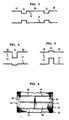
- the bandgap of a structure comprising alternate layers of GaAs and InGaAs is schematically shown in FIG. 3, wherein regions 30 and 31 are associated with GaAs and InGaAs, respectively, and numerals 32 and 33 refer to the conduction band edge and valence band edge, respectively.
- the bandgap of GaAs is about 1.4 eV, and that of In 0.25 Ga 0.75 As is about 1.0 eV.
- at room temperature kT is about 0.025 eV. This condition insures that at least a substantial portion of the carriers that are collected in a TL are confined to the TL for at least the recombination time.
- Monolithic inventive etalons of the type shown in FIG.2 can be fabricated by known techniques, typically comprising depositing on a planar major surface of an appropriate substrate the first reflecting means, thereon depositing the spacer body (comprising one or more TLs as well as the layers of the active material), and thereon depositing the second reflecting means, as well as, possibly, other layers.
- the sequence of depositions is carried out without intermittent handling of the wafer, e.g., in an MBE chamber with multiple sources.
- these steps may include deposition of a protective coating onto the top mirror, or coating of the top (and/or bottom) surface of the thus produced combinations with an appropriate resist, such that the top (and/or bottom) surface of the combination can then be patterned by methods well known in the semiconductor industry.
- a protective coating onto the top mirror or coating of the top (and/or bottom) surface of the thus produced combinations with an appropriate resist, such that the top (and/or bottom) surface of the combination can then be patterned by methods well known in the semiconductor industry.
- an array of FP etalons can be produced.
- Such an array can easily contain 100x100 etalons, and may contain 1000x1000 or even more etalons.
- the presence of one or more layers of relatively low bandgap material within the spacer body of a FP etalon results in accumulation of carrier pairs in the layer(s).
- the carriers which are created by photon excitation during a normal gating operation (primarily in the high bandgap material of the spacer body) diffuse in the material until they encounter a layer of low bandgap material (a TL), or until they recombine at a surface or within the volume of material. If they encounter a TL, there exists a significant probability that the carriers will penetrate into the TL and remain trapped therein.
- the TLs act as carrier sinks that remove carriers from active portions of the device, thereby speeding recovery of the device.
- inventive devices can use surface recombination in addition to TLs to speed recovery. As soon as a sufficient number of carriers is removed from the high-bandgap portion of the spacer body the device is ready for another gating operation.
- a device may require 1018 carriers/cm3 over a thickness of about 60 nm to operate and have a 30 ps cycle time.
- the lifetime in a 10 nm thick TL however might be 500 ps, so accumulated densities on the order of 1020cm ⁇ 3 (corresponding to 1014cm ⁇ 2 in the TL "quantum well") would be calculated.
- the actual lifetime (and, therefore, carrier density) in the TL typically however would be less.
- one or more TLs are positioned, and their parameters chosen, such that these TLs act to enhance radiative recombination, as compared to prior art devices lacking such TLs. That is to say, under identical operating conditions the number of radiative recombination events is larger in a preferred device according to the invention than it is in an otherwise identical device that lacks the means for enhancing radiative recombination.
- the peak luminescence wavelength ⁇ e of the TLs is substantially the same as the next-longer-wavelength transmission peak of the etalon (as is well known, a FP etalon has a series of narrow transmission peaks spaced apart in wavelength).
- a FP etalon has a series of narrow transmission peaks spaced apart in wavelength.
- the etalon can even act as a laser for the luminescence radiation ( ⁇ e > ⁇ o ), and thereby can maximize the amount of energy that is radiated out of the etalon rather than being dissipated as heat.
- the luminescence radiation typically will not affect operation of the apparatus, since the emitted wavelength differs from the operating wavelength ⁇ o . This is considered to be an important advantage of apparatus according to the invention.
- FIG.3 The bandgap relationship illustrated in FIG.3 is not the only possible one, and FIGS. 4 and 5 illustrate other exemplary relationships. If, as is illustrated in FIG. 4, both the conduction band edge and valence band edge of the TL material are below the respective edges of the contacting spacer material then electrons will be trapped in the usual manner in the TL, with the resulting localized charge imbalance attracting holes into the TL and also trapping them there.
- FIG. 5 illustrates the obverse situation, which results in trapping of holes in the usual manner, with electrons being bound electrostatically to the TL.
- the quantum "wells" in actual devices need (and frequently are) not as sharply defined as is shown in FIGS. 3-5, and instead may show accidental or intentional grading.
- accumulation of charge in a TL will result in a localized change in the shape of the band edges. This effect is well understood and does not require further discussion.
- the TL material will be a semiconductor this is not necessarily so. In particular, it may at times be advantageous to use a metal as the TL material.
- the metal is AlNi in combination with GaAs active spacer material. It is known that this combination of materials can be grown epitaxially, and in preferred devices the TL layer is epitaxial with the contacting spacer material.
- the device may be advantageous to design the device such that the trap or traps are relatively shallow (consistent with the previously stated criterion), especially if efficient energy removal through radiative recombination is considered to be important.
- the difference in carrier energy in the TL material and the active material will appear as thermal energy in the device, and only the bandgap energy of the TL material can be removed radiatively.
- TLs are placed into regions of relatively low radiation intensity.
- nodal planes are advantageous low intensity regions, and in devices that have a waveguide-like structure the region at (or close to) the lateral boundary of the device typically is a low intensity region.
- a TL frequently is advantageously placed at the lateral boundary of the device, with one side of the TL contacting the active material. Placement of TLs at the lateral boundary (which typically also is a low intensity region) may also be of advantage in some resonator-type devices, e.g., multiple quantum well (MQW) FP etalons.
- MQW multiple quantum well
- FIG. 6 shows a portion of a MQW device wherein barrier layers 60 alternate with well layers 61, with the side walls of the device comprising a TL 62 and a further layer 63, with the latter typically having a larger bandgap than the TL and serving to prevent surface recombination of carriers.
- TLs can be incorporated into quantum well devices. TLs need not be placed along the lateral boundary of such devices but can be placed parallel to the layers that form the MQW structure, despite the fact that longitudinal charge transport is restricted in such structures. Such transverse TLs are advantageously placed within or close to quantum wells. In the former case the TL (which advantageously is substantially thinner than the quantum well, typically less than 25% of the thickness of the well) may in principle be placed anywhere within the well, but may be advantageously placed at or close to a "wall" of the well, since in this case the presence of the TL will have a relatively small effect on the optical properties of the device. Such an arrangement is schematically illustrated in FIG.
- numerals 70,71 and 72 refer to barrier layer, well, and TL, respectively, and 73 and 74 refer to the conduction and the valence band edges, respectively.
- Dotted lines 75 and 76 indicate an exemplary probability distribution of electrons and holes, respectively, in the well. If the TL is placed outside the quantum well then it is advantageously placed close to the well such that a significant probability exists that carriers can tunnel from the well into the TL.
- the non-equilibrium carrier distribution in a device according to the invention can be produced by any appropriate method, including carrier injection by means of a p-n junction.
- a prior art FP etalon that comprises means for applying a reverse bias voltage to the etalon to affect its optical performance, see U. S. Patent 4,518,934.
- a voltage can be applied to an inventive device not only for purpose of carrier injection but also to speed existing carriers towards and into a TL, as will be recognized by those skilled in the art.
- means can be provided for setting up an electric field in an inventive device.
- the field direction may, for instance, be in generally a longitudinal or a transverse direction, and typically will comprise one or more electrodes and/or reverse biased junctions.
- the movement of carriers towards TLs can also be speeded by appropriate compositional grading of the active material.
- TLs may constitute the main means for speeding up the decay of a non-equilibrium carrier distribution, or surface recombination may constitute a further significant mechanism for speeding the decay.
- means may be provided for suppressing surface recombination (e.g., a surface layer of large bandgap material as depicted in FIG. 6). This may, for instance, be advantageously used with TLs that are designed to enhance radiative recombination.
- inventive devices can be fabricated on a InP substrate, with InGaAsP or InGaAs active material, and InAs TLs. Such devices can be transparent for wavelengths of about 1»m and larger.
- TLs can be viewed broadly as means for tailoring the characteristics of an optical or opto-electronic device. For instance, by incorporating TLs into an optical detector such as a PIN photo diode, the detector response amplitude can be enhanced if the TLs are parallel to the current flow, and the response speed can be increased if the TLs are perpendicular to the current flow.
- an optical detector such as a PIN photo diode
- FIG. 8 schematically depicts elements of exemplary apparatus according to the invention.
- the apparatus comprises a source 80 of "input" radiation of wavelength ⁇ i , a source 81 of "probe” radiation of wavelength ⁇ p , half-silvered mirrors 82 and 83, a FP-etalon according to the invention 85, a filter 86 and a radiation detector 84.
- ⁇ p and ⁇ i are selected such that the nonlinearity of the etalon is relatively small at ⁇ p and large at ⁇ i . Either one of ⁇ p and ⁇ i can be identified with ⁇ o . If only probe radiation is directed at the etalon then there is substantially no reflected radiation.
- the optical state of the etalon can change such that a substantial amount of reflected probe radiation is present, and can be detected by means of the detector, resulting in an output indicative of the optical state of the etalon.
- the etalon contains GaAs active material
- ⁇ i and ⁇ p exemplarily are 868 and 873 nm, respectively.
- other active materials e.g., InGaAsP and related compounds
- apparatus typically comprises a multiplicity of individually addressable devices, e.g., etalons comprising TLs.
- a multiplicity of etalons is made substantially as described in Example 2 of U. S. patent 4,756,606, except that the spacer body contains 9 TLs, substantially as described in Example 1 above.
- a metal TL optionally can also serve as a mirror in a FP etalon, or electrical contact can be made to the metal FP, e.g., to provide an electric field that can assist in moving carriers from the first semiconductor material into a TL.
Landscapes
- Physics & Mathematics (AREA)
- Nonlinear Science (AREA)
- Optics & Photonics (AREA)
- General Physics & Mathematics (AREA)
- Chemical & Material Sciences (AREA)
- Engineering & Computer Science (AREA)
- Nanotechnology (AREA)
- Biophysics (AREA)
- Life Sciences & Earth Sciences (AREA)
- Crystallography & Structural Chemistry (AREA)
- Condensed Matter Physics & Semiconductors (AREA)
- Electromagnetism (AREA)
- Semiconductor Lasers (AREA)
- Led Devices (AREA)
Claims (17)
- Optische Vorrichtung mit folgenden Merkmalen:a) einer Quelle (z.B. 80 oder 81) für elektromagnetische Strahlung der Wellenlänge λo;b) zumindest eine optische oder optoelektronische Vorrichtung (z.B. 85) umfassendi) eine bestimmte Menge eines ersten Halbleitermaterials (21) undii) zumindest eine Schicht aus einem zweiten Material (22), die als "Einfangschicht" bezeichnet wird und mit dem ersten Halbleitermaterial in Kontakt steht, wobei die Quelle und die Vorrichtung so angeordnet sind, daß die Vorrichtung zumindest während eines Teils der Zeit, in der die Apparatur betrieben wird, der Strahlung von der Quelle ausgesetzt ist, wobei diese Bestrahlung der Vorrichtung zu einer räumlich ungleichmäßigen Intensität der Strahlung in der Vorrichtung führt, die zumindest einen Bereich relativ geringer Strahlungsintensität aufweist;c) eine Einrichtung (z.B. 80 und/oder 81), um in dem ersten Halbleitermaterial eine Nichtgleichgewichtsdichte von Elektronen und/oder Löchern zu erzeugen, wobei das zweite Material so ausgewählt wird, daß zumindest eines der Elektronen und/oder Löcher in dem zweiten Material eine geringere potentielle Energie aufweist als in dem ersten Halbleitermaterial, so daß zumindest einige der Elektronen und/oder Löcher, welche von dem ersten Halbleitermaterial aus in die Einfangschicht eindringen, in der Einfangschicht eingefangen werden, wodurch die Nichtgleichgewichtsdichte der Elektronen und/oder Löcher in dem ersten Halbleitermaterial verringert werden kann;d) eine Einrichtung (z.B. 84), die auf ein optisches Ausgangssignal der Vorrichtung anspricht, welches von der Dichte der Elektronen und/oder Löcher in dem ersten Halbleitermaterial abhängt,
dadurch gekennzeichnet,
daß die Quelle und die Vorrichtung so angeordnet sind, daß sich zumindest eine Einfangschicht im wesentlichen in dem Bereich mit geringer Intensität befindet. - Vorrichtung nach Anspruch 1, bei der das zweite Material ein Metall oder ein zweites Halbleitermaterial ist und bei der mit dem ersten und zweiten Halbleitermaterial eine erste bzw. zweite Energie-oder Bandlücke zugeordnet ist, wobei die zweite Bandlücke um zumindest kT kleiner ist als die erste Bandlücke, wobei k die Boltzmann-Konstante und T die absolute Temperatur des ersten Halbleitermaterials ist.
- Vorrichtung nach Anspruch 2, bei der das erste Halbleitermaterial aus der aus GaAs und InGaAsP bestehenden Gruppe ausgewählt wird und das zweite Halbleitermaterial aus einer Gruppe ausgewählt wird, welche die III-V-Halbleiter, die II-VI-Halbleiter, stark dotiertes Silicium und stark dotiertes Germanium umfaßt.
- Vorrichtung nach Anspruch 1, bei der das erste Halbleitermaterial eine Mehrfach-Quanten-Well-Struktur umfaßt, die aus sich abwechselnden Halbleitermaterialschichten mit einer relativ großen bzw. einer relativ kleinen Bandlücke besteht, wobei eine Schicht aus dem Material mit der kleinen Bandlücke als "Well" oder "Mulde" bezeichnet wird.
- Vorrichtung nach Anspruch 4, bei der die Einfangschicht in einer Halbleitermaterialschicht mit relativ kleiner Bandlücke angeordnet ist, wobei das zweite Material entweder ein Metall oder ein Halbleiter ist, dessen Bandlücke kleiner als die Bandlücke des Halbleitermaterials mit relativ kleiner Bandlücke ist oder wobei die Einfangschicht in einer Halbleitermaterialschicht mit einer relativ großen Bandlücke in der Nähe eines Wells angeordnet ist, so daß die Elektronen und/oder Löcher von dem Well in die Einfangschicht tunneln können.
- Vorrichtung nach Anspruch 1, bei der das zweite Material ein zweites Halbleitermaterial mit einer Lumineszenz-Peak-Wellenlänge λe > λo ist und bei der die Vorrichtungsparameter so ausgewählt werden, daß die Lumineszenz des zweiten Halbleitermaterials in zumindest einem Teil der Vorrichtung zu einer relativ hohen Intensität der Strahlung mit der Wellenlänge λe führt, wobei zumindest eine Einfangschicht in dem Bereich relativ hoher Intensität der Strahlung mit der Wellenlänge λe angeordnet ist, wodurch die mit Strahlung verbundene Rekombination der Elektronen und Löcher in der Einfangschicht verstärkt wird und die strahlungslose Rekombination vermindert wird.
- Vorrichtung nach einem der Ansprüche 1 bis 6, bei der die Einfangschicht eine Dicke aufweist, die wesentlich geringer ist als λo/2n, wobei n der Brechungsindex des ersten Halbleitermaterials bei der Wellenlänge λo ist.
- Vorrichtung nach Anspruch 1, bei der die Vorrichtung ein Fabry-Perot-Etalon umfaßt, welches eine erste und eine zweite Reflektoreinrichtung enthält, die beabstandet zueinander angeordnet sind, wobei das erste Halbleitermaterial und die Einfangschicht zwischen den Reflektoreinrichtungen angeordnet sind und wobei die Einfangschicht im wesentlichen parallel zu den Reflektoreinrichtungen ist und sich in dem Etalon in einer Knotenebene der Intensität befindet.
- Vorrichtung nach Anspruch 1, bei der die Vorrichtung einen optischen Wellenleiter mit zumindest einer Seitenfläche umfaßt und bei der zumindest eine Einfangschicht parallel zu der Seitenfläche ist und an oder in der Nähe der Seitenfläche angeordnet ist.
- Vorrichtung nach Anspruch 1, bei der die Vorrichtung zumindest eine Seitenfläche aufweist, die aus einem Material mit einer relativ hohen Bandlücke gebildet ist, welches in Kontakt mit der Einfangschicht steht, wobei die strahlungslose Rekombination der Elektronen und Löcher in der Einfangschicht vermindert wird.
- Vorrichtung nach Anspruch 1, die zusätzlich eine Einrichtung zum Einbringen von Elektronen und/oder Löchern in das erste Halbleitermaterial umfaßt.
- Vorrichtung nach Anspruch 1, bei der die Einfangschicht eine Metallschicht ist und die Apparatur zusätzlich eine Einrichtung zur Herstellung eines elektrischen Kontaktes mit der Metallschicht umfaßt.
- Vorrichtung nach Anspruch 8, bei der die Einfangschicht eine Metallschicht ist und bei der die erste oder die zweite Reflektoreinrichtung die Metallschicht enthält.
- Vorrichtung nach Anspruch 1, die eine zusätzliche Einrichtung zum Anlegen eines elektrischen Feldes an die Vorrichtung umfaßt, wodurch die Bewegung der Elektronen und/oder Löcher von dem ersten Halbleitermaterial in die Einfangschicht gesteigert werden kann.
- Vorrichtung nach Anspruch 1, bei der das erste Halbleitermaterial strukturell oder in seiner Zusammensetzung so abgestuft ist, daß die Bewegung der Elektronen und/oder Löcher von dem ersten Halbleitermaterial in die Einfangschicht gesteigert wird.
- Vorrichtung nach Anspruch 1, wobei die Vorrichtung ein optischer Computer, eine Vorrichtung zur optischen Datenverarbeitung oder eine Vorrichtung zur optischen Nachrichtenübermittlung ist.
- Vorrichtung nach Anspruch 16, die mehrere dieser Vorrichtungen umfaßt, von denen jede ein Fabry-Perot-Etalon enthält, wobei ein gegebenes Etalon von den anderen Etalons optisch im wesentlichen isoliert ist.
Applications Claiming Priority (2)
| Application Number | Priority Date | Filing Date | Title |
|---|---|---|---|
| US07/202,648 US4861976A (en) | 1988-06-06 | 1988-06-06 | Optical or opto-electronic device having a trapping layer in contact with a semiconductive layer |
| US202648 | 1988-06-06 |
Publications (3)
| Publication Number | Publication Date |
|---|---|
| EP0345971A2 EP0345971A2 (de) | 1989-12-13 |
| EP0345971A3 EP0345971A3 (de) | 1991-09-18 |
| EP0345971B1 true EP0345971B1 (de) | 1995-08-09 |
Family
ID=22750749
Family Applications (1)
| Application Number | Title | Priority Date | Filing Date |
|---|---|---|---|
| EP89305312A Expired - Lifetime EP0345971B1 (de) | 1988-06-06 | 1989-05-25 | Anordnung, die eine optische oder opto-elektronische Vorrichtung enthält |
Country Status (5)
| Country | Link |
|---|---|
| US (1) | US4861976A (de) |
| EP (1) | EP0345971B1 (de) |
| JP (1) | JPH0774876B2 (de) |
| CA (1) | CA1308799C (de) |
| DE (1) | DE68923738T2 (de) |
Families Citing this family (10)
| Publication number | Priority date | Publication date | Assignee | Title |
|---|---|---|---|---|
| US5023673A (en) * | 1989-07-21 | 1991-06-11 | At&T Bell Laboratories | Semiconductor mesa structured optical processing devices, with added side-surface recombination centers to improve the speed of operation |
| US5047622A (en) * | 1990-06-18 | 1991-09-10 | The United States Of America As Represented By The Secretary Of The Navy | Long wavelength infrared detector with heterojunction |
| US5315128A (en) * | 1993-04-30 | 1994-05-24 | At&T Bell Laboratories | Photodetector with a resonant cavity |
| WO1996038758A1 (en) * | 1995-05-30 | 1996-12-05 | Philips Electronics N.V. | Switching device and the use thereof |
| TW319916B (de) * | 1995-06-05 | 1997-11-11 | Hewlett Packard Co | |
| GB2320610A (en) * | 1996-12-21 | 1998-06-24 | Sharp Kk | laser device |
| US6528827B2 (en) | 2000-11-10 | 2003-03-04 | Optolynx, Inc. | MSM device and method of manufacturing same |
| EP1358518A1 (de) * | 2001-01-30 | 2003-11-05 | 3DV Systems, Ltd. | Optischer modulator |
| US7545999B2 (en) * | 2005-11-01 | 2009-06-09 | Hewlett-Packard Development Company, L.P. | Photonic configuration |
| GB201107674D0 (en) * | 2011-05-09 | 2011-06-22 | Univ Surrey | Semiconductor laser |
Citations (1)
| Publication number | Priority date | Publication date | Assignee | Title |
|---|---|---|---|---|
| WO1984003383A1 (en) * | 1983-02-17 | 1984-08-30 | William C Kennedy | Tailgating prevention apparatus |
Family Cites Families (12)
| Publication number | Priority date | Publication date | Assignee | Title |
|---|---|---|---|---|
| US3916390A (en) * | 1974-12-31 | 1975-10-28 | Ibm | Dynamic memory with non-volatile back-up mode |
| US4151537A (en) * | 1976-03-10 | 1979-04-24 | Gte Laboratories Incorporated | Gate electrode for MNOS semiconductor memory device |
| US4143393A (en) * | 1977-06-21 | 1979-03-06 | International Business Machines Corporation | High field capacitor structure employing a carrier trapping region |
| US4454524A (en) * | 1978-03-06 | 1984-06-12 | Ncr Corporation | Device having implantation for controlling gate parasitic action |
| JPS5642388A (en) * | 1979-08-31 | 1981-04-20 | Fujitsu Ltd | Semiconductor light emitting device |
| US4334292A (en) * | 1980-05-27 | 1982-06-08 | International Business Machines Corp. | Low voltage electrically erasable programmable read only memory |
| US4535349A (en) * | 1981-12-31 | 1985-08-13 | International Business Machines Corporation | Non-volatile memory cell using a crystalline storage element with capacitively coupled sensing |
| US4518934A (en) | 1982-02-16 | 1985-05-21 | At&T Bell Laboratories | Optical bistable device |
| US4476477A (en) * | 1982-02-23 | 1984-10-09 | At&T Bell Laboratories | Graded bandgap multilayer avalanche photodetector with energy step backs |
| WO1984002782A1 (en) * | 1983-01-03 | 1984-07-19 | Western Electric Co | A light beam applied to a layered semiconductor structure is controlled by another light beam |
| US4544617A (en) * | 1983-11-02 | 1985-10-01 | Xerox Corporation | Electrophotographic devices containing overcoated amorphous silicon compositions |
| US4737429A (en) * | 1986-06-26 | 1988-04-12 | Xerox Corporation | Layered amorphous silicon imaging members |
-
1988
- 1988-06-06 US US07/202,648 patent/US4861976A/en not_active Expired - Lifetime
-
1989
- 1989-05-04 CA CA000598674A patent/CA1308799C/en not_active Expired - Lifetime
- 1989-05-25 EP EP89305312A patent/EP0345971B1/de not_active Expired - Lifetime
- 1989-05-25 DE DE68923738T patent/DE68923738T2/de not_active Expired - Fee Related
- 1989-06-05 JP JP1141287A patent/JPH0774876B2/ja not_active Expired - Lifetime
Patent Citations (1)
| Publication number | Priority date | Publication date | Assignee | Title |
|---|---|---|---|---|
| WO1984003383A1 (en) * | 1983-02-17 | 1984-08-30 | William C Kennedy | Tailgating prevention apparatus |
Also Published As
| Publication number | Publication date |
|---|---|
| JPH0296720A (ja) | 1990-04-09 |
| JPH0774876B2 (ja) | 1995-08-09 |
| EP0345971A2 (de) | 1989-12-13 |
| CA1308799C (en) | 1992-10-13 |
| DE68923738T2 (de) | 1996-02-08 |
| DE68923738D1 (de) | 1995-09-14 |
| EP0345971A3 (de) | 1991-09-18 |
| US4861976A (en) | 1989-08-29 |
Similar Documents
| Publication | Publication Date | Title |
|---|---|---|
| US4901327A (en) | Transverse injection surface emitting laser | |
| US4644553A (en) | Semiconductor laser with lateral injection | |
| EP0428913A2 (de) | Gekoppelte Quantum-Well-Struktur mit verspanntem Übergitter und damit versehener optisch bistabiler Halbleiterlaser | |
| US5175739A (en) | Semiconductor optical device having a non-linear operational characteristic | |
| US4861976A (en) | Optical or opto-electronic device having a trapping layer in contact with a semiconductive layer | |
| EP0461042B1 (de) | Hochgeschwindigkeitsoptohalbleitervorrichtung mit mehrfachen Quantentöpfen | |
| US5812574A (en) | Quantum optical semiconductor device producing output optical emission with sharply defined spectrum | |
| US4760579A (en) | Quantum well laser with charge carrier density enhancement | |
| JP2911546B2 (ja) | 光半導体装置及びその製造方法 | |
| Wegscheider et al. | GaAs/AlGaAs quantum wire lasers fabricated by cleaved edge overgrowth | |
| Ishida et al. | Lasing mechanism of type‐I′ PbSnTe–PbTeSe multiquantum well laser with doping structure | |
| JP3071630B2 (ja) | 半導体光機能素子 | |
| JPS60101989A (ja) | 半導体レ−ザ及びその製造方法 | |
| Rediker | Semiconductor lasers | |
| JPH04245493A (ja) | 多波長半導体レーザ素子及びその駆動方法 | |
| EP0877428A2 (de) | Bauelement für die Emission von Elektromagnetischer Strahlung bei einer vorherbestimmten Wellenlänge und dessen Herstellung | |
| EP1504504B1 (de) | Abstimmbarer laser | |
| Laidig et al. | Embedded‐mirror semiconductor laser | |
| EP0637836A1 (de) | Quantenfadenlaser | |
| JPH0151074B2 (de) | ||
| JPH02239680A (ja) | 半導体レーザ装置及びその製造方法 | |
| JP3189062B2 (ja) | 非線型光学装置 | |
| Kumabe et al. | High temperature single mode cw operation with a TJS laser using a semi-insulating GaAs substrate | |
| JP2542588B2 (ja) | 光双安定素子 | |
| JPH04212129A (ja) | 光半導体装置 |
Legal Events
| Date | Code | Title | Description |
|---|---|---|---|
| PUAI | Public reference made under article 153(3) epc to a published international application that has entered the european phase |
Free format text: ORIGINAL CODE: 0009012 |
|
| AK | Designated contracting states |
Kind code of ref document: A2 Designated state(s): DE FR GB NL |
|
| PUAL | Search report despatched |
Free format text: ORIGINAL CODE: 0009013 |
|
| AK | Designated contracting states |
Kind code of ref document: A3 Designated state(s): DE FR GB NL |
|
| 17P | Request for examination filed |
Effective date: 19920311 |
|
| 17Q | First examination report despatched |
Effective date: 19931028 |
|
| RAP3 | Party data changed (applicant data changed or rights of an application transferred) |
Owner name: AT&T CORP. |
|
| GRAA | (expected) grant |
Free format text: ORIGINAL CODE: 0009210 |
|
| AK | Designated contracting states |
Kind code of ref document: B1 Designated state(s): DE FR GB NL |
|
| PG25 | Lapsed in a contracting state [announced via postgrant information from national office to epo] |
Ref country code: NL Free format text: LAPSE BECAUSE OF FAILURE TO SUBMIT A TRANSLATION OF THE DESCRIPTION OR TO PAY THE FEE WITHIN THE PRESCRIBED TIME-LIMIT Effective date: 19950809 |
|
| REF | Corresponds to: |
Ref document number: 68923738 Country of ref document: DE Date of ref document: 19950914 |
|
| ET | Fr: translation filed | ||
| NLV1 | Nl: lapsed or annulled due to failure to fulfill the requirements of art. 29p and 29m of the patents act | ||
| PLBE | No opposition filed within time limit |
Free format text: ORIGINAL CODE: 0009261 |
|
| STAA | Information on the status of an ep patent application or granted ep patent |
Free format text: STATUS: NO OPPOSITION FILED WITHIN TIME LIMIT |
|
| 26N | No opposition filed | ||
| PGFP | Annual fee paid to national office [announced via postgrant information from national office to epo] |
Ref country code: GB Payment date: 20010426 Year of fee payment: 13 |
|
| PGFP | Annual fee paid to national office [announced via postgrant information from national office to epo] |
Ref country code: FR Payment date: 20010502 Year of fee payment: 13 |
|
| PGFP | Annual fee paid to national office [announced via postgrant information from national office to epo] |
Ref country code: DE Payment date: 20010629 Year of fee payment: 13 |
|
| REG | Reference to a national code |
Ref country code: GB Ref legal event code: IF02 |
|
| PG25 | Lapsed in a contracting state [announced via postgrant information from national office to epo] |
Ref country code: GB Free format text: LAPSE BECAUSE OF NON-PAYMENT OF DUE FEES Effective date: 20020525 |
|
| PG25 | Lapsed in a contracting state [announced via postgrant information from national office to epo] |
Ref country code: DE Free format text: LAPSE BECAUSE OF NON-PAYMENT OF DUE FEES Effective date: 20021203 |
|
| GBPC | Gb: european patent ceased through non-payment of renewal fee |
Effective date: 20020525 |
|
| PG25 | Lapsed in a contracting state [announced via postgrant information from national office to epo] |
Ref country code: FR Free format text: LAPSE BECAUSE OF NON-PAYMENT OF DUE FEES Effective date: 20030131 |
|
| REG | Reference to a national code |
Ref country code: FR Ref legal event code: ST |