EP0346572A2 - Dispositif pour transmettre des signaux binaires - Google Patents
Dispositif pour transmettre des signaux binaires Download PDFInfo
- Publication number
- EP0346572A2 EP0346572A2 EP89104406A EP89104406A EP0346572A2 EP 0346572 A2 EP0346572 A2 EP 0346572A2 EP 89104406 A EP89104406 A EP 89104406A EP 89104406 A EP89104406 A EP 89104406A EP 0346572 A2 EP0346572 A2 EP 0346572A2
- Authority
- EP
- European Patent Office
- Prior art keywords
- voltage
- signal
- bus line
- diode
- capacitor
- Prior art date
- Legal status (The legal status is an assumption and is not a legal conclusion. Google has not performed a legal analysis and makes no representation as to the accuracy of the status listed.)
- Withdrawn
Links
Images

Classifications
-
- H—ELECTRICITY
- H04—ELECTRIC COMMUNICATION TECHNIQUE
- H04L—TRANSMISSION OF DIGITAL INFORMATION, e.g. TELEGRAPHIC COMMUNICATION
- H04L25/00—Baseband systems
- H04L25/02—Details ; arrangements for supplying electrical power along data transmission lines
- H04L25/0264—Arrangements for coupling to transmission lines
- H04L25/0292—Arrangements specific to the receiver end
-
- H—ELECTRICITY
- H04—ELECTRIC COMMUNICATION TECHNIQUE
- H04L—TRANSMISSION OF DIGITAL INFORMATION, e.g. TELEGRAPHIC COMMUNICATION
- H04L12/00—Data switching networks
- H04L12/28—Data switching networks characterised by path configuration, e.g. LAN [Local Area Networks] or WAN [Wide Area Networks]
- H04L12/40—Bus networks
-
- H—ELECTRICITY
- H04—ELECTRIC COMMUNICATION TECHNIQUE
- H04L—TRANSMISSION OF DIGITAL INFORMATION, e.g. TELEGRAPHIC COMMUNICATION
- H04L25/00—Baseband systems
- H04L25/02—Details ; arrangements for supplying electrical power along data transmission lines
- H04L25/0264—Arrangements for coupling to transmission lines
- H04L25/0266—Arrangements for providing Galvanic isolation, e.g. by means of magnetic or capacitive coupling
-
- H—ELECTRICITY
- H04—ELECTRIC COMMUNICATION TECHNIQUE
- H04L—TRANSMISSION OF DIGITAL INFORMATION, e.g. TELEGRAPHIC COMMUNICATION
- H04L25/00—Baseband systems
- H04L25/02—Details ; arrangements for supplying electrical power along data transmission lines
- H04L25/0264—Arrangements for coupling to transmission lines
- H04L25/0272—Arrangements for coupling to multiple lines, e.g. for differential transmission
-
- H—ELECTRICITY
- H04—ELECTRIC COMMUNICATION TECHNIQUE
- H04L—TRANSMISSION OF DIGITAL INFORMATION, e.g. TELEGRAPHIC COMMUNICATION
- H04L25/00—Baseband systems
- H04L25/02—Details ; arrangements for supplying electrical power along data transmission lines
- H04L25/0264—Arrangements for coupling to transmission lines
- H04L25/028—Arrangements specific to the transmitter end
Definitions
- the invention relates to a circuit arrangement for transmitting binary signals according to the preamble of claim 1.
- DE-OS 30 15 661 describes a circuit arrangement for transmitting binary signals via a bus line, which is connected to a first voltage source via resistors that are equal to the characteristic impedance.
- the stations connected to the bus line switch the bus line to a second voltage source.
- the receivers essentially consist of a comparator that is galvanically connected to the bus line and that compares the voltage on the bus line with a reference voltage.
- a bus line with an ohmic resistance of 80 ohms and a characteristic impedance of 120 ohms is fed at one end with a voltage of 12 volts via a resistor of 120 ohms and is terminated at the other end with the characteristic impedance, then changes to one in
- the receiver located close to the supply voltage source changes the voltage from 7.5 volts to 4.8 volts when a transmitter at the other end of the line transmits.
- the voltage at this end drops from 4.5 volts to 0 volts when a transmitter closer to the supply voltage source is operating. This effect is particularly disruptive if the receivers are galvanically isolated from the bus line by means of a transmitter, since they do not easily transmit binary signals. If a data signal is not free of direct current, the transmitter can go into saturation, as a result of which part of the information is no longer transmitted.
- DE-AS 20 50 994 therefore describes a method in which a transformer is fed with a periodic signal via a first winding.
- An electronic switch which is controlled by the binary signals, is connected in parallel to a second winding.
- this switch In one of the two states of the binary signal, e.g. B. at the signal log. "0", this switch is open so that it does not dampen the second winding and the periodic signal is transmitted to a third winding to which a rectifier is connected.
- the binary signal is log. "1”
- the switch shorts the second winding so that the periodic signal is no longer transmitted to the third winding and the voltage at the output of the rectifier becomes zero.
- the binary signal is thus transmitted, and a signal state can exist for any length of time.
- the present invention has for its object to provide an arrangement for transmitting binary signals according to the preamble of claim 1, which allows an inductive coupling of the receiver to the bus line even if the signal levels on the bus line are different for the same binary signal states.
- this object is achieved with the measures specified in the characterizing part of claim 1. It is advisable to clamp on the voltage that is on the bus line when the switches of all transmitters are open. This voltage varies from receiver to receiver, but remains constant for the individual receivers, so that the capacitors are not recharged.
- the receivers equipped according to the invention do not need to be set according to the point at which they are coupled to the bus line. With the new arrangement, any binary signals, including those with a DC component, can be transmitted.
- the clamping circuit advantageously contains a diode which forms a series circuit between the wires of the bus line with the capacitor.
- the comparator can consist of a transistor, the control path of which is parallel to the diode, in such a way that when the diode is operated in the forward direction, the transistor is blocked, and that when a blocking voltage is connected to the diode, the transistor is conductive State is controlled.
- BL1, BL2 denote two wires of a bus line, at one end of which a voltage source SQ is connected via a resistor RZ1, which is equal to the characteristic impedance of the bus line. At the other end, the bus line is terminated with a resistor RZ2, also with the characteristic impedance.
- a minimum current of z. B. 50 mA which can be used for monitoring for line break.
- the resistor RZ1 is not only used for reflection free transmission, but also to limit the current in the event of a short circuit.
- Several stations ST1 ... STn are connected in parallel to the bus line, each of which contains a transmitter S1, Sn and a receiver E1, En, among others.
- the station ST1 can be accommodated as a central station in the control room.
- a transformer U1 has three windings W1, W2, W3.
- the winding W2 is the collector-emitter path of a transistor T2 connected in parallel, the base electrode of which is supplied with the binary signal to be transmitted.
- the winding W3 is fed with a high-frequency, periodic clock signal, which can be a sinusoidal signal, and whose frequency is significantly higher than that of the clock frequency of the binary signal.
- the transistor T2 is blocked, the winding W2 is then virtually undamped, and the clock signal is transmitted to the winding W1 and rectified there by a diode D1.
- the positive voltage occurring at a smoothing capacitor C1 controls a transistor T1, so that its collector-emitter path short-circuits the two wires BL1, BL2 of the bus line. This reduces the voltage on the bus line at all stations. If the transistor T2 is supplied with a binary signal of level H, it short-circuits the winding W2 and the transformer U1 is damped in such a way that the clock signal is not transmitted to the winding W1. The transistor T1 is therefore blocked and does not load the bus line.
- the binary signals emitted by a transmitter are received by the receivers of all stations, including that of the station which contains the transmitter emitting the binary signal. This allows the stations to check their own transmitters.
- the voltage source SQ outputs a voltage of 12 volts
- the values of the resistors RZ1, RZ2 and the characteristic impedance of the bus line are each 120 ohms and the wires BL1, BL2 each have an ohmic resistance of 40 ohms to have.
- the station ST1 is connected to the bus line in the immediate vicinity of the voltage source SQ and the resistor RZ1, and the station STn in the immediate vicinity of the terminating resistor RZ2. Under these assumptions, there is a voltage of 7.5 volts on station ST1 and a voltage of 4.5 volts on station STn on the bus line if all transmitters emit binary signal H.
- the transmitter -S1 sends the signal L
- the voltage on the bus line drops to 0 volts if the residual voltage of the transistor T1 is not taken into account for the sake of simplicity.
- the transmitter Sn emits the signal L
- the voltage at the receiver E1 only drops to about 4.8 volts, at the station STn, however, to the residual voltage of the switching transistor.
- the voltages at the intermediate stations are between those at the stations ST1 and STn. Therefore, completely different voltages occur at the individual stations.
- the problem of the different voltage levels is solved in the receivers, which are constructed in accordance, by means of a clamping circuit.
- the function of the receiver is explained in more detail using the circuit diagram of the receiver En.
- the receivers each contain a transformer U2 with three windings W4, W5, W6.
- a high-frequency clock signal is supplied to the latter, which is expediently taken from the same source as the signal with which the winding W3 of the transmitter-transformer U1 is fed. If the signal H is on the bus line, a capacitor C2 is charged with the voltage occurring at this level via a diode D2. The capacitor voltage is equal to the voltage on the bus line reduced by the forward voltage of the diode D2. A transistor T3 is blocked.
- the clock signal supplied to the winding W6 is therefore transmitted to the winding W5, to which a rectifier with a diode D3 and a filter capacitor C3 is connected, at the output of which a level corresponding to the signal H occurs.
- the signal L is set on the bus line, the diode D2 blocks and the transistor T3 is turned on, so that the clock pulses are no longer transmitted from the winding W6 to the winding W5.
- the output voltage of diode D3 becomes zero According to the signal L, ie the signals H and L are transmitted from the input of the respectively controlled transmitter transistor T2 to the outputs of all receiver diodes D3.
- the minimum voltage difference between the levels of the H and L signals is equal to the sum of the forward voltage of the diode D2 and the switch-on control voltage of the transistor T3.
- the required minimum voltage swing on the bus line can be increased by connecting a plurality of diodes D2 in series or switching on one or more diodes in the emitter circuit of transistor T3.
- the response threshold will expediently be set to about half the smallest voltage swing occurring on the bus line. In the exemplary embodiment, the smallest voltage swing of 2.8 volts occurs at station ST1. The response threshold is therefore set to 1 to 1.5 volts, which is approximately achieved with the receiver circuit shown.
- the transistor T3 represents a comparator which compares the capacitor voltage C2 with the respective voltage on the bus line and emits a signal or damps the winding W4 when the signal swing exceeds the predetermined value. No supply voltage is supplied to the parts of the stations arranged between the bus line and the transmitters in accordance with the required galvanic isolation.
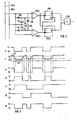
- FIG. 2 shows the circuit diagram of a receiver with two switching thresholds, the use of which may be necessary if the signals on the bus line, the wires of which are designated BL3, BL4, are severely distorted.
- the receiving circuit contains two clamping circuits, each consisting of a series circuit with a capacitor C3 or C4 and a diode D4 or D5 and between the wires BL3, BL4 of the bus line.
- a comparator VGL1, VGL2 is connected to each diode.
- the series circuit D4, C3 corresponds to the clamping circuit D2, C2 of the circuit according to FIG. 1, the comparator to the transistor T3.
- the anode of the diode D4 and the cathode of the diode D5 are connected to the positive voltage-carrying wire BL3.
- a high-resistance resistor R1 is connected in parallel with the capacitor C3.
- the potential at the non-inverting input of the comparator VGL2 is drawn via a high-resistance resistor R2, to which a diode D6 is connected in series in the exemplary embodiment, with a time constant that is large in comparison with the pulse duration, against the potential on the bus line BL3, so that signals with a different voltage swing can be detected.
- the clock inputs of bistable flip-flops FF1, FF2 are connected to the outputs of the comparators VGL1, VGL2, in such a way that the flip-flops take over the signal supplied to their preparation inputs D on negative edges.
- the preparation input D of the flip-flop FF1 is connected to the output Q of the flip-flop F F 2, the preparation input D of the flip-flop FF2 to the output Q of the flip-flop FF1.
- the outputs Q of both flip-flops are led to an exclusive OR gate EXO, at whose output the regenerated input signal appears.
- FIG. 3 shows the time diagram a the output signal of a transmitter, the diagram b the input signal of the receiver under consideration, the signals v1, v2 the output signals of its comparators VGL1 and VGL2, the diagrams f1, f2 the outputs Q of the flip-flops FF1, FF2 occurring signals and the diagram xr the output signal of the EXCLUSIVE OR element EXO.
- the positive voltage U 1 lies between the wires BL3, BL4 of the bus line.
- a small current flows through the clamping diode D4 and the resistor R1, so that a voltage of approximately 0.7 V drops at the clamping diode.
- the capacitor C3 is therefore charged to the voltage U 1 reduced by the forward voltage of the diode D4.
- the forward voltage of the diode D4 is at the input of the comparator VGL1, its output signal is therefore H, corresponding to log. "1".
- the condenser Gate C4 charged via diode D6 and resistor R2 to approximately the same value as capacitor C3, so that at the input of comparator VGL2 there is approximately the same voltage as at the input of comparator VGL1, but with different polarity. Its output signal v2 is therefore log. "0". If the transmitter, which is spatially distant from the described receiver, sends a zero signal to the bus line, the input voltage slowly drops due to the capacity of the bus line and the modules connected to it compared to the output signal of the transmitter.
- the transmitter gives a "1" signal on the bus line and the input signal rises there, a negative edge occurs in the output signal v2, which switches the flip-flop FF2.
- the output signal xr is therefore log like the output signal a of the transmitter. "1”. If the input signal e reaches the threshold voltage 51, the comparator VGL1 also switches over. However, the positive edge of its output signal v11 has no effect, so that the signal xr does not change.
- the flip-flop FF1 is only switched over with the negative flank of the signal v1 on the following negative flank of the input signal, when the threshold S1 falls below again, and the signal xr follows the signal a switched by the transmitter to the bus line.
- the threshold S2 is entered as constant for the sake of clarity. In fact, this threshold rises during times when the voltage of the input signal is greater than U2 due to the charging of the capacitor C4 the diode D6 and the resistor R2 slowly on. On the other hand, the capacitor C4 is recharged via the diode D5 during the phases of low input voltage. This means that the circuit always adapts to the lower value U2 of the input voltage. The input signals are therefore reliably detected and restored, irrespective of the position of the bus line on which the respective transmitter is located.
- the exemplary embodiment can be modified in many ways. So z. B. the diode D6 can be dispensed with and the high-resistance resistor R2 can be connected directly to the cathode of the diode D4. Furthermore, the comparators can be reversed, flip-flops can be used which switch not on the negative edges but on the positive, and the preparatory inputs of the flip-flops can be connected in a different way to the outputs of the other stage. These measures must of course be taken in a suitable combination. It is essential that there are two clamping circuits for the two input signal levels and that the current input signal level is compared with the clamping potentials and the comparison results are logically combined so that the input signal is restored.
Landscapes
- Engineering & Computer Science (AREA)
- Computer Networks & Wireless Communication (AREA)
- Signal Processing (AREA)
- Power Engineering (AREA)
- Dc Digital Transmission (AREA)
- Small-Scale Networks (AREA)
Applications Claiming Priority (2)
| Application Number | Priority Date | Filing Date | Title |
|---|---|---|---|
| DE3820561 | 1988-06-16 | ||
| DE19883820561 DE3820561A1 (de) | 1988-06-16 | 1988-06-16 | Schaltungsanordnung zum uebertragen von binaeren signalen |
Publications (2)
| Publication Number | Publication Date |
|---|---|
| EP0346572A2 true EP0346572A2 (fr) | 1989-12-20 |
| EP0346572A3 EP0346572A3 (fr) | 1991-05-08 |
Family
ID=6356707
Family Applications (1)
| Application Number | Title | Priority Date | Filing Date |
|---|---|---|---|
| EP19890104406 Withdrawn EP0346572A3 (fr) | 1988-06-16 | 1989-03-13 | Dispositif pour transmettre des signaux binaires |
Country Status (2)
| Country | Link |
|---|---|
| EP (1) | EP0346572A3 (fr) |
| DE (1) | DE3820561A1 (fr) |
Cited By (2)
| Publication number | Priority date | Publication date | Assignee | Title |
|---|---|---|---|---|
| EP0617509A3 (fr) * | 1993-03-22 | 1997-07-16 | Siemens Nixdorf Inf Syst | Alimentation en tension aux terminaison de guide d'ondes. |
| WO1998001980A1 (fr) * | 1996-07-04 | 1998-01-15 | Siemens Aktiengesellschaft | Coupleur de bus comportant un circuit emetteur commande en amplitude |
Family Cites Families (3)
| Publication number | Priority date | Publication date | Assignee | Title |
|---|---|---|---|---|
| DE2050994B2 (de) * | 1970-10-16 | 1972-04-27 | Nixdorf Computer Ag, 4790 Paderborn | Verfahren und schaltungsanordnung zur erdfreien uebertragung von gleichstromsignalen |
| DE2360376C3 (de) * | 1973-12-04 | 1978-09-21 | Siemens Ag, 1000 Berlin Und 8000 Muenchen | Schaltungsanordnung zum Empfang von Gleichstromzeichen |
| FR2443770A1 (fr) * | 1978-12-04 | 1980-07-04 | Materiel Telephonique | Recepteur pour bus ac a isolation galvanique par capacite |
-
1988
- 1988-06-16 DE DE19883820561 patent/DE3820561A1/de not_active Withdrawn
-
1989
- 1989-03-13 EP EP19890104406 patent/EP0346572A3/fr not_active Withdrawn
Cited By (4)
| Publication number | Priority date | Publication date | Assignee | Title |
|---|---|---|---|---|
| EP0617509A3 (fr) * | 1993-03-22 | 1997-07-16 | Siemens Nixdorf Inf Syst | Alimentation en tension aux terminaison de guide d'ondes. |
| WO1998001980A1 (fr) * | 1996-07-04 | 1998-01-15 | Siemens Aktiengesellschaft | Coupleur de bus comportant un circuit emetteur commande en amplitude |
| EP0822688A1 (fr) * | 1996-07-04 | 1998-02-04 | Siemens Aktiengesellschaft | Coupleur de bus avec circuit d'émission réglé en amplitude |
| US6445239B1 (en) | 1996-07-04 | 2002-09-03 | Siemens Aktiengesellschaft | Bus coupling with amplitude-controlled transmission circuit |
Also Published As
| Publication number | Publication date |
|---|---|
| DE3820561A1 (de) | 1989-12-21 |
| EP0346572A3 (fr) | 1991-05-08 |
Similar Documents
| Publication | Publication Date | Title |
|---|---|---|
| EP0191019B1 (fr) | Installation pour le transfert de donnees binaires entre un support d'information mobile et une station fixe | |
| DD150824A5 (de) | Vorrichtung zur uebertragung von informationen auf einer wechselstromleitung | |
| DE1952796A1 (de) | Schaltungsanordnung zur verlustarmen Stabilisierung einer Eingangswechselspannung | |
| DE1130922B (de) | Vorrichtung zur UEberwachung des oberen und unteren Grenzwertes eines Gleichspannungspegels | |
| DE2156873C3 (de) | Verfahren und Vorrichtung zur Fernsteuerung mittels den einzelnen Befehlen zugeordneten Impulsbildern | |
| DE2903860A1 (de) | Einrichtung zur gleichstromversorgung eines verbrauchers und zur gleichzeitigen informationsuebertragung ueber ein aderpaar | |
| DE19532677B4 (de) | Überwachungsschaltung für wenigstens eine Versorgungsspannung | |
| EP0014328B1 (fr) | Circuit d'occupation pour le fil "entrant" c dans un dispositif de télécommunication | |
| DE2130916B2 (de) | Übertragungsschaltung für digitale Signale | |
| DE2942440A1 (de) | Geraet zur ueberwachung des linienstromes in einer telefonleitung | |
| DE3618500A1 (de) | Schaltungsanordnung zum verpolschutz | |
| WO1990008437A2 (fr) | Raccordement de postes a des bus | |
| DE2050994B2 (de) | Verfahren und schaltungsanordnung zur erdfreien uebertragung von gleichstromsignalen | |
| DE3820561A1 (de) | Schaltungsanordnung zum uebertragen von binaeren signalen | |
| DE3010535C2 (de) | Regenerator für digitale Signale | |
| EP0569883A2 (fr) | Constitution des circuits pour limitation du courant lors de la fermeture du circuit à ensemble électronique | |
| DE3117927C2 (de) | Anordnung zur Erkennung der längsten von in digitalen Signalen periodisch enthaltenen Folgen von Nullzeichen | |
| DE3020354A1 (de) | Elektronischer sender fuer gleichstromtelegraphiesysteme | |
| EP0499869B1 (fr) | Circuit pour génération de tension alternative | |
| DE2719223B1 (de) | Anordnung zum Umsetzen von Alarmsignalen zwischen einem digitalen Nachrichtenuebertragungssystem und einer zentralen Betriebsueberwachung | |
| EP0582890B1 (fr) | Arrangement de circuit | |
| DE4014267A1 (de) | Schaltungsanordnung zur erkennung eines in einer elektrischen leitung fliessenden stroms | |
| DE1128466B (de) | Eingangsschaltung zur Steuerung eines bistabilen Schaltkreises | |
| DE3910685A1 (de) | Schaltungsanordnung zur bedaempfung eines sperrwandlers | |
| DE3725882C2 (de) | Verfahren und Vorrichtung zur Übertragung von Signalen einer Fernsprecheinrichtung |
Legal Events
| Date | Code | Title | Description |
|---|---|---|---|
| PUAI | Public reference made under article 153(3) epc to a published international application that has entered the european phase |
Free format text: ORIGINAL CODE: 0009012 |
|
| AK | Designated contracting states |
Kind code of ref document: A2 Designated state(s): BE DE FR GB NL SE |
|
| 17P | Request for examination filed |
Effective date: 19901205 |
|
| PUAL | Search report despatched |
Free format text: ORIGINAL CODE: 0009013 |
|
| AK | Designated contracting states |
Kind code of ref document: A3 Designated state(s): BE DE FR GB NL SE |
|
| STAA | Information on the status of an ep patent application or granted ep patent |
Free format text: STATUS: THE APPLICATION IS DEEMED TO BE WITHDRAWN |
|
| 18D | Application deemed to be withdrawn |
Effective date: 19911109 |