EP0346776A1 - Circuit décodeur pour code à trois parties - Google Patents
Circuit décodeur pour code à trois parties Download PDFInfo
- Publication number
- EP0346776A1 EP0346776A1 EP89110495A EP89110495A EP0346776A1 EP 0346776 A1 EP0346776 A1 EP 0346776A1 EP 89110495 A EP89110495 A EP 89110495A EP 89110495 A EP89110495 A EP 89110495A EP 0346776 A1 EP0346776 A1 EP 0346776A1
- Authority
- EP
- European Patent Office
- Prior art keywords
- signal
- bitcell
- clock
- data
- time
- Prior art date
- Legal status (The legal status is an assumption and is not a legal conclusion. Google has not performed a legal analysis and makes no representation as to the accuracy of the status listed.)
- Withdrawn
Links
- 230000007704 transition Effects 0.000 claims description 39
- 238000000034 method Methods 0.000 claims description 17
- 239000003990 capacitor Substances 0.000 claims description 9
- 230000000694 effects Effects 0.000 description 3
- 230000001939 inductive effect Effects 0.000 description 2
- 230000001133 acceleration Effects 0.000 description 1
- 230000001419 dependent effect Effects 0.000 description 1
- 230000004069 differentiation Effects 0.000 description 1
- 238000004146 energy storage Methods 0.000 description 1
- 230000000977 initiatory effect Effects 0.000 description 1
- 230000010354 integration Effects 0.000 description 1
- 230000003287 optical effect Effects 0.000 description 1
- 238000004321 preservation Methods 0.000 description 1
Images
Classifications
-
- G—PHYSICS
- G11—INFORMATION STORAGE
- G11B—INFORMATION STORAGE BASED ON RELATIVE MOVEMENT BETWEEN RECORD CARRIER AND TRANSDUCER
- G11B20/00—Signal processing not specific to the method of recording or reproducing; Circuits therefor
- G11B20/10—Digital recording or reproducing
- G11B20/14—Digital recording or reproducing using self-clocking codes
-
- H—ELECTRICITY
- H03—ELECTRONIC CIRCUITRY
- H03M—CODING; DECODING; CODE CONVERSION IN GENERAL
- H03M5/00—Conversion of the form of the representation of individual digits
- H03M5/02—Conversion to or from representation by pulses
- H03M5/04—Conversion to or from representation by pulses the pulses having two levels
- H03M5/06—Code representation, e.g. transition, for a given bit cell depending only on the information in that bit cell
- H03M5/12—Biphase level code, e.g. split phase code, Manchester code; Biphase space or mark code, e.g. double frequency code
Definitions
- This invention relates to electrical circuits suitable for decoding an encoded binary data stream.
- a novel method for modulating a binary data stream into a code format suitable for encoding and decoding e.g., magnetic or optical information is disclosed in the above-cited Application Ser. No. 206,646 to Wash.
- the novel method features self-clocking, velocity insensitive encoding and decoding.
- the Wash disclosure states that preferred electrical circuits that may be employed for realizing the decoding scheme set forth in that disclosure are provided in the present application.
- This application therefore, provides novel electrical circuits that may be advantageously employed, for example, in decoding an encoded binary data stream.
- the novel electrical circuits include analog circuitry, and are preferably employed to decode magnetic information or data that has been encoded in a three-part-cell code format in accordance with the Wash disclosure.
- the novel electrical circuits decode the encoded data, and preserve the self-clocking, velocity insensitive features of the novel method.
- the invention provides an electrical circuit suitable for decoding a binary data stream that has been encoded in a sequential bitcell code format, the encoding resulting in an encoded signal waveform that carries clock information and data information, which electrical circuit comprises:
- the novel electrical circuit as defined preserves the self-clocking, velocity insensitive features of the Wash method for encoding the decoding information. This preservation factor is provided by the electrical circuit in the following way.
- the time t i between two adjacent clock transitions of a first bitcell may differ from the time t j between two adjacent clock transitions of a second bitcell. This is a consequence of the information transfer rate being dependent on unpredictable and variable transfer rate velocities and accelerations.
- the present electrical circuit accommodates such unpredictable and variable transfer rates by way of e.g., the clock signal integrator, which integrates over a variable path length t0 to t1, the variable path length therefore accommodating the variable times t i , t j .
- the circuit integrator means generates the parameter which is a measure of an instantaneous bitcell half way point.
- the circuit integrator means also acts in cooperation with the other elements, to the end of accommodating the variable sequential bitcell times, t i , t j .
- the comparer means acts in cooperation with the clock signal integrator and the circuit integrator means, by acting upon the varying time location data signal in coordination with the variable sequential bitcell times, t i , t j .
- the separator means separates the encoded signal waveform in accordance with the method of encoding, and subsequent reading of the encoded signal waveform.
- the separator means preferably comprises:
- An encoded signal waveform preferably encodes data information by assigning it a positive polarity, and on the other hand, encodes clock information by assigning it a negative polarity.
- the separator means accordingly, preferably separates the clock information from the data information by detecting waveform peaks i.e., positive pulses or data information, the waveform valleys i.e., negative pulses or clock information.
- the separator means operates on a succession of bitcells, and preferably generates an output pulse train that represents the sequential clock signals, and an output pulse train that represents the sequential data signals.
- the clock signal integrator preferably comprises a capacitor circuit. Energy stored and released by the capacitor circuit for each bitcell can provide a measure of the integrated output signal, and a measure of the duration t i of each bitcell.
- the circuit integrator means preferably integrates the integrated output signal, in order to provide a time average for each bitcell.
- the comparer means preferably comprises a computer, although it may comprise e.g., a shift register circuit, or flip-flop logic circuit.
- the invention provides an electrical circuit suitable for decoding a binary data stream that has been encoded by a three-part code method, which method comprises:
- the novel method comprises
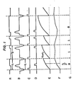
- FIG. 1a shows a sequence of bitcells. Each bitcell is defined by a variable time t i between two adjacent clock transition pulses. Within each bitcell, a data 0 bit or a data 1 bit has been encoded in accordance with the ratio as defined. For illustration purposes, a data 0 bit has been encoded by the ratio and a data 1 bit has been encoded by the ratio
- the method of decoding the encoded waveform of magnetic systems first requires the employment of a magnetic reader.
- the magnetic reader may provide a time derivative encoded waveform of that shown in FIG. 1A.
- This time derivative encoded waveform is shown in FIG. 1B.
- FIG. 1B shows an analog encoded waveform, comprising (albeit in a different form from FIG. 1A) the clock information mixed in with the data information.
- FIG. 1B shows that each bitcell is defined by the variable time t i , and that the clock information comprises negative pulses or valleys, and that the data information comprises positive pulses or peaks.
- the encoded waveform of FIG. 1B may be decoded by the step of determining the time between the first clock transition and the data transition, and comparing this time to the variable bitcell time t i .
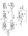
- Preferred circuitry for realizing this step is shown in FIG. 2.
- FIG. 2 shows an electrical circuit 10 suitable for decoding the encoded signal waveform that carries clock information and data information i.e., the waveform of FIG. 1B.
- the structure of the electric circuit 10 is as follows.
- the electrical circuit 10 comprises a separator means 12 that receives the encoded signal waveform along a line 14.
- the separator means 12 comprises a negative peak detector 16, and a positive peak detector 18 connected in parallel with the negative peak detector 16.
- the positive peak detector 18 is connected in series along a line 20 to a comparer means 22.
- the negative peak detector 16 on the other hand, is connected in series along a line 24 to a clock signal integrator 26.
- the clock signal integrator 26 in turn, is connected in series along a line 28, to a circuit integrator means 30, and to the comparer means 22 along a line 32.
- the circuit integrator means 30 is connected in series to the comparer means 22 along a line 34.
- FIG. 2 electrical circuit 10 The operation of the FIG. 2 electrical circuit 10 is now explained, with continued reference to the signal waveforms shown in FIG. 1, and with subsequent reference to FIGS. 3 and 4.
- the encoded waveform comprising clock information mixed in with the data information (FIG. 1B), is provided as an input along the line 14 to the separator means 12.
- the separator means 12 provides an output clock signal (CS) and an output data signal, for each of a succession of bitcells.
- the separator means 12 accomplishes this by way of the negative peak detector 16, that detects the encoded signal waveform for clock-information, and the positive peak detector 18, that detects the encoded signal waveform for data information.
- the negative peak detector 16 detects the encoded signal waveform for valleys, or negative pulses
- the positive peak detector 18 detects the encoded signal waveform for peaks, or positive pulses.
- the detector 16 outputs a clock signal (CS) pulse train (see FIG. 1C) for input along the line 24 to the clock signal integrator 26.
- the detector 18, on the other hand, outputs a data signal pulse train (see FIG. 1D) for input to the comparer means 22 along the line 20.
- FIG. 1E shows sequential expotential waveforms, where any one expotential waveform corresponds to a bitcell having a variable time t i .
- t i is defined as the time of the end of a bitcell (t1), minus the time of the beginning of the bitcell (t0).
- the clock integrator 26 comprises a capacitor circuit 36.
- the capacitor circuit 36 comprises a capacitor C connected to ground, and driven by a current source (IS).
- IS current source
- V i variable voltage potentials
- the variable voltage potentials V i are shown in FIG. 1E.
- the determinant for initiating and concluding capacitor circuit energy storage and release is the advent of sequential clock signal pulses.
- the clock integrator 26 accordingly, generates an integrated output signal that indicates the time duration t i for each bitcell.
- This integrated output signal is inputted to the comparer means 22 along the line 32.
- the clock integrator 26 outputs the integrated output signal, for input to the circuit integrator means 30 along the line 28.
- the circuit integrator means 30 functions to integrate the Fig. 1E integrated output signal, to the effect of generating the parameter for each bitcell, as shown in FIG. 1F.
- the importance of the parameter and hence of the circuit integrator means 30, is that it provides an indication of the half way point of each bitcell.
- the circuit integrator means 30 uses the parameter as a projected estimate of the bitcell time of a sequential bitcell.
- the comparer means 22 inputs the data signal pulse train (Fig. 1D) along the line 20, inputs the parameter along the line 34, and also inputs the integrated output signal along the line 32.
- the comparer means 22 compares the data signal for each bitcell, with the previous bitcell's parameter
- the comparer means 22 assigns a decoded signal a first valuation if the data signal is less that and a second valuation if the data signal is greater than
- FIG. 1G shows decoded information for sequential bitcells.
- sequential bitcells may be demarked by comparing FIG. 1G to the FIG. 1C clock signal pulse train.
- Each FIG. 1G bitcell, according to the Wash method is defined by a variable time t i .
- This time, t i is known by the comparer means 22, since it knows the parameter for each previous bitcell.
- the comparer means 22, in the same way, knows the time of the beginning of a bitcell t o , the time of the end of that bitcell, t1 and the variable time t i defined by that bitcell.
- the comparer means 22 also receives a data signal along the line 20.
- the comparer means 22 accordingly, at the time of the receipt of the data signal, assigns the decoded signal a first valuation if the data signal is less than the known parameter and a second valuation if the data signal is greater than
- the comparer means 22 accordingly, provides information that is a decoding of the data contained in the FIG. 1A waveform, namely, the FIG. 1G.
- FIG. 1G a logic transition initiated by the data signal, sensed by the comparer means 22, occurring before signifies a data 0 bit.
- the comparer means 22 comprises a computer.
- a suitable program run by the computer to realize the operation of the comparer means 22, is listed below.
- A/D analog-to-digital converters
- the A/D outputs are connected to a Port A and to a Port B in the computer.
- Port A is dedicated to the integrated output signal (IOS) provided on line 32, while the Port B is dedicated to the output of the circuit integrator means 30 on line 34.
- IOS integrated output signal
- the data signal pulse train on line 20 is also supplied to the computer, by way of a Port C.
- a suitable program, written in BASIC, is now listed:
- the output in the program example is a variable named "BIT". If the data signal pulse occurs in the second half of a bitcell, the variable named "BIT" is assigned a data 1. Similarly, if the data signal pulse occurs in the first half of a bitcell, the variable named "BIT" is assigned a data 0.
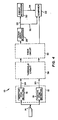
- FIG. 4 shows the electrical circuit 10 of FIG. 2, as well as a threshold circuit 38 and a timer circuit 40.
- the threshold circuit 38 is connected, as shown, between the separator means 12 and the clock signal integrator 26.
- the threshold circuit 38 is preferably employed e.g., to suppress noise embedded in the FIG. 1B waveform, to minimize the effects of amplitude changes in the FIG. 1B waveform, and/or to provide a digital variant of the FIG. 1B waveform.
- the timer circuit 40 connected as shown between the threshold circuit 38, the clock signal integrator 26 and the data comparer means 22, preferably is employed to address the following problem.
- the electrical circuit 10 may input sequential bitcells of unacceptably long duration. Or, a sequential bitcell string may simply come to an end. In either case, the timer circuit 40 may be used to disable further input to the clock signal integrator 26 and the comparer means 22 after a preselected interval.
Landscapes
- Engineering & Computer Science (AREA)
- Theoretical Computer Science (AREA)
- Signal Processing (AREA)
- Synchronisation In Digital Transmission Systems (AREA)
- Dc Digital Transmission (AREA)
- Compression, Expansion, Code Conversion, And Decoders (AREA)
Applications Claiming Priority (2)
| Application Number | Priority Date | Filing Date | Title |
|---|---|---|---|
| US20640788A | 1988-06-14 | 1988-06-14 | |
| US206407 | 1988-06-14 |
Publications (1)
| Publication Number | Publication Date |
|---|---|
| EP0346776A1 true EP0346776A1 (fr) | 1989-12-20 |
Family
ID=22766229
Family Applications (1)
| Application Number | Title | Priority Date | Filing Date |
|---|---|---|---|
| EP89110495A Withdrawn EP0346776A1 (fr) | 1988-06-14 | 1989-06-09 | Circuit décodeur pour code à trois parties |
Country Status (3)
| Country | Link |
|---|---|
| EP (1) | EP0346776A1 (fr) |
| KR (1) | KR900702528A (fr) |
| WO (1) | WO1989012894A1 (fr) |
Cited By (1)
| Publication number | Priority date | Publication date | Assignee | Title |
|---|---|---|---|---|
| US9650666B2 (en) | 2001-06-30 | 2017-05-16 | Enzo Biochem, Inc. | Processes for detecting or quantifying nucleic acids using an array of fixed or immobilized nucleic acids |
Families Citing this family (2)
| Publication number | Priority date | Publication date | Assignee | Title |
|---|---|---|---|---|
| KR910007815B1 (ko) * | 1988-12-31 | 1991-10-02 | 삼성전자 주식회사 | 바이패이즈 엔코딩 데이터의 디코딩방법 |
| DK0489819T3 (da) * | 1989-08-31 | 1993-08-30 | Eastman Kodak Co | Forbedret dekodningskredsløb |
Citations (4)
| Publication number | Priority date | Publication date | Assignee | Title |
|---|---|---|---|---|
| US3475062A (en) * | 1966-05-11 | 1969-10-28 | Westinghouse Electric Corp | Time discriminator |
| US4037257A (en) * | 1976-02-02 | 1977-07-19 | Xerox Corporation | Data clock separator with missing clock detect |
| GB1484290A (en) * | 1974-01-23 | 1977-09-01 | Ibm | Digital data detection circuits |
| GB1542398A (en) * | 1976-05-24 | 1979-03-21 | Secr Defence | Recording data |
-
1989
- 1989-06-08 WO PCT/US1989/002476 patent/WO1989012894A1/fr not_active Ceased
- 1989-06-08 KR KR1019900700298A patent/KR900702528A/ko not_active Withdrawn
- 1989-06-09 EP EP89110495A patent/EP0346776A1/fr not_active Withdrawn
Patent Citations (4)
| Publication number | Priority date | Publication date | Assignee | Title |
|---|---|---|---|---|
| US3475062A (en) * | 1966-05-11 | 1969-10-28 | Westinghouse Electric Corp | Time discriminator |
| GB1484290A (en) * | 1974-01-23 | 1977-09-01 | Ibm | Digital data detection circuits |
| US4037257A (en) * | 1976-02-02 | 1977-07-19 | Xerox Corporation | Data clock separator with missing clock detect |
| GB1542398A (en) * | 1976-05-24 | 1979-03-21 | Secr Defence | Recording data |
Cited By (1)
| Publication number | Priority date | Publication date | Assignee | Title |
|---|---|---|---|---|
| US9650666B2 (en) | 2001-06-30 | 2017-05-16 | Enzo Biochem, Inc. | Processes for detecting or quantifying nucleic acids using an array of fixed or immobilized nucleic acids |
Also Published As
| Publication number | Publication date |
|---|---|
| WO1989012894A1 (fr) | 1989-12-28 |
| KR900702528A (ko) | 1990-12-07 |
Similar Documents
| Publication | Publication Date | Title |
|---|---|---|
| CA1059636A (fr) | Appareil et methode de codage par modulation modifiee de zeros | |
| US4506252A (en) | Ternary data encoding system | |
| JPS57176866A (en) | Encoder of binary signal | |
| EP0199088B1 (fr) | Méthode et appareil pour modifier un code à longueur de course limitée | |
| EP0122027A1 (fr) | Système de codage-décodage à longueur de mot variable | |
| JPS57195308A (en) | Block coding method | |
| MY103398A (en) | Method and apparatus for demodulating a biphase signal | |
| US4232388A (en) | Method and means for encoding and decoding digital data | |
| EP0346774A1 (fr) | Circuit décodeur pour code à trois parties | |
| US4307381A (en) | Method and means for encoding and decoding digital data | |
| CA2064320A1 (fr) | Circuit d'extraction de signaux d'horloge a comparaison du niveau de stockage de la memoire avec des seuils haut, moyen et bas | |
| US4204199A (en) | Method and means for encoding and decoding digital data | |
| US4964139A (en) | Multi-purpose circuit for decoding binary information | |
| EP0346776A1 (fr) | Circuit décodeur pour code à trois parties | |
| US4567604A (en) | Biphase signal receiver | |
| ES460639A1 (es) | Metodo y su correspondiente aparato para codificar una in- formacion binaria. | |
| US5025328A (en) | Circuit for decoding binary information | |
| US4063291A (en) | Apparatus and method for encoding and decoding digital information | |
| EP0064406A1 (fr) | Codage de données binaires | |
| SU1531154A1 (ru) | Устройство дл преобразовани двоичной последовательности в фазомодулированный сигнал | |
| SU486372A1 (ru) | Способ магнитной записи и считывани цифровой информации | |
| JPS634270B2 (fr) | ||
| EP0489819B1 (fr) | Circuit decodeur ameliore | |
| JP2673068B2 (ja) | レート2/5(2、18、2)符号を使用する2進データの符号化および復号の方法及び装置 | |
| SU1027766A1 (ru) | Устройство дл магнитной записи цифровой информации без посто нной составл ющей |
Legal Events
| Date | Code | Title | Description |
|---|---|---|---|
| PUAI | Public reference made under article 153(3) epc to a published international application that has entered the european phase |
Free format text: ORIGINAL CODE: 0009012 |
|
| AK | Designated contracting states |
Kind code of ref document: A1 Designated state(s): ES |
|
| STAA | Information on the status of an ep patent application or granted ep patent |
Free format text: STATUS: THE APPLICATION IS DEEMED TO BE WITHDRAWN |
|
| 18D | Application deemed to be withdrawn |
Effective date: 19900621 |