EP0349732B1 - Amplificateur de puissance - Google Patents
Amplificateur de puissance Download PDFInfo
- Publication number
- EP0349732B1 EP0349732B1 EP89108457A EP89108457A EP0349732B1 EP 0349732 B1 EP0349732 B1 EP 0349732B1 EP 89108457 A EP89108457 A EP 89108457A EP 89108457 A EP89108457 A EP 89108457A EP 0349732 B1 EP0349732 B1 EP 0349732B1
- Authority
- EP
- European Patent Office
- Prior art keywords
- series
- filter
- switching
- power amplifier
- mains
- Prior art date
- Legal status (The legal status is an assumption and is not a legal conclusion. Google has not performed a legal analysis and makes no representation as to the accuracy of the status listed.)
- Expired - Lifetime
Links
- 238000004804 winding Methods 0.000 claims description 46
- 239000003990 capacitor Substances 0.000 claims description 27
- 101100073352 Streptomyces halstedii sch1 gene Proteins 0.000 claims description 20
- 101100073357 Streptomyces halstedii sch2 gene Proteins 0.000 claims description 20
- 238000001208 nuclear magnetic resonance pulse sequence Methods 0.000 claims description 17
- 238000010276 construction Methods 0.000 claims description 10
- 230000005540 biological transmission Effects 0.000 claims description 7
- 101100191136 Arabidopsis thaliana PCMP-A2 gene Proteins 0.000 claims description 6
- 101100054666 Streptomyces halstedii sch3 gene Proteins 0.000 claims description 5
- 101100276531 Streptomyces halstedii sch4 gene Proteins 0.000 claims description 5
- 239000004065 semiconductor Substances 0.000 claims description 5
- 230000003068 static effect Effects 0.000 claims description 5
- 230000006698 induction Effects 0.000 claims description 4
- 230000005669 field effect Effects 0.000 claims description 2
- 238000009434 installation Methods 0.000 claims description 2
- 238000004519 manufacturing process Methods 0.000 claims description 2
- 239000002245 particle Substances 0.000 claims description 2
- 239000004020 conductor Substances 0.000 claims 2
- 238000006073 displacement reaction Methods 0.000 claims 2
- 230000003287 optical effect Effects 0.000 claims 2
- 238000012216 screening Methods 0.000 claims 1
- 230000008901 benefit Effects 0.000 description 8
- 238000010586 diagram Methods 0.000 description 6
- 238000002955 isolation Methods 0.000 description 6
- 238000005070 sampling Methods 0.000 description 6
- 230000010355 oscillation Effects 0.000 description 5
- 238000011161 development Methods 0.000 description 4
- 230000018109 developmental process Effects 0.000 description 4
- 230000010363 phase shift Effects 0.000 description 4
- 230000009467 reduction Effects 0.000 description 4
- 230000003321 amplification Effects 0.000 description 3
- 230000007423 decrease Effects 0.000 description 3
- 238000003199 nucleic acid amplification method Methods 0.000 description 3
- XEEYBQQBJWHFJM-UHFFFAOYSA-N Iron Chemical group [Fe] XEEYBQQBJWHFJM-UHFFFAOYSA-N 0.000 description 2
- 238000005516 engineering process Methods 0.000 description 2
- 230000006872 improvement Effects 0.000 description 2
- 239000011810 insulating material Substances 0.000 description 2
- 230000010354 integration Effects 0.000 description 2
- JMYNPQVCVQVODQ-OWOJBTEDSA-N 1,3-dichloro-5-[(e)-2-(4-chlorophenyl)ethenyl]benzene Chemical compound C1=CC(Cl)=CC=C1\C=C\C1=CC(Cl)=CC(Cl)=C1 JMYNPQVCVQVODQ-OWOJBTEDSA-N 0.000 description 1
- 241001076195 Lampsilis ovata Species 0.000 description 1
- 230000015572 biosynthetic process Effects 0.000 description 1
- 230000008859 change Effects 0.000 description 1
- 238000013016 damping Methods 0.000 description 1
- 238000013461 design Methods 0.000 description 1
- 230000006866 deterioration Effects 0.000 description 1
- 238000007599 discharging Methods 0.000 description 1
- 230000000694 effects Effects 0.000 description 1
- 230000008030 elimination Effects 0.000 description 1
- 238000003379 elimination reaction Methods 0.000 description 1
- 239000000835 fiber Substances 0.000 description 1
- 238000009499 grossing Methods 0.000 description 1
- 238000000034 method Methods 0.000 description 1
- 230000004048 modification Effects 0.000 description 1
- 238000012986 modification Methods 0.000 description 1
- 238000005457 optimization Methods 0.000 description 1
- 101150094737 pdm2 gene Proteins 0.000 description 1
- 230000008569 process Effects 0.000 description 1
- 239000011347 resin Substances 0.000 description 1
- 229920005989 resin Polymers 0.000 description 1
- 239000007787 solid Substances 0.000 description 1
- 230000003595 spectral effect Effects 0.000 description 1
- 238000001228 spectrum Methods 0.000 description 1
- 238000003860 storage Methods 0.000 description 1
- 230000001360 synchronised effect Effects 0.000 description 1
- 238000012549 training Methods 0.000 description 1
- 238000012546 transfer Methods 0.000 description 1
- 238000011144 upstream manufacturing Methods 0.000 description 1
Images




Classifications
-
- H—ELECTRICITY
- H03—ELECTRONIC CIRCUITRY
- H03F—AMPLIFIERS
- H03F3/00—Amplifiers with only discharge tubes or only semiconductor devices as amplifying elements
- H03F3/20—Power amplifiers, e.g. Class B amplifiers, Class C amplifiers
- H03F3/21—Power amplifiers, e.g. Class B amplifiers, Class C amplifiers with semiconductor devices only
- H03F3/217—Class D power amplifiers; Switching amplifiers
- H03F3/2178—Class D power amplifiers; Switching amplifiers using more than one switch or switching amplifier in parallel or in series
Definitions
- the invention relates to a power amplifier according to the preamble of patent claim 1.
- Amplifiers of this type are generally used for the power amplification of analog input signals, in particular of the low-frequency or audio frequency range at a high voltage level, and are characterized in particular by a high degree of efficiency and high reproduction quality, ie by a low distortion of the amplifier output signal even in the range from voltages up to 30-50 kV out. They are preferred as modulation amplifiers for transmitters and here in particular for amplitude-modulated high-performance radio transmitters used in the long, medium and short wave range with an anode-modulated RF power amplifier tube, but also as a high-voltage direct current supply, especially for the power supply of magnets in particle accelerator systems. Other applications such as loudspeaker systems are also possible.
- a power amplifier known from EP-A1-0 025 234 consists of N switching amplifiers connected in series on the output side and connected on the primary side and a downstream low-pass filter.
- the N switching amplifiers are combined to form N / 2 pairs, each of which is controlled by two pulse-duration-modulated pulse trains that are 180 ° out of phase with each other, while the phase shift between the individual pulse train pairs is 360 ° / N.
- Pairing is necessary in this known amplifier, since otherwise the magnetic reversal of the isolating transformers in the individual switching amplifiers, the use of which is absolutely necessary for the electrical isolation of the supply voltage input of the respective switching amplifier from its output, affects the pulse duty factor of the individual pulse trains, i.e. would limit the ratio of the pulse duration to the period of the switching oscillation to about 0.5 or 50% modulation.
- the downstream low-pass filter is dimensioned in its upper limit frequency so that the amplified and essentially undistorted input signal is present at its output.
- the filter effort in such a case "Multi-phase" pulse duration modulated amplifier because of the resulting higher sampling rate ia much lower than with a comparable conventional "single phase” pulse duration modulated amplifier (in which the individual pulse trains are not phase-shifted against each other), since the sum signal of the switching amplifier connected in series before the low-pass filter in In the first case, the amplified analog input signal at the output of the low-pass filter is approximated to a first approximation, ie contains it completely, but is overlaid with parts of the switching oscillation (see also FIG. 3c).
- the solution in this regard is achieved with this amplifier through the use of amplifier stages connected on the secondary side, which are connected in series on the output side.
- the switches on the secondary side if controlled with pulse-width modulated pulses, can cause underscore distortion as the pulse duty factor decreases. These underscore distortions are due to the discharge time of the switch output capacitors.
- a major cause of the surprisingly low efficiency of the known power amplifiers in practice is the power loss in the design capacitances of the network transformers used in the switching amplifiers due to the high sampling or switching frequency.
- the shielding capacitances CT between the shielding and secondary windings of the mains transformer in the case of mains transformers without shielding, the winding capacitances between the primary and secondary windings of the transformer) that are responsible for the high power loss in the transformers.
- the cross capacitances CQ between adjacent secondary windings can also contribute significantly to these losses.
- the object on which the invention is based is to create a power amplifier which, with high efficiency and high reproduction quality, manages with a lower transformer expenditure in order to realize an amplification of the analog input signal, in particular at a high voltage level.
- switching amplifiers connected on the secondary side are used, inter alia, as switching amplifiers, since in these switching amplifiers the electrical isolation of the switching amplifier output from the supply voltage input, that is to say the mains connection, is already carried out by the mains transformer and the use of special isolating transformers is therefore not necessary, so that a limitation to one Even number of switching amplifiers is eliminated in the solution according to the invention and the individual switching amplifiers can also be driven up to 100%.
- the phase shift between two temporally directly successive pulse sequences is advantageously 360 ° / N, where N is the number of switching amplifier modules used.
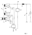
- the power amplifier in FIG. 1 consists of N preferably similar switching amplifiers V1-VN connected on the secondary side, which are connected in series on the output side and which are followed by a low-pass filter FL and FC, which is dimensioned in its upper limit frequency so that the amplified and essentially undistorted input signal is present at the amplifier output.
- the load is exemplified by an ohmic resistor R.
- a (for example single-phase) network transformer TR which has a primary winding 2 connected to a supply network (not shown) and a number of secondary windings 41-4N corresponding to the number of switching amplifiers V1-VN, the switching amplifiers V1-VN with their supply voltage inputs are connected to the corresponding secondary windings 41-4N of the mains transformer TR.
- the transformer TR is additionally provided with a grounding shield 3, via which the capacitive currents caused by the RF signal to be transmitted and, when switching amplifiers without integrated low-pass filters are not used according to the invention, the additional capacitive currents caused by the secondary switching of the DC voltages, can be derived to ground.
- the switching amplifiers V1-VN are with their control inputs via separate control lines ST1-STN with a common one Control circuit ST connected, which can be implemented for example as a digital computer circuit or in analog technology.
- a measuring point MP is provided, at which the output voltage of the switching amplifier part is tapped and fed to the control circuit ST as a feedback signal RS via a voltage divider SPT.
- pulse-duration-modulated pulse trains for controlling the individual switching amplifiers V1-VN are generated as a function of the input signal NF present on the input side and corrected by the feedback signal, and are transmitted to the assigned switching amplifier stages V1-VN via the individual control lines ST1-STN.
- the individual pulse sequences are phase-shifted with respect to one another, the phase shift between two successive pulse sequences being advantageously 360 ° / N.
- the individual control lines ST1-STN are advantageously implemented at least in sections in the form of light guide cables.
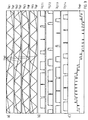
- the pulse duration modulated and also phase shifted pulse sequences at the outputs of the individual switching amplifiers are added up due to the series connection, the summation signal already approximating the amplified input signal in a first approximation, as shown in FIG. 3c is shown on the basis of a summation signal U MP, which is formed, for example, from four switching pulse sequences U ST1 -U ST4 , each phase-shifted by 90 ° with respect to one another, whose switching pulse durations are in each case proportional to the corresponding amplitude values of an exemplary sinusoidal input signal U NF .
- the summation signal U MP is subjected to a further smoothing, ie the remaining parts of the switching oscillation and its harmonics are blocked (strongly damped in practice), so that the amplified input signal is essentially undistorted at the output of the filter .
- the feedback of part of the summation signal into the input circuit of the amplifier compensates (static or dynamic) inequalities in the individual switching amplifier stages V1-VN, which would further distort the output signal without this compensation, which would result when the power amplifier according to the invention is used as a modulation amplifier in a transmitter would appear in the frequency spectrum either as discrete spectral lines or in the form of noise the own message channel or in the form of excessive edge transmissions, which would disturb the adjacent channels.
- FIG. 2 is an advantageous embodiment of the control circuit ST of the power amplifier according to FIG. 1 shown.
- each of the switching amplifiers V1-VN is assigned a separate pulse duration modulator PDM1-PDMN, which can be constructed using digital or analog technology and which generates the pulse sequence required to control the switching amplifier V1-VN assigned to it and this via the associated control line ST1 -STN to the switching amplifier V1-VN.
- PDM1-PDMN pulse duration modulator
- the individual pulse duration modulators PDM1-PDMN are connected with their reference inputs via separate second transmission lines K1-KN to a common reference oscillator stage ROS, which generates the reference or switching oscillation required for the formation of the pulse duration-modulated pulse sequences with the phase relationship required for the respective switching amplifier V1-VN.
- the pulse duration modulators PDM1-PDM4 are connected via separate first transmission lines LK1-LKN to a common modulator pre-stage VM, which processes the input signal NF to be amplified for the pulse duration modulators PDM1-PDMN.
- either the control lines ST1-STN or, alternatively, both the first and the second transmission lines LK1-LKN or K1-KN are advantageously implemented at least in sections with light guide cables.
- FIG. 3 shows an example of four switching amplifiers V1-V4 connected in series with an analog control circuit according to FIG. 2 typical voltage-time curves of individual signals.
- FIG. 3a shows the exemplary sinusoidal input signal voltage U NF that is used in the four pulse duration modulators PDM1 PDM2 is compared with, for example triangular reference or control voltages U K1 -U CN, with the individual reference voltages U K1 -U CN are respectively mutually phase-shifted by 90 °.
- the corresponding pulse duration modulator In the times when the input signal voltage U NF is greater than or equal to the respective reference voltages U K1 -U KN , the corresponding pulse duration modulator generates a positive output pulse.
- the resulting output pulse sequences U ST1 -U ST4 are shown in FIG. 3b shown. They are used to control the corresponding switching amplifiers V1-V4, at the outputs of which are generated synchronously with the control pulse sequences U ST1 -U ST4 switching pulse sequences which are summed up to a summation signal U MP , as shown in FIG. 3c shows.
- the comparison of the input signal NF with a reference signal is carried out after digitization on the input side, in that the FIG. 3 triangularly selected reference voltages U K1 -U KN are replaced by synchronously connected counters and the comparison of the input signal is carried out digitally.
- the counters can be implemented, for example, as discrete integrated circuits or preferably with the aid of a signal processor, the large number of counters being implemented using an appropriate algorithm.
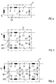
- FIGS. 4-5 show two previously proposed embodiments of switching amplifiers V which are connected on the secondary side and which are designed as examples and are also advantageously implemented in the power amplifier according to FIG. 1 can be used.
- the basic circuit known from DE-A1-30 44 956 in FIG. 4 consists of a rectifier diode G, a filter inductor L, a filter capacitor C, which together with a power transformer, of which only the secondary winding 4 is shown, form a DC power supply unit UB, which can be switched on and off by a switch S and which is switched off State is bridged by a free-wheeling diode D.
- the switch S is controlled by the pulse sequence generated in the control circuit (ST not shown in FIG. 1 or 2).
- the circuit known from EP-A1-0 066 904 according to FIG. 5 consists of a double power supply unit, which is composed of two DC power supply units UB1 and UB2 connected in series and connected to a common secondary winding 4 and which can be switched on and off via switches S1 and S2 and, when switched off, by the two freewheeling diodes connected in series D1 and D2 is bridged.
- the switches S1 and S2 can be controlled independently of one another, so that one DC voltage power supply unit UB1 can be switched on and off independently of the other DC voltage power supply unit UB2.
- the switches S1 and S2 can thus either be controlled with the same pulse train or alternatively by two pulse trains which are phase-shifted with respect to one another.
- FIG. 6 shows the basic circuit of a single amplifier module not according to the invention, which can be used in the power amplifier according to FIG. 1 is suitable.
- the circuit consists of a complete LF amplifier module V, which consists of a circuit connected on the secondary side and in construction with the circuit according to FIG. 5 identical switching amplifiers and an "integrated" low-pass filter FL1, FC1, FL2, FC2.
- the main advantage of this circuit is that the continuous connecting line VL disturbing construction capacities of the power transformer such as the transverse capacities of adjacent secondary windings or the shielding capacities between shielding and secondary windings (or the winding capacitances between primary and secondary windings, which are particularly pronounced particularly in the case of transformers without shielding) are integrated into the low-pass filter, so that on Mains transformer no longer has the switching frequency, but only the lower-frequency input signal NF, which leads to a considerable reduction in losses, since these capacities no longer have to be reloaded with the switching frequency.
- the switching amplifiers are connected in series by connecting the freewheeling diodes in series.
- the series connection of the switching amplifiers is realized by the series connection of the filter capacitors.
- Another advantage of the circuits according to FIG. 5 and 6 is that by using double power supplies, the number of secondary windings required compared to the circuit shown in FIG. 4 is reduced by half to N / 2.
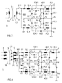
- both the DC power supply units UB1 and UB2 and the freewheeling diodes FD1 and FD2 of the two switching amplifiers as well as the filter capacitors FC1 and FC2 of the two low-pass filters are each connected in series and the connection points P2, P5 and P8 between the respective pairs of components thereof three series connections connected to each other via a continuous connecting line VL.
- the outer end points P3, P6, P9 and P4, P7, P10 of these three series connections are each connected to one another via a further series connection comprising switch SCH1 or SCH2 and filter coil FL1 or FL2, the series connection of the freewheeling diodes FD1 and FD2 with their two End points P6 and P7 are each connected between switch SCH1 and SCH2 and filter coil FL1 and FL2.
- the series connection of the two direct voltage power supply units UB1 and UB2 is realized in this amplifier module V in the form of a double power supply unit known per se and described, for example, in the TELEFUNKEN tube pocket book, edition 1956, on page 310.
- This double power supply contains a power transformer TR, which in the exemplary embodiment in FIG. 7 is, for example, single-phase with a primary winding 2 and a secondary winding 4 and which contains a shield 3 connected to ground in order to derive capacitive switching currents.
- a power transformer TR which in the exemplary embodiment in FIG. 7 is, for example, single-phase with a primary winding 2 and a secondary winding 4 and which contains a shield 3 connected to ground in order to derive capacitive switching currents.
- two rectifiers G1 and G2 Connected to one end of the secondary winding are two rectifiers G1 and G2 connected in opposite polarity in parallel ("antiparallel"), which produce two raw DC voltages with different polarity with respect to the other end P1 of the secondary winding, which consist of the respective downstream LC filter element Screen choke SL1 or SL2 and screen capacitor SC1 or SC2, screened, ie to be smoothed.
- the filter capacitors SC1 and SC2 are connected in series in this double power supply unit, their common connection point P2 being connected to the other end P1 of the secondary winding 4 via the continuous connecting line VL.
- the smoothed DC voltage applied to the respective filter capacitor SC1 or SC2 represents the output voltage of the respective DC power supply unit UB1 or UB2.
- a continuous symmetrical connection is present in the amplifier module V according to the invention between the secondary winding 4 of the mains transformer (TR) on the one hand and the filter capacitors FC1 and FC2 of the low-pass filter on the other hand, which in particular the secondary winding-related capacities of the network transformer TR directly connected to the low-pass filters and "integrated" into them.
- the great advantage of this circuit according to the invention is that with this integration, in particular the secondary winding-related capacities of the power transformer in the low-pass filter on the transformer no longer have the high sampling or switching frequencies, as in the known power amplifiers, but only the low-frequency input signal to be sampled , so that the harmful build-up capacities are only reloaded with the frequency of the input signal (and no longer with the switching frequency), with a corresponding reduction the power loss in the construction capacities of the network transformer or is associated with a corresponding improvement in the efficiency of the power amplifier.
- the known switching amplifier also uses the double power supply known per se, but in order to implement two switching amplifiers UB1, SCH1, FD1 or UB2, SCH2, FD2 connected in series, which are followed by a common low-pass filter FL, FC.
- the switches SCH1 and SCH2 of the amplifier module V according to the invention in FIGS. 7 or 8 can be controlled independently of each other, ie switched on and off.
- the pulse sequences derived from the input signal determine the chronological sequence of the switching pulses.
- the resulting output voltage U A at the output of the amplifier module V can ideally take any value between 0 volts (both switches switched off) and 2U B (both switches switched on) statically or dynamically depending on these pulse trains or the switching pulses, with U B the Output voltage of a DC power supply unit UB1 or UB2.
- the two switches SCH1 and SCH2 of the amplifier module V according to the invention are advantageously synchronized, i.e. controlled simultaneously with pulse duration modulated pulse sequences, since in this case the circuit in FIG. 8 acts like a three-phase bridge circuit, which makes it possible to make the inherently harmful construction capacities of the mains transformer harmless by integration into the low-pass filter and which at the same time has the good efficiency of a three-phase bridge circuit.
- the output capacitances CS1 and CS2 of the two switches SCH1 and SCH2 are in reality parallel to the respective freewheeling diode FD1 and FD2.
- the two freewheeling diodes FD1 and FD2 each have a series circuit made up of resistors R1 and R2 and a further switch SCH3 and SCH4 connected in parallel, which work in opposition to the two "main switches” SCH1 and SCH2 and which discharge the switching capacitances CS1 and CS2 worry.
- Dead time is provided, the duration of which is preferably approximately the discharge times of the switching capacitors CS1 and CS2 for large current values, i.e. corresponds to the top and bottom lines, so that the transfer power flows through the load resistor R for the top line and line and is only used for the underscore in the discharge resistors R1 and R2.
- either a single switch or a plurality of switches connected in series and / or in parallel must be provided to implement the switches.
- MOSFET MOS field effect transistors
- SIT static induction transistors
- SITh static induction thyristors
- GTO turn-off thyristors
- cascade or cascode circuits etc.
- the MOSFET is currently the cheapest, since it enables very short switching times (and therefore very low switching losses) to be achieved.
- the storage times typical for bipolar components are no longer required.
- the parallel connection of several MOSFETs is not a problem since, in contrast to bipolar transistors, they have a negative temperature gradient which leads to the on-state resistance of a MOSFET increasing with increasing temperature and the forward current decreases accordingly, so that the total current to be routed is automatically divided evenly between the parallel connected MOSFETs and overloading of individual MOSFETs is thereby prevented.
- a cut-off diode KD1 or KD2 is switched from amplifier output A or B to output P3 or P4 of the assigned DC voltage power supply unit UB1 or UB2 which "clamps" these overshoots in the tensions, ie cuts them off.
- the diodes KD1, KD2 need not be very fast, ie t rr can be large. You only need to be able to cut the vibrations at the resonance frequency of the low-pass filter (which in the application is a modulation amplifier for a transmitter in the kHz range).
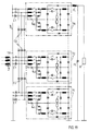
- the power amplifier in FIG. 9 consists of N similar amplifier modules V1-V N according to the invention as shown in FIG. 7 in a three-phase version, the network transformers of the individual amplifier modules V 1 -V N advantageously being a network transformer TR with a set of delta-connected primary windings 2 and with a number of amplifier modules V 1 -V N corresponding to the number of secondary winding sets 4 1 -4 N and with a grounded common shield 3 have been summarized.
- the power of the amplifier according to the invention is reduced either by forcibly switching off individual amplifier modules using the switches in the amplifier modules themselves or advantageously by means of the power protection relays (RE1-RE3 in FIG. 8) fitted between the transformer TR and rectifier circuits (G1-G6 in FIG. 8). , since in the latter case the modules concerned can also be switched off in the case of alloyed (conductive) semiconductor switches.
- the power amplifier in FIG. 10 differs from the amplifier in FIG. 9 characterized in that the individual low-pass filters in the amplifier modules V1-V N according to FIG. 8 have been carried out in two stages.
- the power amplifier in FIG. 11 differs from the amplifier in FIG. 9 in that a separate low-pass filter FL, FC is connected downstream of the power amplifier.
- FIGS. 9-11 the corresponding, in addition to shielding capacitances CT, the additional transverse capacitances CQ, already mentioned above, between spatially adjacent secondary windings 4 1 -4 N of the mains transformer TR are shown.
- the chimney capacities CT and external capacities CQ are drawn as real capacitors (with solid connecting lines) and not as capacities due to the structure (with dashed connecting lines).
- these capacities are integral components of the downstream low-pass filter in the individual amplifier modules V 1 -V N.
- these figures also do not contain any further details regarding the structure of the network transformer used (iron core, insulating materials, etc.), which, however, must nevertheless be taken into account when realizing the power amplifiers according to the invention.
- a multi-stage low-pass filter for example a two-stage low-pass filter, instead of the single-stage low-pass filter discussed above.
- a multi-stage low-pass filter for example a two-stage low-pass filter
- the advantage of the first solution (FIG. 10) can be seen above all in the full testability of the individual amplifier modules, while the second solution (FIG. 11) has the advantage that there are practically no manufacturing tolerances of the individual filter elements of the first stage can affect the quality values of the output signal of the power amplifier.
- FIG. 13 is such a supporter 6 e.g. Can be made of cast resin and inserted into the outer wall 7 of a network transformer filled with oil 8.
- the connections A1 to A8 correspond to those of FIG. 12th
- FIG. 14 shows a plan view of a support according to FIG. 13.
- the voltage data given on the outer ring are exemplary selected RMS values for DC voltage power supply units (UB1, UB2 in FIG. 8), each of which has DC voltages of approximately ⁇ 670 V with respect to the connection point P2 in FIG. Generate 7 or 8.
- pulse transmitters instead of fiber optic cables in the control and / or transmission lines of the control circuit for electrical isolation.
- the feedback signal not at the downstream low-pass filter, but at the output of the low-pass filter, which is particularly advantageous if the low-pass filter is wholly or partly integrated into the individual switching amplifiers.
Landscapes
- Engineering & Computer Science (AREA)
- Power Engineering (AREA)
- Amplifiers (AREA)
Claims (18)
- Amplificateur de puissance pour amplifier un signal d'entrée analogique (NF), comprenant N modules d'amplificateur à commutation (V), montés en série côté sortie, et un filtre passe-bas côté sortie, dans lequel les interrupteurs (SCH1; SCH2) des modules d'amplificateur (V) sont commandés par des signaux d'un circuit de commande (ST), signaux qui sont tirés du signal d'entrée (NF), dans lequel, en tant qu'amplificateurs à commutation, des amplificateurs à commutation commutés côté secondaire sont prévus dans les modules d'amplificateur (V), et dans lequel deux amplificateurs à commutation, montés directement en série l'un derrière l'autre et constitués chacun d'une alimentation tension continue (UB1; UB2), d'un interrupteur (SCH1; SCH2) et d'une diode de roue libre (FD1; FD2), sont réunis chaque fois en un module d'amplificateur (V), de manière que les alimentations tension continue (UB1; UB2) et les diodes de roue libre (FD1, FD2) des deux amplificateurs à commutation soient chaque fois connectées en série, caractérisé en ce que les amplificateurs à commutation sont commandés par des séries d'impulsions modulées en durée d'impulsion, qui sont mutuellement déphasées, qu'un montage en série composé d'un interrupteur supplémentaire (SCH3; SCH4) et d'une résistance (R1; R2) est connecté chaque fois, dans le module d'amplificateur (V), en parallèle avec la diode de roue libre (FD1; FD2) entre les deux alimentations tension continue (UB1, UB2) montées en série et les deux diodes de roue libre (FD1, FD2) connectées en série, que ces deux interrupteurs supplémentaires (SCH3, SCH4) sont commutés chaque fois de façon complémentaire, c'est-à-dire en opposition (en push-pull) avec le premier interrupteur (SCH1; SCH2) correspondant, que le filtre passe-bas (FL1, FC1; FL2, FC2) est intégré totalement ou partiellement dans les différents modules d'amplificateur (V1-VN) et que les deux condensateurs de filtrage (FC1, FC2) d'un module d'amplificateur à commutation sont connectés en série entre eux.
- Amplificateur de puissance selon la revendication 1, caractérisé en ce que le déphasage entre deux séries d'impulsions qui se succèdent directement dans le temps est chaque fois de 360°/N.
- Amplificateur de puissance selon la revendication 1 ou 2, caractérisé en ce que le circuit de commande (ST) est relié aux différents amplificateurs à commutation (V1-VN) par des lignes de commande (ST1-STN) réalisées de préférence sous la forme de câbles à fibres optiques.
- Amplificateur de puissance selon la revendication 3, caractérisé en ce que- pour générer les différentes séries d'impulsions, des modulateurs d'impulsions en durée (PDM1-PDMN), à fonctionnement numérique ou analogique, sont prévus dans le circuit de commande (ST);- chacun de ces modulateurs d'impulsions en durée (PDM1-PDMN) rest relié, côté sortie, par l'une des lignes de commande (ST1-STN), réalisées de préférence sous la forme de câbles à fibres optiques, à l'amplificateur à commutation (V1-VN) qui lui est coordonné et, côté entrée, par une première ligne de transmission (LK1-LKN), à un étage de pré-modulation (VM) qui est commun à tous les modulateurs (PDM1-PDMN); et- chacun de ces modulateurs d'impulsions en durée (PDM1-PDMN) est relié par son entrée de référence et à travers une seconde ligne de transmission (K1-KN) à un étage d'oscillateur de référence (ROS) commun à tous les modulateurs (PDM1-PDMN) et reçoit de celui-ci un signal de référence pourvu du déphasage de la série d'impulsions à générer par lui.
- Amplificateur de puissance selon la revendication 3 ou 4, caractérisé en ce qu'une partie du signal de sortie de l'amplificateur, signal qui est appliqué avant ou après le filtre passe-bas (FL, FC), est envoyée comme signal de contre-réaction (RS) au circuit de commande (ST) ou à l'étage de pré-modulation (VM) à travers un diviseur de tension (SPT).
- Amplificateur de puissance selon une des revendications 1 à 5, caractérisé en ce que- les amplificateurs à commutation (V1-VN) sont équipés de transformateurs secteur (d'alimentation à partir du secteur);- ces transformateurs secteur sont réunis en un transformateur secteur (TR) possédant un enroulement primaire (2) et un nombre d'enroulements secondaires (41-4N) correspondant au nombre des modules d'amplificateur à commutation (V1-VN);- en cas d'utilisation de transformateurs secteur comportant un blindage, les blindages sont également réunis en un blindage (3) commun relié à la masse; et- en cas de prévision d'un transformateur secteur triphasé comportant un nombre triple d'enroulements primaires, les enroulements primaires sont connectés en triangle.
- Amplificateur de puissance selon une des revendications 1 à 5, caractérisé en ce que- les amplificateurs à commutation sont équipés de transformateurs secteur (d'alimentation à partir du secteur);- ces transformateurs secteur sont réunis en deux transformateurs secteur comportant chacun un enroulement primaire et un nombre d'enroulements secondaires correspondant à la moitié du nombre des modules d'amplificateur à commutation;- les deux transformateurs secteur présentent de préférence chacun un blindage relié à la masse; et- en cas de prévision de transformateurs secteur triphasés comportant un nombre triple d'enroulements primaires, les enroulements primaires d'un transformateur sont connectés en triangle et les enroulements primaires de l'autre transformateur sont connectés en étoile.
- Amplificateur de puissance selon une des revendications 1 à 7, caractérisé en ce que- les transformateurs secteur des deux amplificateurs à commutation sont réunis en un transformateur secteur (TR) commun aux deux alimentations tension continue (UB1, UB2) et de préférence de type triphasé, avec des enroulements secondaires (4) connectés ensemble en un point neutre (P1) dans un montage en étoile;- les points de connexion (P2, P5, P8) entre les alimentations tension continue (UB1, UB2) montées en série, les diodes de roue libre (FD1, FD2) montées en série et les condensateurs de filtrage (FC1, FC2) montés en série, sont reliés directement au point neutre (P1) par une ligne de liaison (VL) traversante; et- les points terminaux (P3, P6, P9; P4, P7, P10) des trois montages en série constitués des alimentations tension continue (UB1, UB2), des diodes de roue libre (FD1, FD2) et des condensateurs de filtrage (FC1, FC2), sont chaque fois reliés entre eux par un montage en série supplémentaire formé d'un interrupteur (SCH1; SCH2) et d'une bobine de filtrage (FL1; FL2), et le montage en série des diodes de roue libre (FD1, FD2) est connecté par chacun de ses points terminaux (P6; P7) entre un interrupteur (SCH1; SCH2) et une bobine de filtrage (FL1; FL2).
- Amplificateur de puissance selon la revendication 8, caractérisé en ce que- les deux filtres passe-bas dans le module d'amplificateur (V) sont formés chacun de plusieurs étages de filtrage (FL1, FC1; FL3, FC3 ou FL2, FC2; FL4, FC4) montés l'un à la suite de l'autre;- les différents étages de filtrage contiennent chacun une bobine de filtrage (FL1-FL4) et un condensateur de filtrage (FC1-FC4) monté à la suite de la bobine de filtrage correspondante;- les bobines de filtrage (FL1, FL3 ou FL2, FL4) des différents étages de filtrage d'un filtre passe-bas sont chaque fois montées en série entre elles et les condensateurs de filtrage (FC1, FC3 ou FC2, FC4) des étages de filtrage d'un filtre passe-bas sont chaque fois montés en parallèle entre eux;- les condensateurs de filtrage (FC1, FC2 ou FC3, FC4) d'étages de filtrage de même ordre (FL1, FC1; FL2, FC2 OU FL3, FC3; FL4, FC4) des deux filtres passe-bas sont chaque fois connectés en série et- les points de connexion (P8, P8') entre deux condensateurs de filtrage (FC1, FC2 ou FC3, FC4) connectés chaque fois en série, sont reliés directement au point neutre (P1) par la ligne de liaison (VL) traversante.
- Amplificateur selon la revendication 8 ou 9, caractérisé en ce que- les deux alimentations tension continue (UB1, UB2), montées en série dans le module d'amplificateur (V), sont constituées par deux circuits redresseurs triphasés à montage en étoile (G1, G3, G5 ou G2, G4, G6) raccordés en parallèle, mais suivant des polarités contraires aux extrémités opposées au point neutre (P1) des enroulements secondaires (4) du transformateur secteur (TR), et générant, par rapport au point neutre (P1), deux tensions continues de polarités différentes, ainsi que par un élément de filtrage (SL1, SC1 ou SL2, SC2) prévu à la suite de chaque circuit redresseur et composé d'une inductance de filtrage (SL1 ou SL2) et d'un condensateur de filtrage (SC1 ou SC2); et- les condensateurs de filtrage (SC1, SC2) des deux éléments de filtrage (SL1; SC1 ou SL2, SC2) sont connectés en série et leur point de connexion commun est le point de connexion (P2) des deux alimentations tension connue (UB1, UB2), lequel est relié directement au point neutre (P1) par la ligne de liaison (VL) traversante.
- Amplificateur de puissance selon une des revendications 8 à 10, caractérisé en ce que chacun des deux points terminaux (P3; P4) du montage en série des alimentations tension continue (UB1, UB2) est relié à travers une diode d'écrêtage (KD1; KD2) à la sortie (A; B) qui lui est coordonnée du module d'amplificateur (V).
- Amplificateur de puissance selon une des revendications 8 à 11, caractérisé en ce que des relais de protection de puissance (RE1-RE3) sont montés, côté secondaire, à la suite du transformateur secteur (TR).
- Amplificateur de puissance selon une des revendications 8 à 12, caractérisé en ce que les différents modules d'amplificateur (V1-VN) sont de même structure et fournissent essentiellement des signaux de sortie identiques.
- Amplificateur de puissance selon une des revendications 8 à 13, caractérisé en ce que les interrupteurs (SCH1-SCH4) dans les différents modules d'amplificateur (V) sont formés chaque fois d'un interrupteur à semi-conducteur ou de plusieurs interrupteurs à semi-conducteurs montés en série et/ou en parallèle.
- Amplificateur de puissance selon la revendication 14, caractérisé en ce que les interrupteurs à semi-conducteurs sont des transistors à effet de champ MOS (MOSFET), des transistors à induction statique (SIT), des thyristors à induction statique (SITh) ou des thyristors de blocage (GTO), des montages en cascade ou des montages en cascode.
- Amplificateur de puissance selon une des revendications 8 à 15, caractérisé en ce que les modules d'amplificateur (V₁-VN), montés en série par leurs sorties, sont suivis d'un filtre passe-bas supplémentaire (FL, FC).
- Amplificateur de puissance selon une des revendications 1 à 16, caractérisé par son application comme amplificateur de modulation pour des émetteurs, en particulier comme amplificateur de modulation pour des émetteurs radioélectriques haute puissance modulés en amplitude de la gamme des grandes, moyennes et courtes ondes, avec un tube d'étage final RF à modulation d'anode.
- Amplificateur de puissance selon une des revendications 1 à 16, caractérisé par son application comme alimentation courant continu à haute tension, en particulier pour l'alimentation d'électroaimants dans les installations d'accélérateurs de particules.
Applications Claiming Priority (2)
| Application Number | Priority Date | Filing Date | Title |
|---|---|---|---|
| DE3822990 | 1988-07-07 | ||
| DE3822990A DE3822990A1 (de) | 1988-07-07 | 1988-07-07 | Leistungsverstaerker |
Publications (2)
| Publication Number | Publication Date |
|---|---|
| EP0349732A1 EP0349732A1 (fr) | 1990-01-10 |
| EP0349732B1 true EP0349732B1 (fr) | 1994-04-27 |
Family
ID=6358145
Family Applications (1)
| Application Number | Title | Priority Date | Filing Date |
|---|---|---|---|
| EP89108457A Expired - Lifetime EP0349732B1 (fr) | 1988-07-07 | 1989-05-11 | Amplificateur de puissance |
Country Status (2)
| Country | Link |
|---|---|
| EP (1) | EP0349732B1 (fr) |
| DE (2) | DE3822990A1 (fr) |
Families Citing this family (13)
| Publication number | Priority date | Publication date | Assignee | Title |
|---|---|---|---|---|
| DE3907919A1 (de) * | 1988-07-07 | 1990-01-11 | Olympia Aeg | Leistungsverstaerker |
| US5200707A (en) * | 1990-06-05 | 1993-04-06 | Continental Electronics Corporation | Amplifier with multiple switched stages and noise suppression |
| WO1995010881A1 (fr) * | 1993-10-11 | 1995-04-20 | Thomcast Ag | Amplificateur a decoupage |
| JP2885660B2 (ja) * | 1995-01-31 | 1999-04-26 | 日本無線株式会社 | 振幅変調回路 |
| DE19812069B4 (de) * | 1998-03-19 | 2005-07-07 | Siemens Ag | Leistungsverstärker und Verfahren zum Erzeugen von Steuersignalen für einen Leistungsverstärker |
| DE19824768B4 (de) * | 1998-06-03 | 2005-06-09 | Siemens Ag | Leistungsverstärker und Verfahren zum Ansteuern eines Leistungsverstärkers |
| DE19857525C2 (de) | 1998-12-14 | 2003-03-06 | Siemens Ag | Leistungsverstärker |
| US6172558B1 (en) | 1999-09-02 | 2001-01-09 | Siemens Aktiengesellschaft | Switching amplifier and method for operating same |
| DE10048593B4 (de) * | 2000-09-30 | 2009-07-16 | Infineon Technologies Ag | Schaltungsanordnung mit einem Pulsweitenmodulator zur Ansteuerung einer Last |
| DE10048962B4 (de) * | 2000-10-04 | 2006-12-07 | Omicron Electronics Gmbh | Tragbare Prüfeinrichtung zum Prüfen von mit hohen Spannungen und/oder hohen Strömen zu betreibenden Prüflingen und Prüfsystem |
| JP3499235B1 (ja) * | 2002-08-28 | 2004-02-23 | 株式会社フライングモール | スイッチング回路及びディジタル電力増幅器 |
| CN109555167A (zh) * | 2017-09-27 | 2019-04-02 | 中国二十冶集团有限公司 | 一种用于碎石桩密实度检测的断面分析方法 |
| CN117055094A (zh) * | 2023-07-27 | 2023-11-14 | 电子科技大学 | 一种用于震电测井的脉冲声源 |
Family Cites Families (10)
| Publication number | Priority date | Publication date | Assignee | Title |
|---|---|---|---|---|
| US4164714A (en) * | 1977-09-26 | 1979-08-14 | Harris Corporation | Polyphase PDM amplifier |
| DE2935445A1 (de) * | 1979-08-09 | 1981-02-26 | Bbc Brown Boveri & Cie | Nf-leistungsverstaerker |
| GB2064901B (en) * | 1979-11-30 | 1984-11-07 | Harris Corp | Digital high power amplifier |
| EP0058443B1 (fr) * | 1981-02-16 | 1985-07-10 | BBC Brown Boveri AG | Procédé pour amplifier un signal analogique à basse fréquence au moyen d'un amplificateur à commutation et amplificateur à commutation pour la mise en oeuvre du dit procédé |
| DE3265563D1 (en) * | 1981-06-01 | 1985-09-26 | Bbc Brown Boveri & Cie | Switching amplifier |
| DE3447566A1 (de) * | 1984-12-21 | 1986-07-03 | Licentia Patent-Verwaltungs-Gmbh, 6000 Frankfurt | Pulsstufenmodulierter schaltverstaerker |
| DE3502135A1 (de) * | 1985-01-19 | 1986-07-24 | Licentia Patent-Verwaltungs-Gmbh, 6000 Frankfurt | Schaltungsanordnung eines schaltverstaerkers |
| DE3632716A1 (de) * | 1986-09-26 | 1988-03-31 | Licentia Gmbh | Schneller digitaler leistungsverstaerker |
| DE3635365A1 (de) * | 1986-10-17 | 1988-04-21 | Licentia Gmbh | Sekundaerseitig schaltbares netzgeraet |
| DE3637934A1 (de) * | 1986-11-07 | 1988-05-19 | Licentia Gmbh | Schaltverstaerker |
-
1988
- 1988-07-07 DE DE3822990A patent/DE3822990A1/de not_active Ceased
-
1989
- 1989-05-11 DE DE58907550T patent/DE58907550D1/de not_active Expired - Fee Related
- 1989-05-11 EP EP89108457A patent/EP0349732B1/fr not_active Expired - Lifetime
Also Published As
| Publication number | Publication date |
|---|---|
| DE3822990A1 (de) | 1990-01-11 |
| DE58907550D1 (de) | 1994-06-01 |
| EP0349732A1 (fr) | 1990-01-10 |
Similar Documents
| Publication | Publication Date | Title |
|---|---|---|
| EP0349732B1 (fr) | Amplificateur de puissance | |
| DE69212355T2 (de) | Vorrichtung für die galvanische Trennung von Gleichstromsignalen oder eine Gleichstromkomponente enthaltendes Signal | |
| EP0231481A2 (fr) | Convertisseur courant alternatif - courant continu avec circuit en demi-pont asymétrique | |
| DE2108608A1 (de) | Wechselrichter | |
| DE10392579T5 (de) | Aktiver Common Mode Emi Filter | |
| WO2021063593A1 (fr) | Convertisseur de puissance bidirectionnel ayant un circuit intermédiaire | |
| EP0682402B1 (fr) | Dispositif pour la limitation de la pente des grandeurs de sortie d'un convertisseur auto-commuté à circuit intermédiaire à tension continue | |
| EP0349743A2 (fr) | Amplificateur de puissance | |
| DE69802264T2 (de) | Rekonstruktionsfilter zur unterdrückung von schaltrestströmen in einem geschalteten system oder ähnlichem | |
| DE69011550T2 (de) | Tonfrequenzverstärker mit phasenmodulierter Pulsbreitenmodulation. | |
| CH713573B1 (de) | Magnetische Drossel, Umrichterabschnitt und Umrichter. | |
| EP0108194A1 (fr) | Circuit amplificateur sélectif du type push-pull | |
| EP0267391B1 (fr) | Amplificateur à commutation | |
| EP0211210B1 (fr) | Amplificateur à commutation | |
| DE60112735T2 (de) | Geschalteter hochfrequenzleistungsverstärker | |
| DE69725788T2 (de) | Nullspannungsschaltender VHF Serienresonanzwechselrichter mit mehreren Ausgängen | |
| EP0263936B1 (fr) | Alimentation de puissance à commutation sur le circuit secondaire | |
| DE69909086T2 (de) | Schaltung und deren Verwendung zur Reduzierung von Verzerrungen und Störungen von Rechteckimpulsen | |
| DE3833700C2 (fr) | ||
| DE3316281C2 (de) | Schaltnetzteil zur Gleichspannungswandlung | |
| CH649877A5 (de) | Vorrichtung mit einem niederfrequenzverstaerker. | |
| DE3545770C2 (fr) | ||
| EP2262087A1 (fr) | Circuit convertisseur | |
| DE3502135A1 (de) | Schaltungsanordnung eines schaltverstaerkers | |
| DE10226889B4 (de) | Frequenzverdoppler |
Legal Events
| Date | Code | Title | Description |
|---|---|---|---|
| PUAI | Public reference made under article 153(3) epc to a published international application that has entered the european phase |
Free format text: ORIGINAL CODE: 0009012 |
|
| AK | Designated contracting states |
Kind code of ref document: A1 Designated state(s): CH DE FR GB LI |
|
| 17P | Request for examination filed |
Effective date: 19900207 |
|
| 17Q | First examination report despatched |
Effective date: 19920806 |
|
| RAP1 | Party data changed (applicant data changed or rights of an application transferred) |
Owner name: TELEFUNKEN SENDERTECHNIK GMBH |
|
| GRAA | (expected) grant |
Free format text: ORIGINAL CODE: 0009210 |
|
| AK | Designated contracting states |
Kind code of ref document: B1 Designated state(s): CH DE FR GB LI |
|
| REF | Corresponds to: |
Ref document number: 58907550 Country of ref document: DE Date of ref document: 19940601 |
|
| ET | Fr: translation filed | ||
| GBT | Gb: translation of ep patent filed (gb section 77(6)(a)/1977) |
Effective date: 19940729 |
|
| PLBE | No opposition filed within time limit |
Free format text: ORIGINAL CODE: 0009261 |
|
| STAA | Information on the status of an ep patent application or granted ep patent |
Free format text: STATUS: NO OPPOSITION FILED WITHIN TIME LIMIT |
|
| 26N | No opposition filed | ||
| PGFP | Annual fee paid to national office [announced via postgrant information from national office to epo] |
Ref country code: DE Payment date: 19990504 Year of fee payment: 11 |
|
| PGFP | Annual fee paid to national office [announced via postgrant information from national office to epo] |
Ref country code: FR Payment date: 19990505 Year of fee payment: 11 |
|
| PGFP | Annual fee paid to national office [announced via postgrant information from national office to epo] |
Ref country code: GB Payment date: 19990507 Year of fee payment: 11 |
|
| PGFP | Annual fee paid to national office [announced via postgrant information from national office to epo] |
Ref country code: CH Payment date: 19990819 Year of fee payment: 11 |
|
| PG25 | Lapsed in a contracting state [announced via postgrant information from national office to epo] |
Ref country code: GB Free format text: LAPSE BECAUSE OF NON-PAYMENT OF DUE FEES Effective date: 20000511 |
|
| PG25 | Lapsed in a contracting state [announced via postgrant information from national office to epo] |
Ref country code: LI Free format text: LAPSE BECAUSE OF NON-PAYMENT OF DUE FEES Effective date: 20000531 Ref country code: CH Free format text: LAPSE BECAUSE OF NON-PAYMENT OF DUE FEES Effective date: 20000531 |
|
| GBPC | Gb: european patent ceased through non-payment of renewal fee |
Effective date: 20000511 |
|
| REG | Reference to a national code |
Ref country code: CH Ref legal event code: PL |
|
| PG25 | Lapsed in a contracting state [announced via postgrant information from national office to epo] |
Ref country code: FR Free format text: LAPSE BECAUSE OF NON-PAYMENT OF DUE FEES Effective date: 20010131 |
|
| PG25 | Lapsed in a contracting state [announced via postgrant information from national office to epo] |
Ref country code: DE Free format text: LAPSE BECAUSE OF NON-PAYMENT OF DUE FEES Effective date: 20010301 |
|
| REG | Reference to a national code |
Ref country code: FR Ref legal event code: ST |