EP0349757A2 - Dispositif et méthode de traduction d'adresse virtuelle en adresse réelle améliorée pour accéder à une mémoire cache - Google Patents
Dispositif et méthode de traduction d'adresse virtuelle en adresse réelle améliorée pour accéder à une mémoire cache Download PDFInfo
- Publication number
- EP0349757A2 EP0349757A2 EP89109786A EP89109786A EP0349757A2 EP 0349757 A2 EP0349757 A2 EP 0349757A2 EP 89109786 A EP89109786 A EP 89109786A EP 89109786 A EP89109786 A EP 89109786A EP 0349757 A2 EP0349757 A2 EP 0349757A2
- Authority
- EP
- European Patent Office
- Prior art keywords
- address
- comparison
- cache
- unit
- signal group
- Prior art date
- Legal status (The legal status is an assumption and is not a legal conclusion. Google has not performed a legal analysis and makes no representation as to the accuracy of the status listed.)
- Granted
Links
Images

Classifications
-
- G—PHYSICS
- G06—COMPUTING OR CALCULATING; COUNTING
- G06F—ELECTRIC DIGITAL DATA PROCESSING
- G06F12/00—Accessing, addressing or allocating within memory systems or architectures
- G06F12/02—Addressing or allocation; Relocation
- G06F12/08—Addressing or allocation; Relocation in hierarchically structured memory systems, e.g. virtual memory systems
- G06F12/10—Address translation
- G06F12/1027—Address translation using associative or pseudo-associative address translation means, e.g. translation look-aside buffer [TLB]
- G06F12/1045—Address translation using associative or pseudo-associative address translation means, e.g. translation look-aside buffer [TLB] associated with a data cache
- G06F12/1054—Address translation using associative or pseudo-associative address translation means, e.g. translation look-aside buffer [TLB] associated with a data cache the data cache being concurrently physically addressed
Definitions
- This invention relates generally to the cache memory units associated with central processing units of data processing systems and, more particularly, to the accessing of the cache memory unit by the central processing unit.
- each signal group has an address associated therewith.
- the address is used for identifying a location in the data processing system main memory unit and can act as an identifier of the signal group itself.
- a signal group can have at least two addresses (i.e., identifiers), a virtual address, the address by which the central processing unit identifies the signal group, and a real address, the address which identifies a particular location in the data processing system main memory unit.
- the modern data processing system typically includes a cache memory unit associated with the central processing unit.
- the cache memory unit acts as a buffer mechanism between the relatively slow retrieval of signal groups from the main memory unit and the immediacy requirement of the central processing unit for requested signal groups.
- the cache memory unit stores signal groups that have a high probability of requirement by the central processing unit.
- the location in which a signal group is stored in a cache memory unit is related to the real address as will be clear to those familiar with the related art.
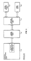
- the main memory unit 13 stores the data signal groups required by the central prccessing unit 14 to execute the desired procedures.
- Signal groups with a high probability for requirement by the central processing unit 11 from the main memory unit 13 or a user unit 15 are transferred through a system interface unit 11 to the cache memory unit 12.
- the signal groups are transferred over a system bus, thereby requiring an interface unit for each component interacting with the system bus.
- the signal groups are stored in the cache memory unit 12 until requested by central processing unit 14.
- address translation apparatus 141 converts the virtual address, used by the central processing unit 14 to identify the signal group, to the real address used for that signal group by the remainder of the data processing system to identify the signal group.
- the address translation apparatus is typically initialized and maintained by the data processing system operating system. After processing in the central processing unit 14, the signal group is returned tc the cache memory unit 12 at an address determined by the address translation apparatus and consequently transferred to the user unit 15 or main memory unit 13, as specified by the program.
- a virtual address 21 of a signal group to be accessed is provided by the central processing unit, typically in a register 23.
- the virtual address includes at least two portions, a WORD portion 21A consisting of n logic bit positions and a VIRTUAL PAGE NUMBER portion 21B consisting of m logic bit positions.
- the WORD portion 21A of the virtual address 21 is used, unchanged, as the WORD portion 23A, while the VIRTUAL PAGE NUMBER portion 21B of the virtual address is applied to an associative memory 22.
- the signal group accessed in the associative memory 22 as a result of the application of the VIRTUAL PAGE NUMBER portion 21B thereto becomes the m logic bits of the REAL PAGE NUMBER portion 23B stored in register 23.
- This address translation is typically implemented to be completed in one clock cycle T0.
- the real address stored in register 23 is now used to access the contents of the cache memory unit 25.
- To the n bit positions of the WORD portion 23A of the real address are added b bits from the REAL PAGE NUMBER portion 23B to form a LOCATION address and the LOCATION address is applied to address in terminals of cache directory unit 251 and the address in terminals of cache storage unit 252.
- identified by the LOCATION address, in the cache storage unit can be, under appropriate conditions, the signal group which is the signal group required by the central processing unit.
- identified by the LOCATION address, in the cache directory unit is stored the signal group corresponding to the logic signals stored in the m-b bit positions of the REAL PAGE NUMBER portion 23B, generally referred to as the COMPARISON address, of the real address of the signal group stored in the addressed location of the cache storage unit.
- the location address and the (COMPARISON) address signal group stored in the cache directory unit together form the address of the signal group stored at the corresponding location in the cache storage unit.
- the plurality of signal groups, generally referred to as levels, stored at the addressed location are applied to multiplexer unit 254.
- a signal group stored therein is compared with the remaining m-b signals of the REAL PAGE NUMBER portion 23B of the real address 23 in comparison unit 253.
- the signal group at the LOCATION address is identified by the real address 23 and a selected signal group (or level identified by signals from the comparison unit) is transferred by multiplexer unit 254 to the central processing unit.
- this signal is transmitted to the central processing unit for appropriate response, typically retrieval of the identified signal group from the main memory unit.
- the cache memory unit access requires a second system clock cycle T0.
- the plurality of signal groups (or levels) stored at each location in the cache storage unit is used to reduce the time needed to retrieve a signal group from the cache memory unit.
- a desirable improvement would be the storage of a single signal group at each memory location.
- U.S. Patent 3,979,726; U.S. Patent 4,264,953 and U.S. Patent 4,669,043 discuss the use of virtual addresses in combination with cache memory units, but do not describe techniques for speeding the translation of virtual addresses to real addresses.
- U.S. Patent 4,332,010 describes a cache memory unit in which the location address is the WORD (non-translatable) portion, thereby limiting the size of the cache memory unit.
- U.S. Patent 3,723,976; U.S. Patent 4,612,612 and U.S. patent 4,682,281 contain apparatus responsive to virtual addresses and apparatus responsive to real addresses fcr accessing cache memory signal groups, thereby greatly expanding the apparatus and the complexity of the data processing system.
- a small associative memory responsive to at least a portion of the virtual address, that stores trial bits of the cache memory unit location address to be used until the translation of the virtual page number to the real page number can provide the correct bits of the cache memory location address.
- the stored bits are used, in conjunction with the location address logic bits that do not require translation, to access a location in the cache directory unit prior to the development of the real address required in such an access.
- the translation from the virtual address is complete.
- the translated portion of the real address that is to be used in the comparison with the signal group from the cache directory unit is available and the comparison can be performed when the stored bits used in the cache memory unit location address are the same as the translated bits.
- the trial and the translated bits of the location address are the same and the comparison of the real address translated logic signals is the same as the corresponding address logic signals stored in the cache directory unit, then the contents of the cache storage unit are the desired signal group.
- the stored and translated location address logic signals are not identical, then the real address, available from translation procedure, is applied to the cache memory unit in mode of operation similar to the typical cache memory unit operation.
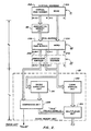
- Fig. 3 is a redrawing of Fig. 2 with the additional apparatus of the present invention and with the components of the cache memory unit arranged to emphasize the signal flow.
- the central processing unit provides a VIRTUAL PAGE NUMBER PORTION 21B address in register 21 to the address translation apparatus represented by associative memory unit 22. Simultaneously, the VIRTUAL PAGE NUMBER 21B or a portion thereof is applied to small associative memory unit 31.
- the small associative memory 31 responsive to at least a portion of the virtual address, has a relatively small number of directly accessed storage locations provident relatively small signal groups, thereby permitting identification of an associated signal group without significant delay.
- the signal group developed by the small associative memory unit 31 contains a trial signal group to complete, along with the WORD portion 21A, a TRIAL LOCATION ADDRESS.
- the TRIAL LOCATION ADDRESS is applied to address in terminals of the cache directory unit 251.
- the contents of the cache directory unit 251 determined by the TRIAL LOCATION ADDRESS are stored in comparison unit 253.
- the application of the VIRTUAL PAGE NUMBER 21B to the associative memory unit 22 results in the storage of the REAL PAGE NUMBER 23B in appropriate locations of register 23.
- the portion of the REAL PAGE NUMBER 23B that forms part of the LOCATION ADDRESS 24A is applied to comparison unit 32 and compared with the signal group from the small associative memory unit 31.
- a positive comparison from comparison unit indicates that the correct location in the cache directory unit 251 has been addressed by the TRIAL LOCATION ADDRESS.
- the portion of the REAL PAGE NUMBER 23B that is the COMPARISON ADDRESS is applied to the comparison unit 253 and compared with the contents from the cache directory unit, the comparison unit 253 being enabled by TRUE signal (or positive comparison from the comparison unit 32).
- TRUE signal or positive comparison from the comparison unit 32.
- a FALSE signal is generated and applied to the central processing unit.
- the FALSE signal from comparison unit 253 indicates that the signal group required by the data processing unit is not stored in the cache storage unit 252 and the required signal group must be retrieved from the main memory unit.
- multiplexer unit 36 which has the LOCATION ADDRESS applied thereto has the LOCATION ADDRESS applied to the address in terminals of the cache storage unit 252.
- the result of the application of the LOCATION ADDRESS is to apply the required signal group to the output register 354.
- the cache storage locations contain only one signal group and, therefore, an output multiplexer is not required.
- the comparison unit 32 When the comparison unit 32 provides a FALSE signal, indicating that the TRIAL LOCATION ADDRESS is not the correct LOCATION ADDRESS, as a result of the comparison operation, the FALSE signal is applied to multiplexer unit 36. By the time of the generation of the FALSE signal from comparison unit 32, the correct LOCATION ADDRESS 24A is available in register 23. As a result of the application of the FALSE signal to multiplexer unit 36, the LOCATION ADDRESS 24A is applied to address in terminals of the cache directory unit 2551. The location addressed as a consequence of the application of the LOCATION ADDRESS are entered in comparison unit 253 and compared with the COMPARISON ADDRESS 24B.
- a FALSE signal will indicate to the central processing unit that the required data signal group is not stored in the cache memory unit 25 while a TRUE signal causes the LOCATION ADDRESS to be applied (from multiplexer unit 36) to the address in terminals of cache storage unit 252 and the required signal group to be applied to output register 254.
- a second FALSE signal is shown originating from the comparison unit 32.
- the signal is used to freeze the contents of the data signal group in register 21 and register 23 in order that a second access of the cache directory unit can be accomplished without interference from the next virtual address signal group.
- the small associative memory 32 is updated by storing the portion of the REAL PAGE NUMBER 23B that is included in the LOCATION ADDRESS at a location determined by the VIRTUAL PAGE NUMBER.
- the operation of the cache directory and the operation of the virtual to real address translation, which operations are performed in parallel, can be implemented in one system clock cycle T0, while the withdrawal of the required signal group can be performed in the next consecutive cycle T0.
- the effectiveness of the present invention relies on the fact that a software program will typically reference signal groups in only a few memory data pages for extended portions of the program. As a result, only a limited number REAL PAGE NUMBER 23A signal groups will be required. Therefore, a small associative cache memory unit (31) can accommodate REAL PAGE NUMBER portions of the memory data pages currently being accessed by the central processing unit. (It will be clear that the entire VIRTUAL PAGE NUMBER 21B need not be applied to small associative memory unit 31 and that a portion thereof can be sufficient). Thus, the small associative memory unit permits an assumption to be made concerning the results of the virtual to real address translation.
- the contents of the small associative storage unit 31 can be determined, in the preferred embodiment, by entering the b signal bits from the REAL PAGE NUMBER into the location addressed by the VIRTUAL PAGE NUMBER. To the extent that the central processing unit continues to reference the same or relatively few virtual page numbers for extended periods of a procedure, the small associative memory will provide an accurate TRIAL ADDRESS, thereby enhancing performance.
- the invention uses two system clock cycles, i.e., 2 ⁇ T0, similar to the prior art implementation illustrated in Fig. 2.
- the cache memory unit 25 is pipelined such that a wrong assumption concerning the LOCATION ADDRESS portion derived from the VIRTUAL PAGE NUMBER (i.e., via the small associative memory unit 31) results in the cache memory unit retrieval cycle while a series of correct assumptions permits a signal group to be retrieved from the cache memory unit every system clock cycle T0.
- the disclosed apparatus has the further advantage that the implementing apparatus is relatively simple and can be conveniently included with cache memory unit.
- the appropriate level signal group of the plurality of levels of signal groups typically associated with each cache storage level address can be selected so that only the required signal group need be transferred to the central processing unit.
Landscapes
- Engineering & Computer Science (AREA)
- Theoretical Computer Science (AREA)
- Physics & Mathematics (AREA)
- General Engineering & Computer Science (AREA)
- General Physics & Mathematics (AREA)
- Memory System Of A Hierarchy Structure (AREA)
- Techniques For Improving Reliability Of Storages (AREA)
Applications Claiming Priority (2)
| Application Number | Priority Date | Filing Date | Title |
|---|---|---|---|
| US20349088A | 1988-06-07 | 1988-06-07 | |
| US203490 | 1989-06-07 |
Publications (3)
| Publication Number | Publication Date |
|---|---|
| EP0349757A2 true EP0349757A2 (fr) | 1990-01-10 |
| EP0349757A3 EP0349757A3 (en) | 1990-09-19 |
| EP0349757B1 EP0349757B1 (fr) | 1996-07-17 |
Family
ID=22754220
Family Applications (1)
| Application Number | Title | Priority Date | Filing Date |
|---|---|---|---|
| EP89109786A Expired - Lifetime EP0349757B1 (fr) | 1988-06-07 | 1989-05-31 | Dispositif et méthode de traduction d'adresse virtuelle en adresse réelle améliorée pour accéder à une mémoire cache |
Country Status (13)
| Country | Link |
|---|---|
| EP (1) | EP0349757B1 (fr) |
| JP (1) | JPH0251755A (fr) |
| KR (1) | KR930002314B1 (fr) |
| CN (1) | CN1024600C (fr) |
| AU (1) | AU612035B2 (fr) |
| CA (1) | CA1328026C (fr) |
| DE (1) | DE68926837T2 (fr) |
| ES (1) | ES2090023T3 (fr) |
| FI (1) | FI96645C (fr) |
| HR (1) | HRP921095A2 (fr) |
| MX (1) | MX173010B (fr) |
| NO (1) | NO176633C (fr) |
| YU (1) | YU117089A (fr) |
Families Citing this family (2)
| Publication number | Priority date | Publication date | Assignee | Title |
|---|---|---|---|---|
| US6965922B1 (en) * | 2000-04-18 | 2005-11-15 | International Business Machines Corporation | Computer system and method with internal use of networking switching |
| US7146484B2 (en) | 2004-06-15 | 2006-12-05 | Hitachi, Ltd. | Method and apparatus for caching storage system |
Family Cites Families (9)
| Publication number | Priority date | Publication date | Assignee | Title |
|---|---|---|---|---|
| JPS51140521A (en) * | 1975-05-30 | 1976-12-03 | Nec Corp | Address exchange device |
| JPS51145227A (en) * | 1975-06-09 | 1976-12-14 | Nec Corp | Buffer memory system |
| US4170039A (en) * | 1978-07-17 | 1979-10-02 | International Business Machines Corporation | Virtual address translation speed up technique |
| JPS5696334A (en) * | 1979-12-28 | 1981-08-04 | Fujitsu Ltd | Prefetch system |
| US4332010A (en) * | 1980-03-17 | 1982-05-25 | International Business Machines Corporation | Cache synonym detection and handling mechanism |
| JPS6049944B2 (ja) * | 1980-12-29 | 1985-11-06 | 富士通株式会社 | バッファ記憶制御方式 |
| US4400774A (en) * | 1981-02-02 | 1983-08-23 | Bell Telephone Laboratories, Incorporated | Cache addressing arrangement in a computer system |
| JPS5975482A (ja) * | 1982-10-22 | 1984-04-28 | Fujitsu Ltd | バツフア・ストレ−ジ制御方式 |
| EP0206050A3 (fr) * | 1985-06-28 | 1990-03-14 | Hewlett-Packard Company | Antémémoire à étiquettes physiques adressée virtuellement |
-
1989
- 1989-05-31 EP EP89109786A patent/EP0349757B1/fr not_active Expired - Lifetime
- 1989-05-31 DE DE68926837T patent/DE68926837T2/de not_active Expired - Fee Related
- 1989-05-31 ES ES89109786T patent/ES2090023T3/es not_active Expired - Lifetime
- 1989-06-01 AU AU35924/89A patent/AU612035B2/en not_active Ceased
- 1989-06-06 NO NO892310A patent/NO176633C/no unknown
- 1989-06-06 CA CA000601865A patent/CA1328026C/fr not_active Expired - Fee Related
- 1989-06-06 MX MX016332A patent/MX173010B/es unknown
- 1989-06-06 CN CN89103944A patent/CN1024600C/zh not_active Expired - Fee Related
- 1989-06-07 YU YU117089A patent/YU117089A/sh unknown
- 1989-06-07 JP JP89145015A patent/JPH0251755A/ja active Pending
- 1989-06-07 FI FI892779A patent/FI96645C/fi not_active IP Right Cessation
- 1989-06-07 KR KR1019890007893A patent/KR930002314B1/ko not_active Expired - Fee Related
-
1992
- 1992-10-23 HR HRP921095AA patent/HRP921095A2/hr not_active Application Discontinuation
Also Published As
| Publication number | Publication date |
|---|---|
| DE68926837T2 (de) | 1997-03-06 |
| NO892310L (no) | 1989-12-08 |
| JPH0251755A (ja) | 1990-02-21 |
| CN1040446A (zh) | 1990-03-14 |
| EP0349757B1 (fr) | 1996-07-17 |
| CN1024600C (zh) | 1994-05-18 |
| AU3592489A (en) | 1989-12-14 |
| FI96645B (fi) | 1996-04-15 |
| CA1328026C (fr) | 1994-03-22 |
| NO892310D0 (no) | 1989-06-06 |
| AU612035B2 (en) | 1991-06-27 |
| FI892779A7 (fi) | 1989-12-08 |
| MX173010B (es) | 1994-01-28 |
| FI96645C (fi) | 1996-07-25 |
| HRP921095A2 (hr) | 1994-04-30 |
| KR900000773A (ko) | 1990-01-31 |
| YU117089A (sh) | 1992-07-20 |
| DE68926837D1 (de) | 1996-08-22 |
| ES2090023T3 (es) | 1996-10-16 |
| EP0349757A3 (en) | 1990-09-19 |
| KR930002314B1 (ko) | 1993-03-29 |
| NO176633C (no) | 1995-05-03 |
| NO176633B (no) | 1995-01-23 |
| FI892779A0 (fi) | 1989-06-07 |
Similar Documents
| Publication | Publication Date | Title |
|---|---|---|
| US4811215A (en) | Instruction execution accelerator for a pipelined digital machine with virtual memory | |
| US4322815A (en) | Hierarchical data storage system | |
| US4733350A (en) | Improved purge arrangement for an address translation control system | |
| US4495575A (en) | Information processing apparatus for virtual storage control system | |
| EP0507066A1 (fr) | Verrouillage mutuel de propriété pour unités de données de cache | |
| US4755936A (en) | Apparatus and method for providing a cache memory unit with a write operation utilizing two system clock cycles | |
| JPS6255736A (ja) | デジタルプロセッサ制御装置 | |
| US5924126A (en) | Method and apparatus for providing address translations for input/output operations in a computer system | |
| CA2058259C (fr) | Appareil permettant d'augmenter le nombre de coincidences dans le repertoire des pages actives | |
| US5341484A (en) | Virtual machine system having an extended storage | |
| US5226132A (en) | Multiple virtual addressing using/comparing translation pairs of addresses comprising a space address and an origin address (sto) while using space registers as storage devices for a data processing system | |
| US5479629A (en) | Method and apparatus for translation request buffer and requestor table for minimizing the number of accesses to the same address | |
| EP0730228A1 (fr) | Organisation de mémoire protégée par ECC avec accès lecture-modification-écriture en pipeline | |
| US4648033A (en) | Look-aside buffer LRU marker controller | |
| US5652860A (en) | Memory control device | |
| EP0349757A2 (fr) | Dispositif et méthode de traduction d'adresse virtuelle en adresse réelle améliorée pour accéder à une mémoire cache | |
| US4598361A (en) | Allocator for a reduction processor evaluating programs stored as binary directed graphs employing variable-free applicative language codes | |
| JPS59112479A (ja) | キヤツシユメモリの高速アクセス方式 | |
| GB2037466A (en) | Computer with cache memory | |
| EP0362366B1 (fr) | Commande "flush-on-rei" d'antememoire d'instruction | |
| JPH0679296B2 (ja) | 多重仮想アドレス空間アクセス方法およびデータ処理装置 | |
| JPS6134628A (ja) | タグ付計算機 | |
| JP2000172675A (ja) | リストベクトル処理装置 | |
| JPS62171058A (ja) | アドレス変換装置 | |
| JPH02204848A (ja) | アドレス翻訳を採用したコンピュータ装置 |
Legal Events
| Date | Code | Title | Description |
|---|---|---|---|
| PUAI | Public reference made under article 153(3) epc to a published international application that has entered the european phase |
Free format text: ORIGINAL CODE: 0009012 |
|
| AK | Designated contracting states |
Kind code of ref document: A2 Designated state(s): DE ES FR GB IT |
|
| PUAL | Search report despatched |
Free format text: ORIGINAL CODE: 0009013 |
|
| AK | Designated contracting states |
Kind code of ref document: A3 Designated state(s): DE ES FR GB IT |
|
| 17P | Request for examination filed |
Effective date: 19901217 |
|
| 17Q | First examination report despatched |
Effective date: 19940211 |
|
| RAP1 | Party data changed (applicant data changed or rights of an application transferred) |
Owner name: BULL HN INFORMATION SYSTEMS INC. |
|
| RAP1 | Party data changed (applicant data changed or rights of an application transferred) |
Owner name: BULL HN INFORMATION SYSTEMS INC. |
|
| GRAH | Despatch of communication of intention to grant a patent |
Free format text: ORIGINAL CODE: EPIDOS IGRA |
|
| ITF | It: translation for a ep patent filed | ||
| GRAA | (expected) grant |
Free format text: ORIGINAL CODE: 0009210 |
|
| AK | Designated contracting states |
Kind code of ref document: B1 Designated state(s): DE ES FR GB IT |
|
| REF | Corresponds to: |
Ref document number: 68926837 Country of ref document: DE Date of ref document: 19960822 |
|
| REG | Reference to a national code |
Ref country code: ES Ref legal event code: FG2A Ref document number: 2090023 Country of ref document: ES Kind code of ref document: T3 |
|
| ET | Fr: translation filed | ||
| ET | Fr: translation filed | ||
| REG | Reference to a national code |
Ref country code: ES Ref legal event code: FG2A Ref document number: 2090023 Country of ref document: ES Kind code of ref document: T3 |
|
| PLBE | No opposition filed within time limit |
Free format text: ORIGINAL CODE: 0009261 |
|
| STAA | Information on the status of an ep patent application or granted ep patent |
Free format text: STATUS: NO OPPOSITION FILED WITHIN TIME LIMIT |
|
| 26N | No opposition filed | ||
| PGFP | Annual fee paid to national office [announced via postgrant information from national office to epo] |
Ref country code: ES Payment date: 19990519 Year of fee payment: 11 |
|
| PG25 | Lapsed in a contracting state [announced via postgrant information from national office to epo] |
Ref country code: ES Free format text: THE PATENT HAS BEEN ANNULLED BY A DECISION OF A NATIONAL AUTHORITY Effective date: 20000601 |
|
| REG | Reference to a national code |
Ref country code: GB Ref legal event code: IF02 |
|
| REG | Reference to a national code |
Ref country code: ES Ref legal event code: FD2A Effective date: 20020204 |
|
| PGFP | Annual fee paid to national office [announced via postgrant information from national office to epo] |
Ref country code: DE Payment date: 20050502 Year of fee payment: 17 |
|
| PGFP | Annual fee paid to national office [announced via postgrant information from national office to epo] |
Ref country code: FR Payment date: 20050530 Year of fee payment: 17 |
|
| PG25 | Lapsed in a contracting state [announced via postgrant information from national office to epo] |
Ref country code: IT Free format text: LAPSE BECAUSE OF NON-PAYMENT OF DUE FEES;WARNING: LAPSES OF ITALIAN PATENTS WITH EFFECTIVE DATE BEFORE 2007 MAY HAVE OCCURRED AT ANY TIME BEFORE 2007. THE CORRECT EFFECTIVE DATE MAY BE DIFFERENT FROM THE ONE RECORDED. Effective date: 20050531 |
|
| PGFP | Annual fee paid to national office [announced via postgrant information from national office to epo] |
Ref country code: GB Payment date: 20060714 Year of fee payment: 18 |
|
| PG25 | Lapsed in a contracting state [announced via postgrant information from national office to epo] |
Ref country code: DE Free format text: LAPSE BECAUSE OF NON-PAYMENT OF DUE FEES Effective date: 20061201 |
|
| REG | Reference to a national code |
Ref country code: FR Ref legal event code: ST Effective date: 20070131 |
|
| GBPC | Gb: european patent ceased through non-payment of renewal fee |
Effective date: 20070531 |
|
| PG25 | Lapsed in a contracting state [announced via postgrant information from national office to epo] |
Ref country code: FR Free format text: LAPSE BECAUSE OF NON-PAYMENT OF DUE FEES Effective date: 20060531 |
|
| PG25 | Lapsed in a contracting state [announced via postgrant information from national office to epo] |
Ref country code: GB Free format text: LAPSE BECAUSE OF NON-PAYMENT OF DUE FEES Effective date: 20070531 |