EP0349781A2 - Croissance épitaxiale de composés III-V par la déposition à partir de vapeurs métalorganiques - Google Patents
Croissance épitaxiale de composés III-V par la déposition à partir de vapeurs métalorganiques Download PDFInfo
- Publication number
- EP0349781A2 EP0349781A2 EP89110333A EP89110333A EP0349781A2 EP 0349781 A2 EP0349781 A2 EP 0349781A2 EP 89110333 A EP89110333 A EP 89110333A EP 89110333 A EP89110333 A EP 89110333A EP 0349781 A2 EP0349781 A2 EP 0349781A2
- Authority
- EP
- European Patent Office
- Prior art keywords
- compound
- iii
- substrate
- group
- group iii
- Prior art date
- Legal status (The legal status is an assumption and is not a legal conclusion. Google has not performed a legal analysis and makes no representation as to the accuracy of the status listed.)
- Withdrawn
Links
- 150000001875 compounds Chemical class 0.000 title claims abstract description 60
- 229910052751 metal Inorganic materials 0.000 title claims abstract description 24
- 239000002184 metal Substances 0.000 title claims abstract description 24
- 239000012808 vapor phase Substances 0.000 title description 3
- 239000000758 substrate Substances 0.000 claims abstract description 40
- 238000000034 method Methods 0.000 claims abstract description 37
- 239000004065 semiconductor Substances 0.000 claims abstract description 30
- 239000000463 material Substances 0.000 claims abstract description 23
- 238000006243 chemical reaction Methods 0.000 claims abstract description 20
- 238000000151 deposition Methods 0.000 claims abstract description 18
- 150000002902 organometallic compounds Chemical class 0.000 claims abstract description 13
- 229910021478 group 5 element Inorganic materials 0.000 claims abstract description 12
- -1 organometallic halide compound Chemical class 0.000 claims description 14
- 125000004429 atom Chemical group 0.000 claims description 12
- 229910052736 halogen Inorganic materials 0.000 claims description 8
- 239000013110 organic ligand Substances 0.000 claims description 8
- 229910001218 Gallium arsenide Inorganic materials 0.000 claims description 6
- 239000003446 ligand Substances 0.000 claims description 5
- 125000000217 alkyl group Chemical group 0.000 claims description 4
- 125000005843 halogen group Chemical group 0.000 claims description 3
- 239000000203 mixture Substances 0.000 claims description 3
- 239000008246 gaseous mixture Substances 0.000 claims description 2
- 125000001188 haloalkyl group Chemical group 0.000 claims description 2
- 125000002524 organometallic group Chemical group 0.000 claims description 2
- 238000002488 metal-organic chemical vapour deposition Methods 0.000 claims 3
- 238000000926 separation method Methods 0.000 claims 1
- 239000000126 substance Substances 0.000 claims 1
- 239000002243 precursor Substances 0.000 description 25
- 239000007789 gas Substances 0.000 description 15
- 230000008021 deposition Effects 0.000 description 13
- 235000012431 wafers Nutrition 0.000 description 7
- 239000000376 reactant Substances 0.000 description 6
- VYPSYNLAJGMNEJ-UHFFFAOYSA-N silicon dioxide Inorganic materials O=[Si]=O VYPSYNLAJGMNEJ-UHFFFAOYSA-N 0.000 description 6
- 230000000873 masking effect Effects 0.000 description 5
- 230000001419 dependent effect Effects 0.000 description 4
- 238000010438 heat treatment Methods 0.000 description 4
- 238000010348 incorporation Methods 0.000 description 4
- 230000006698 induction Effects 0.000 description 4
- 235000012239 silicon dioxide Nutrition 0.000 description 4
- 239000013078 crystal Substances 0.000 description 3
- 239000002019 doping agent Substances 0.000 description 3
- 238000000407 epitaxy Methods 0.000 description 3
- 150000002367 halogens Chemical class 0.000 description 3
- 229910052698 phosphorus Inorganic materials 0.000 description 3
- 230000007704 transition Effects 0.000 description 3
- RGGPNXQUMRMPRA-UHFFFAOYSA-N triethylgallium Chemical compound CC[Ga](CC)CC RGGPNXQUMRMPRA-UHFFFAOYSA-N 0.000 description 3
- JLTRXTDYQLMHGR-UHFFFAOYSA-N trimethylaluminium Chemical compound C[Al](C)C JLTRXTDYQLMHGR-UHFFFAOYSA-N 0.000 description 3
- 229910052720 vanadium Inorganic materials 0.000 description 3
- KAXRWMOLNJZCEW-UHFFFAOYSA-N 2-amino-4-(2-aminophenyl)-4-oxobutanoic acid;sulfuric acid Chemical compound OS(O)(=O)=O.OC(=O)C(N)CC(=O)C1=CC=CC=C1N KAXRWMOLNJZCEW-UHFFFAOYSA-N 0.000 description 2
- 229910000980 Aluminium gallium arsenide Inorganic materials 0.000 description 2
- 229910004205 SiNX Inorganic materials 0.000 description 2
- 229910045601 alloy Inorganic materials 0.000 description 2
- 239000000956 alloy Substances 0.000 description 2
- 229910052782 aluminium Inorganic materials 0.000 description 2
- 229910052787 antimony Inorganic materials 0.000 description 2
- 229910052785 arsenic Inorganic materials 0.000 description 2
- 125000004432 carbon atom Chemical group C* 0.000 description 2
- 229910052681 coesite Inorganic materials 0.000 description 2
- 229910052906 cristobalite Inorganic materials 0.000 description 2
- 238000000354 decomposition reaction Methods 0.000 description 2
- 238000009792 diffusion process Methods 0.000 description 2
- 229910052733 gallium Inorganic materials 0.000 description 2
- 150000004678 hydrides Chemical class 0.000 description 2
- 238000011065 in-situ storage Methods 0.000 description 2
- 229910052738 indium Inorganic materials 0.000 description 2
- 125000002496 methyl group Chemical group [H]C([H])([H])* 0.000 description 2
- 230000006911 nucleation Effects 0.000 description 2
- 238000010899 nucleation Methods 0.000 description 2
- 235000015097 nutrients Nutrition 0.000 description 2
- 239000010453 quartz Substances 0.000 description 2
- 239000000377 silicon dioxide Substances 0.000 description 2
- 229910052682 stishovite Inorganic materials 0.000 description 2
- 230000001629 suppression Effects 0.000 description 2
- 229910052905 tridymite Inorganic materials 0.000 description 2
- XCZXGTMEAKBVPV-UHFFFAOYSA-N trimethylgallium Chemical compound C[Ga](C)C XCZXGTMEAKBVPV-UHFFFAOYSA-N 0.000 description 2
- OKTJSMMVPCPJKN-UHFFFAOYSA-N Carbon Chemical compound [C] OKTJSMMVPCPJKN-UHFFFAOYSA-N 0.000 description 1
- BLRPTPMANUNPDV-UHFFFAOYSA-N Silane Chemical compound [SiH4] BLRPTPMANUNPDV-UHFFFAOYSA-N 0.000 description 1
- PNEYBMLMFCGWSK-UHFFFAOYSA-N aluminium oxide Inorganic materials [O-2].[O-2].[O-2].[Al+3].[Al+3] PNEYBMLMFCGWSK-UHFFFAOYSA-N 0.000 description 1
- 150000001450 anions Chemical class 0.000 description 1
- RBFQJDQYXXHULB-UHFFFAOYSA-N arsane Chemical compound [AsH3] RBFQJDQYXXHULB-UHFFFAOYSA-N 0.000 description 1
- 229910052794 bromium Inorganic materials 0.000 description 1
- 229910052799 carbon Inorganic materials 0.000 description 1
- 150000005829 chemical entities Chemical class 0.000 description 1
- 239000012707 chemical precursor Substances 0.000 description 1
- 239000007795 chemical reaction product Substances 0.000 description 1
- 229910052801 chlorine Inorganic materials 0.000 description 1
- XOYLJNJLGBYDTH-UHFFFAOYSA-M chlorogallium Chemical compound [Ga]Cl XOYLJNJLGBYDTH-UHFFFAOYSA-M 0.000 description 1
- 239000000470 constituent Substances 0.000 description 1
- 229910052593 corundum Inorganic materials 0.000 description 1
- JGHYBJVUQGTEEB-UHFFFAOYSA-M dimethylalumanylium;chloride Chemical compound C[Al](C)Cl JGHYBJVUQGTEEB-UHFFFAOYSA-M 0.000 description 1
- AXAZMDOAUQTMOW-UHFFFAOYSA-N dimethylzinc Chemical compound C[Zn]C AXAZMDOAUQTMOW-UHFFFAOYSA-N 0.000 description 1
- PZPGRFITIJYNEJ-UHFFFAOYSA-N disilane Chemical compound [SiH3][SiH3] PZPGRFITIJYNEJ-UHFFFAOYSA-N 0.000 description 1
- 125000001495 ethyl group Chemical group [H]C([H])([H])C([H])([H])* 0.000 description 1
- 230000008020 evaporation Effects 0.000 description 1
- 238000001704 evaporation Methods 0.000 description 1
- 230000005669 field effect Effects 0.000 description 1
- 239000012530 fluid Substances 0.000 description 1
- 229910052731 fluorine Inorganic materials 0.000 description 1
- 229910052739 hydrogen Inorganic materials 0.000 description 1
- 239000001257 hydrogen Substances 0.000 description 1
- 229910052740 iodine Inorganic materials 0.000 description 1
- 150000001247 metal acetylides Chemical class 0.000 description 1
- 229910001507 metal halide Inorganic materials 0.000 description 1
- 150000005309 metal halides Chemical class 0.000 description 1
- 150000002739 metals Chemical class 0.000 description 1
- 229910052757 nitrogen Inorganic materials 0.000 description 1
- 239000012071 phase Substances 0.000 description 1
- 229920000642 polymer Polymers 0.000 description 1
- 238000009790 rate-determining step (RDS) Methods 0.000 description 1
- 229930195734 saturated hydrocarbon Natural products 0.000 description 1
- 229910000077 silane Inorganic materials 0.000 description 1
- 229910001845 yogo sapphire Inorganic materials 0.000 description 1
Images
Classifications
-
- C—CHEMISTRY; METALLURGY
- C30—CRYSTAL GROWTH
- C30B—SINGLE-CRYSTAL GROWTH; UNIDIRECTIONAL SOLIDIFICATION OF EUTECTIC MATERIAL OR UNIDIRECTIONAL DEMIXING OF EUTECTOID MATERIAL; REFINING BY ZONE-MELTING OF MATERIAL; PRODUCTION OF A HOMOGENEOUS POLYCRYSTALLINE MATERIAL WITH DEFINED STRUCTURE; SINGLE CRYSTALS OR HOMOGENEOUS POLYCRYSTALLINE MATERIAL WITH DEFINED STRUCTURE; AFTER-TREATMENT OF SINGLE CRYSTALS OR A HOMOGENEOUS POLYCRYSTALLINE MATERIAL WITH DEFINED STRUCTURE; APPARATUS THEREFOR
- C30B25/00—Single-crystal growth by chemical reaction of reactive gases, e.g. chemical vapour-deposition growth
- C30B25/02—Epitaxial-layer growth
-
- C—CHEMISTRY; METALLURGY
- C30—CRYSTAL GROWTH
- C30B—SINGLE-CRYSTAL GROWTH; UNIDIRECTIONAL SOLIDIFICATION OF EUTECTIC MATERIAL OR UNIDIRECTIONAL DEMIXING OF EUTECTOID MATERIAL; REFINING BY ZONE-MELTING OF MATERIAL; PRODUCTION OF A HOMOGENEOUS POLYCRYSTALLINE MATERIAL WITH DEFINED STRUCTURE; SINGLE CRYSTALS OR HOMOGENEOUS POLYCRYSTALLINE MATERIAL WITH DEFINED STRUCTURE; AFTER-TREATMENT OF SINGLE CRYSTALS OR A HOMOGENEOUS POLYCRYSTALLINE MATERIAL WITH DEFINED STRUCTURE; APPARATUS THEREFOR
- C30B29/00—Single crystals or homogeneous polycrystalline material with defined structure characterised by the material or by their shape
- C30B29/10—Inorganic compounds or compositions
- C30B29/40—AIIIBV compounds wherein A is B, Al, Ga, In or Tl and B is N, P, As, Sb or Bi
Definitions
- This invention relates generally to epitaxial growth, and more particularly, to epitaxial growth of Group III-V compounds, like III-V semiconductor materials.
- Group III-V compound semiconductors have applications, for example, in light-emitting diodes, field effect transistors and lasers.
- MOVPE metal-organic vapor phase technique
- the Group III or the Group III and Group V metals are provided by metal-alkyl reactants in vapor form. Since these metal-alkyl reactants decompose at low temperatures into carbides and metal-alkyl polymers, the MOVPE technique is typically undertaken in a system wherein only the substrate is heated and the reactor walls are cold to prevent the predeposition of the decomposed reactants onto the reactor walls.
- the substrate is selectively heated by an external rf induction coil that couples energy through the reactor wall to the susceptor which in turn heats the wafers, or by an external radiant heater in direct contact with the reactor wall.
- the reactor tube is conventionally made of quartz which is transparent to the radiant heating and rf induction thereby remaining cool.
- This typical MOVPE cold-wall reactor is limited in the number of substrates and in total substrate area where useful deposition can occur. This limited area of useful deposition is attributed to complicated chemistry in addition to complex, geometry dependent, fluid flow in these cold wall systems which are operated in the near atmospheric pressure regime (13.33 mbar to 1.013 bar). Uniform growth is found only over a limited area due to the mass transport limited nature of the growth process at these conventional pressures.
- precursors conventionally used in the MOVPE process use three similar or identical saturated hydrocarbon ligands, such as triethyl gallium, Ga(C2H5)3, Diethylmethyl In, (C2H5)2InCH3, and so on. These precursors decompose at low temperatures requiring a cold wall system in order to insure their transport to the growth area without a pre-reaction and decomposition on the inadvertently heated reactor walls.
- a method for vapor epitaxial deposition of Group III-V compounds utilizing Group III organometallic compounds, such as triethylgallium and trimethylaluminum, in the presence of gaseous halogen or hydrogen halides is disclosed in U.S. Patent No. 4,147,571.
- the system has application in cold-wall and hot-wall systems.
- the material deposited on the mask is poly-crystalline (S.H. Jones and K.M. Lau, J. Electrochem. Soc. 134 , (1987)3149) while the material deposited on the substrate through openings in the mask is single crystal.
- workers have to go to high growth temperatures, lower reactor pressures, and low growth rates (H. Heinecke, A. Brauers, F. Grafahrend, C. Plass, N. Putz, K.
- MOVPE metal organic vapor phase exptaxial
- the organometallic compound being the precursor for providing the group III metal the organic ligands fissure resulting in a transition species of the formula MX. It is the MX which reacts with the Group V metal source to provide the Group III-V compound.
- the Group V metal is provided by elemental Group V compounds or Group V hydrides.
- the MX species is stable at high temperatures thereby enabling the described class of precursors to be employed in a hot wall system.
- the precursors described above will not deposit the compound semiconductor onto the reactor walls under a wide range of growth conditions.
- the suppression of the growth on the reactor interior walls further enables the use of a hot wall reactor.
- the mass transport of growth nutrients to the substrate surface is enhanced by operation of the hot wall reactor at low pressures preferably of less than 13.33 mbar and most preferred in the range 1.33 ⁇ bar to 13.33 mbar. This allows for a high throughput of wafers to be processed in the system with a highly uniform growth of the deposition over the entire substrate surface.
- Heterojunctions can be grown advantageously in this system by altering the reactants introduced into the MOVPE system.
- the low pressure operation of the reactor allows for the rapid exchange of gases in the reactor tube and a sharp transition between heterojunctions.
- Highly uniform doping can also be accomplished as the incorporation of the dopant at low pressures is only dependent on temperature.
- selective epitaxy using the described class of precursors is obtained in a hot or cold wall system.
- the precursors of the invention provide growth of Group III-V materials on the unmasked areas of a masked substrate while preventing growth on the mask.
- the free halogen in the growth environment acts to etch and remove any small embryonic crystals from the mask surface before a critical nuclei can be formed.
- the present invention provides a method for epitaxially growing III-V semiconductor compounds on a semiconductor substrate by MOVPE in a hot wall reactor.
- the invention utilizes precursors which possess both organic as well as inorganic ligands on the metal bearing species.
- the precursors are organometallic compounds of the form: MR 2-y X 1+y wherein M is a Group III metal atom, R is alkyl or halo-substituted alkyl, X is halogen, and y is 0 or 1.
- At least one of the above organometallic compounds and at least one compound of a Group V element are introduced into a hot wall reactor of a MOVPE system under suitable temperature and pressures to epitaxially deposit a III-V compound on a semiconductor substrate.
- the Group III metal atom, M may be any of Al, Ga or In
- the Group V atom may be any of As, P or Sb.
- the alkyl or alkyl moiety contains 1-6 carbon atoms, preferably 1-3 carbon atoms, and especially methyl and ethyl.
- the organic ligand may be any of CH3, C2H5 or C3H5.
- the inorganic ligand, X may be any of F, Cl, I or Br.
- the organic ligand could have halogen substituted for the H, for example, CF3 or C2Cl5.
- the resulting species is of the form MX.
- This species is stable at high temperatures and therefore, a hot wall reactor system may be utilized in place of the conventional cold wall reactor.
- the class of precursors of the invention will not deposit the compound semiconductor onto the reactor walls under a wide range of growth conditions. The suppression of the growth on the reactor interior walls further enables the use of a hot-wall reactor.
- a hot wall reactor In a hot wall reactor the use of RF induction or radiant heating typically used in a cold wall reactor is replaced by a furnace to maintain a temperature preferably in the range of 200-800°C.
- the hot wall system is a flow system in which source gases are introduced into the reaction chamber and pumps are located on the reaction chamber to maintain the operating pressure. The pressure is determined by the amount and flow of the gas species in the chamber.
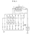
- the Group III organometallic halide vapors are supplied to the reactor from the gas panel through entry port 1 and the group V source vapors are supplied through entry port 2.
- the gas panel is the same as is used in cold wall reactors and described in Kuech, Material Science Reports V 2, 1987 page 6, incorporated herein by reference.
- the corresponding group III organometallic compounds are supplied to the reactor through entry port 1 via one of more of lines 4, 5 and 6. If only one group III element is in the semiconductor compound then one line is used whereas if two or three group III elements are in the semiconductor compound then two or three lines, respectively, are used to supply the different group III organometallic compounds.
- the corresponding group V sources are supplied to the reactor through entry port 2 via lines 7 and 8.
- the reactor consists of a quartz tube 9 in a furnace 10. At higher pressures a throttled mechanical pump is adequate whereas at lower pressures a turbo-molecular pump is more suitable.
- Volatizable elemental Group V compounds or Group V hydrides are used as the source of the Group V atom to form the III-V semiconductor compound.
- a plurality of vapor flows are introduced into the reaction chamber including a Group III organometallic halide vapor having a mole fraction in the range of .5 to 10 ⁇ 3 and a Group V source vapor having a mole fraction in the range of .5 to 10 ⁇ 3.
- the reaction chamber is heated and the Group III organometallic halide vapor dissociates to form a metal halide vapor which chemically reacts with the Group V compound vapor to form the epitaxial layer.
- the thickness of the epitaxial layers so produced depends upon the growth rate and the time of deposition which are in turn generally controlled by the temperature, reactor pressure and mole fraction of the reactants.
- the hot-wall reactor is operated at very low pressures, less than 13.33 mbar, preferably in the range 1.33 ⁇ bar to 13.33 mbar.
- the low pressure conditions enhances the mass transport of growth nutrients to the surface.
- the rate limiting step to growth will be a temperature dependent reaction.
- the low pressure also provides rapid transport of the growth constituents to the growth surface.
- the combination of low pressure and a hot wall system allows for the high density stacking of the substrates into the hot wall reactor and a highly uniform growth of the deposition over the entire substrate surface. In the present invention, batch processing of wafers can be achieved with excellent uniformity of deposition, both on a wafer and from wafer to wafer.
- batch processing may be achieved in the present system by vertical stacking of a large quantity of wafers as shown at 11 in Figure 1.
- Such an arrangement allows for a small interwafer spacing on the order of 1-10 millimeters.
- a high throughput of epitaxial growth is obtained by use of the described class of precursors in a hot wall reactor at very low pressures.
- Alloy compound semiconductor structures may be grown using the method of the invention in which there is a single metal atom M and a single Group V element, such as GaAs, InP and AlAs.
- Alloy compound semiconductors having multiple Group III metal atoms may also be grown by introducing a plurality of organometallic precursors into the system.
- the growth of compound semiconductors having two Group III metal atoms, such as, Al x Ga 1-x As where 0 ⁇ x ⁇ 1 is accomplished through the introduction of both a Ga and an Al bearing organometallic halide precursor such as Diethyl Gallium Chloride and Dimethyl Aluminum Chloride.
- the growth of AlGaP is similarly accomplished by substituting P for As as the Group V atom.
- three Group III organometallic halide precursors can be provided to form a compound semiconductor having three Group III metal atoms, such as, (Al x Ga 1-x ) y In 1-y P where x is in the range 0 ⁇ x ⁇ 1 and y is in the range of 0 ⁇ y ⁇ 1.
- Semiconductor compounds containing two different Group III elements and two different Group V elements are formed by providing two different Group III organometallic compounds and two different group V sources.
- a III-V compound of this form is In x Ga 1-x As y P 1-y where x is in the range 0 ⁇ x ⁇ 1 and y is in the range 0 ⁇ y ⁇ 1.
- the Group III-V compound may be made by introducing the appropriate precursors.
- the process of the invention has further application to the growth of heterojunctions through a change in the composition of the gases inputted to the growth reactor.
- the low pressure operation of the reactor allows for the rapid exchange of gases in the reactor tube and hence a sharp transition in the composition of the deposited films.
- changes on the anion sublattice are effected.
- heterojunctions of for example, AlGaAs/GaAs on a GaAs substrate may be formed in-situ by first epitaxially grown GaAs in a first step and then epitaxially growing AlGaAs in a second step by adding the Al bearing precursor.
- In-situ doping is possible by introducing dopant source gases through entry port 3 at the time of introduction of the Group III and Group V source gases, or during interruptions in the epitaxial deposition.
- N and P type doping is accomplished through the controlled introduction of conventional gas compounds such as silane, disilane, dimethyl zinc or other Group IIB, IV or VI compounds.
- the dopant incorporation into the growing film is dependent on temperature and pressure.
- the hot wall reactor operated at very low pressures results in a highly uniform incorporation of doped material.
- the precursors of the invention provide selective epitaxial growth of Group III-V compounds on a masked substrate in an MOVPE system.
- a gaseous mixture including at least one organometallic halide compound of a Group III metal and at least one compound of a Group V element under suitable conditions of temperature and pressure are introduced into a MOVPE reaction chamber having a masked substrate to selectively deposit on the unmasked areas of the substrate an epitaxial layer of a III-V compound semiconductor.
- a metal mono-halgen such as GaCl.
- Such mono-halogen compounds have a strong metal-halogen bond that allows for the decomposition of the compound to a stable entity instead of free metal.
- the chemical entity does not react on the masking material until very high supersaturations are achieved.
- the nucleation of polycrystalline material is strongly suppressed.
- Masking materials are SiO2, SiN x , SiON x , Al2O3 and AlN.
- the free halogen in the growth environment acts to etch and remove any small embryonic crystals from the mask surface before a critical nuclei can be formed. These compounds react to form mono-halogen precursors in the gas phase which possess a high vapor pressure and do not adsorb strongly on masking surfaces at typical MOVPE growth temperatures.
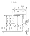
- the cold wall system is a flow system in which the source gases are introduced into the reactor chamber having pumps located on the reaction chamber to maintain the operating pressure.
- the pressure is determined by the amount and flow of the gas species.
- the temperature is typically in the range of 500 to 800°C and the pressure is typically in the range of 1.33 mbar to 1.013 bar.
- a plurality of vapor flows is introduced into the reaction chamber including a Group III organometallic halide vapor having a mole fraction in the range of 10 ⁇ 3 to 10 ⁇ 4 and a Group V source vapor having a mole fraction in the range of 5 to 1000 times greater than the Group III organometallic halide vapor.
- the source of heat in the cold wall system may be for example radiant energy or rf induction to heat the reaction chamber to the growth temperature.
- heating is provided to vessel 12 by rf heating coil 13.
- the growth chemistry in the cold wall system, as in the hot wall is controlled by the temperature, reactor pressure and mole fraction of reactants.
- the use of at least one of the precursors of the invention enables selective epitaxy without complicated edge morphologies due to the diffusion of growth species from the mask surface to the edge of the growing film. No deposition is seen on the mask. Only high quality Group III-V compounds are deposited in the unmasked areas.
- the semiconductor materials that can be selectively deposited include any combination of one or more Group III elements of Al, Ga and In and one or more Group V elements of As, P and Sb.
- any of the particular compounds described earlier with respect to epitaxial growth on the hot wall, low pressure system may be selectively deposited on a masked substrate.
Landscapes
- Chemical & Material Sciences (AREA)
- Engineering & Computer Science (AREA)
- Crystallography & Structural Chemistry (AREA)
- Materials Engineering (AREA)
- Metallurgy (AREA)
- Organic Chemistry (AREA)
- Inorganic Chemistry (AREA)
- Chemical Kinetics & Catalysis (AREA)
- General Chemical & Material Sciences (AREA)
- Crystals, And After-Treatments Of Crystals (AREA)
Applications Claiming Priority (2)
| Application Number | Priority Date | Filing Date | Title |
|---|---|---|---|
| US21518188A | 1988-07-05 | 1988-07-05 | |
| US215181 | 1988-07-05 |
Publications (2)
| Publication Number | Publication Date |
|---|---|
| EP0349781A2 true EP0349781A2 (fr) | 1990-01-10 |
| EP0349781A3 EP0349781A3 (fr) | 1991-01-09 |
Family
ID=22801996
Family Applications (1)
| Application Number | Title | Priority Date | Filing Date |
|---|---|---|---|
| EP19890110333 Withdrawn EP0349781A3 (fr) | 1988-07-05 | 1989-06-08 | Croissance épitaxiale de composés III-V par la déposition à partir de vapeurs métalorganiques |
Country Status (4)
| Country | Link |
|---|---|
| EP (1) | EP0349781A3 (fr) |
| JP (1) | JPH0239423A (fr) |
| BR (1) | BR8903288A (fr) |
| CA (1) | CA1313343C (fr) |
Cited By (2)
| Publication number | Priority date | Publication date | Assignee | Title |
|---|---|---|---|---|
| EP0524817A3 (en) * | 1991-07-23 | 1993-08-18 | Nec Corporation | Crystal growth method of iii - v compound semiconductor |
| DE4143472C2 (de) * | 1990-04-13 | 1995-10-26 | Mitsubishi Electric Corp | Verfahren zur Herstellung einer Halbleitereinrichtung |
Families Citing this family (1)
| Publication number | Priority date | Publication date | Assignee | Title |
|---|---|---|---|---|
| JP2753276B2 (ja) * | 1988-09-21 | 1998-05-18 | 株式会社日立製作所 | 半導体薄膜の気相成長法 |
Family Cites Families (1)
| Publication number | Priority date | Publication date | Assignee | Title |
|---|---|---|---|---|
| US4147571A (en) * | 1977-07-11 | 1979-04-03 | Hewlett-Packard Company | Method for vapor epitaxial deposition of III/V materials utilizing organometallic compounds and a halogen or halide in a hot wall system |
-
1989
- 1989-05-25 CA CA000600746A patent/CA1313343C/fr not_active Expired - Fee Related
- 1989-06-08 EP EP19890110333 patent/EP0349781A3/fr not_active Withdrawn
- 1989-06-20 JP JP15598189A patent/JPH0239423A/ja active Pending
- 1989-07-04 BR BR8903288A patent/BR8903288A/pt unknown
Cited By (3)
| Publication number | Priority date | Publication date | Assignee | Title |
|---|---|---|---|---|
| DE4143472C2 (de) * | 1990-04-13 | 1995-10-26 | Mitsubishi Electric Corp | Verfahren zur Herstellung einer Halbleitereinrichtung |
| EP0524817A3 (en) * | 1991-07-23 | 1993-08-18 | Nec Corporation | Crystal growth method of iii - v compound semiconductor |
| US5294565A (en) * | 1991-07-23 | 1994-03-15 | Nec Corporation | Crystal growth method of III - V compound semiconductor |
Also Published As
| Publication number | Publication date |
|---|---|
| CA1313343C (fr) | 1993-02-02 |
| BR8903288A (pt) | 1990-02-13 |
| JPH0239423A (ja) | 1990-02-08 |
| EP0349781A3 (fr) | 1991-01-09 |
Similar Documents
| Publication | Publication Date | Title |
|---|---|---|
| EP1432844B1 (fr) | Appareil pour depot chimique en phase vapeur inverse | |
| KR102385703B1 (ko) | 그래핀 층 구조체를 제조하는 방법 | |
| US5124278A (en) | Amino replacements for arsine, antimony and phosphine | |
| US4147571A (en) | Method for vapor epitaxial deposition of III/V materials utilizing organometallic compounds and a halogen or halide in a hot wall system | |
| US4368098A (en) | Epitaxial composite and method of making | |
| US4404265A (en) | Epitaxial composite and method of making | |
| US3922475A (en) | Process for producing nitride films | |
| US4904616A (en) | Method of depositing arsine, antimony and phosphine substitutes | |
| JP2006140450A (ja) | 有機金属化合物 | |
| US5036022A (en) | Metal organic vapor phase epitaxial growth of group III-V semiconductor materials | |
| US3394390A (en) | Method for making compond semiconductor materials | |
| Tsang | Chemical beam epitaxy of InGaAs | |
| US4988640A (en) | Method of doping and implanting using arsine, antimony, and phosphine substitutes | |
| US3338761A (en) | Method and apparatus for making compound materials | |
| CA1313343C (fr) | Methode de croissance epitaxiale en phase gazeuse de melanges organo-metalliques pour semiconducteurs de groupe iii-v | |
| JPH0654764B2 (ja) | 半絶縁性ガリウムヒ素形成方法 | |
| US4895737A (en) | Metal-organic chemical vapor deposition | |
| JPH09171966A (ja) | 化合物半導体へのn型ドーピング方法およびこれを用いた化学ビーム堆積方法、有機金属分子線エピタキシャル成長方法、ガスソース分子線エピタキシャル成長方法、有機金属化学気相堆積方法および分子線エピタキシャル成長方法並びにこれらの結晶成長方法によって形成された化合物半導体結晶およびこの化合物半導体結晶によって構成された電子デバイスおよび光デバイス | |
| JPS60169563A (ja) | テルル化金属の製造方法及び装置 | |
| JPS6136371B2 (fr) | ||
| CA1322935C (fr) | Composes ramifies monoalkyliques du groupe va, utilises comme source d'elements mocvd | |
| JPS58223317A (ja) | 化合物半導体結晶成長法及びその装置 | |
| JP2736417B2 (ja) | 半導体素子の製法 | |
| WO1986002776A1 (fr) | Technique de developpement de films epitaxiaux semiconducteurs composites | |
| JPH0760800B2 (ja) | 化合物半導体の気相成長法 |
Legal Events
| Date | Code | Title | Description |
|---|---|---|---|
| PUAI | Public reference made under article 153(3) epc to a published international application that has entered the european phase |
Free format text: ORIGINAL CODE: 0009012 |
|
| AK | Designated contracting states |
Kind code of ref document: A2 Designated state(s): CH DE ES FR GB IT LI NL SE |
|
| 17P | Request for examination filed |
Effective date: 19900512 |
|
| PUAL | Search report despatched |
Free format text: ORIGINAL CODE: 0009013 |
|
| AK | Designated contracting states |
Kind code of ref document: A3 Designated state(s): CH DE ES FR GB IT LI NL SE |
|
| 17Q | First examination report despatched |
Effective date: 19920513 |
|
| STAA | Information on the status of an ep patent application or granted ep patent |
Free format text: STATUS: THE APPLICATION IS DEEMED TO BE WITHDRAWN |
|
| 18D | Application deemed to be withdrawn |
Effective date: 19921124 |