EP0350155A2 - Digitale Verstärkungsregelungsstufe - Google Patents
Digitale Verstärkungsregelungsstufe Download PDFInfo
- Publication number
- EP0350155A2 EP0350155A2 EP89304834A EP89304834A EP0350155A2 EP 0350155 A2 EP0350155 A2 EP 0350155A2 EP 89304834 A EP89304834 A EP 89304834A EP 89304834 A EP89304834 A EP 89304834A EP 0350155 A2 EP0350155 A2 EP 0350155A2
- Authority
- EP
- European Patent Office
- Prior art keywords
- conductors
- currents
- transistor
- differential amplifier
- signals
- Prior art date
- Legal status (The legal status is an assumption and is not a legal conclusion. Google has not performed a legal analysis and makes no representation as to the accuracy of the status listed.)
- Withdrawn
Links
Images
Classifications
-
- H—ELECTRICITY
- H03—ELECTRONIC CIRCUITRY
- H03G—CONTROL OF AMPLIFICATION
- H03G3/00—Gain control in amplifiers or frequency changers
- H03G3/001—Digital control of analog signals
-
- H—ELECTRICITY
- H03—ELECTRONIC CIRCUITRY
- H03G—CONTROL OF AMPLIFICATION
- H03G1/00—Details of arrangements for controlling amplification
- H03G1/0005—Circuits characterised by the type of controlling devices operated by a controlling current or voltage signal
- H03G1/0017—Circuits characterised by the type of controlling devices operated by a controlling current or voltage signal the device being at least one of the amplifying solid-state elements
- H03G1/0023—Circuits characterised by the type of controlling devices operated by a controlling current or voltage signal the device being at least one of the amplifying solid-state elements in emitter-coupled or cascode amplifiers
Definitions
- This invention relates to differential amplifiers, and more particularly, it relates to a controller responsive to a digital signal for varying the outputs of a differential amplifier.
- the present invention provides a controller for a differential multiplier which uses less power, is simpler in structure, and relatively insensitive to power supply variations. In addition, because the gain is dependent only upon currents I1 and I2, the gain accuracy of the circuit is much improved over standard Gilbert multiplier implementations.
- a differential amplifier is responsive to first and second control signals for generating from an input signal first and second output signals, respectively.
- the controller of the present invention generates a digital signal representative of a desired relationship between the first and second output signals.
- the digital signal is converted into the first and second control signals such that the desired relationship between the first and second output signals results from applying the control signals to the differential amplifier.
- the digital signal is converted by a digital to analog converter (DAC) for converting the digital signal into a pair of analog signals.
- the DAC outputs the analog signals as currents on a pair of conductors, with the sum of the currents being a constant and the relative magnitudes of the currents being determined by the digital signal.
- Means are provided for maintaining the voltages of the conductors carrying the analog signals at a common level for preferred operation of the DAC.
- Differential amplifiers are useful in a variety of situations which require amplification or multiplication of signals.
- the present invention was developed for manually controlling a signal input to an oscilloscope. For each knob position a unique digital signal is generated for controlling the scope image. Appropriate knob positions also provide for inverting the signal. Thus, the viewed signal image can take a range of ⁇ 1 times the input signal. It will be appreciated however that the invention has applicability to a variety of applications.
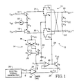
- Amplifier 10 includes a differential amplification circuit 12, also referred to as a Gilbert gain cell, and a controller 14.
- Circuit 12 has a pair of input terminals 16 and 18 across which a differential input voltage V in is applied. These voltages are fed to the bases of transistors Q1 and Q2, respectively. These transistors have currents the sum of which are determined by current source 20 which feeds through resistors R1 and R2.
- the current passing through transistors Q1 and Q2 also passes through respective pairs of differentially connected transistor pairs Q3/Q4 and Q5/Q6, as shown, via conductors 21 and 22.
- the collectors of transistors Q3 and Q6 are connected to an output conductor 23, and the collectors of transistors Q4 and Q5 are connected to an output conductor 24.
- Conductors 23 and 24 carry respective output voltages V out ⁇ and V out + which form the differential output voltage V out .
- Conductors 23 and 24 are also connected to voltage source V cc through resistors R3 and R4, respectively.
- Circuit 12 forms a conventional Gilbert multiplier circuit.
- the maximum gain is set by the ratio of resistors R 1,2 to resistors R 3,4 .
- the bases of transistors Q3 and Q5 and of transistors Q4 and Q6 are tied together, respectively, by conductors 26 and 28.
- the actual gain of circuit 12 is proportional to the differential currents on conductors 26 and 28. Controller 14 establishes the currents on these conductors.
- Controller 14 includes a digital signal generator 30, such as the manually adjustable oscilloscope knob discussed previously.
- Generator 30 outputs one byte of digital data which is representative of a desired relationship of the output signals on conductors 23 and 24. This data is fed into a CMOS DAC 32 which then generates analog currents on conductors 34 and 36 corresponding to the digital signal input to it. Because the gain cell is controlled by the difference over the sum of currents I1 and I2, the value and stability of the reference voltage, V ref , are not critical.
- V1 and V2 on conductors 34 and 36 need to be kept at virtual ground.
- Voltage V1 is maintained at virtual ground by the use of npn transistors Q7 and Q8 which have their bases connected together and to conductor 28.
- a current mirror 38 provides equal currents for these two transistors.
- the emitter of transistor Q7 is grounded.
- the base-to-emitter voltages of these transistors are equal. This forces V1 to be at 0 volts.
- the current mirror consists of pnp transistors Q10 and Q11 which are connected to a power supply having voltage V cc .
- the bases of these transistors are connected and also connected to the collector of transistor Q10.
- the collectors of transistors Q7 and Q8 are respectively connected to the collectors of transistors Q10 and Q11, as shown.
- the collector and base of transistor Q7 are shorted.
- This current mirror arrangement has two stable operating points, one of which is characterized by zero current flow in transistor Q8.
- a diode D12 assures that this is avoided, particularly at startup.
- the diode is connected between conductor 28 and ground with the cathode connected to conductor 28. As the voltage on conductor 28 decreases sufficiently, the diode becomes forward biased and begins to conduct. This maintains a minimum voltage on conductor 28.
- the current mirror and Q8 then start to conduct. As they do, the voltage on conductor 28 raises and diode D12 becomes reverse biased.
- the voltage on conductor 36 is maintained at virtual ground by the combination of a transistor Q9 and an operational amplifier 40.
- the noninverting input to the op amp is joined to conductor 34.
- the inverting input is joined to conductor 36.
- the output is connected to conductor 26 and to the base of transistor Q9.
- the emitter of transistor Q9 is connected to conductor 36.
- the op amp forces transistor Q9 to operate so that the voltage V2 on conductor 36 is maintained the same as the voltage V1 on conductor 34, i. e., virtual ground.
- the currents which DAC 32 outputs thus do not directly drive the controlled transistors in circuit 12. Rather, the base-emitter voltages of transistors Q8 and Q9, which are a function of currents I1 and I2, form the difference in base-emitter voltages for transistors Q4 and Q6 and of transistors Q3 and Q5, respectively. Operation of the differential amplification circuit 12 is thus controlled by operation of DAC 32.
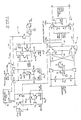
- a partial schematic of differential amplifier 10 is shown. The same components are shown with the same reference numbers.
- This circuit shows the specific circuitry provided in an actual embodiment of the circuit of the invention.
- Conductors 23 and 24 are shown to include inline transistors Q144 and Q145. The bases of these transistors are connected together and to a voltage divider circuit 42. This circuit arrangement is used for impedance matching with a subsequent low impedance circuit and to protect the output section of circuit 12 from changes in voltage at the output.
- Op amp 40 is shown formed of differentially connected transistors Q137, the base of which is the inverting input, and Q138, the base of which is the noninverting input. The output is taken at the emitter of a transistor Q199, as shown.
- the input stage of circuit 12 is similar to the stage shown in Fig. 1, with the exception of an additional set of emitters and resistors for discrete gain switching in Fig. 2. The digital signal generator is omitted for simplicity.
- the present invention provides a differential amplifier which is simple to construct, is relatively insensitive to power supply variations, and inherently uses little power. This is accomplished through the use of a generator for generating a digital signal representative of a desired output current relationship. The digital signal is converted to an analog signal and applied to the control terminals of the differential amplification circuit.
Landscapes
- Control Of Amplification And Gain Control (AREA)
- Amplifiers (AREA)
Applications Claiming Priority (2)
| Application Number | Priority Date | Filing Date | Title |
|---|---|---|---|
| US215964 | 1988-07-07 | ||
| US07/215,964 US4885547A (en) | 1988-07-07 | 1988-07-07 | Gain cell with digital control |
Publications (2)
| Publication Number | Publication Date |
|---|---|
| EP0350155A2 true EP0350155A2 (de) | 1990-01-10 |
| EP0350155A3 EP0350155A3 (de) | 1990-12-27 |
Family
ID=22805107
Family Applications (1)
| Application Number | Title | Priority Date | Filing Date |
|---|---|---|---|
| EP19890304834 Withdrawn EP0350155A3 (de) | 1988-07-07 | 1989-05-12 | Digitale Verstärkungsregelungsstufe |
Country Status (3)
| Country | Link |
|---|---|
| US (1) | US4885547A (de) |
| EP (1) | EP0350155A3 (de) |
| JP (1) | JPH0646689B2 (de) |
Cited By (3)
| Publication number | Priority date | Publication date | Assignee | Title |
|---|---|---|---|---|
| EP0666645B1 (de) * | 1994-02-04 | 1999-10-20 | TEMIC Semiconductor GmbH | Schaltungsanordnung mit einer Verstärkerschaltung mit einstellbarer Verstärkung |
| WO2000003474A3 (en) * | 1998-07-13 | 2000-04-13 | Koninkl Philips Electronics Nv | Converter circuit and variable gain amplifier with temperature compensation |
| FR2798235A1 (fr) * | 1999-09-03 | 2001-03-09 | St Microelectronics Sa | Dispositif amplificateur de puissance a gain controle, en particulier pour des circuits radiofrequence appliques a la telephonie mobile cellulaire |
Families Citing this family (9)
| Publication number | Priority date | Publication date | Assignee | Title |
|---|---|---|---|---|
| US5039952A (en) * | 1990-04-20 | 1991-08-13 | International Business Machines Corp. | Electronic gain cell |
| US5184088A (en) * | 1992-06-10 | 1993-02-02 | Samsung Electronics Co., Ltd. | Controlled-gain transistor amplifier without D-C shift or signal phase reversal in load current |
| US5552881A (en) * | 1994-03-17 | 1996-09-03 | Teradyne, Inc. | Method and apparatus for scanning a fiber optic network |
| US6337648B1 (en) * | 1998-11-25 | 2002-01-08 | Texas Instruments Inc. | MOS transistor digital-to-analog converter |
| US8138851B2 (en) * | 2010-03-16 | 2012-03-20 | Micrel, Inc. | High bandwidth programmable transmission line equalizer |
| US8295336B2 (en) * | 2010-03-16 | 2012-10-23 | Micrel Inc. | High bandwidth programmable transmission line pre-emphasis method and circuit |
| US8379702B2 (en) * | 2010-03-16 | 2013-02-19 | Micrel, Inc. | High bandwidth programmable transmission line pre-emphasis method and circuit |
| US8379701B2 (en) * | 2010-03-16 | 2013-02-19 | Micrel, Inc. | High bandwidth dual programmable transmission line pre-emphasis method and circuit |
| CN102976356B (zh) * | 2012-12-17 | 2015-01-14 | 贵州省化工研究院 | 一种氟硅化合物制备高品质氟化氢铵的方法 |
Family Cites Families (4)
| Publication number | Priority date | Publication date | Assignee | Title |
|---|---|---|---|---|
| US4156283A (en) * | 1972-05-30 | 1979-05-22 | Tektronix, Inc. | Multiplier circuit |
| JPS5541012A (en) * | 1978-09-18 | 1980-03-22 | Hitachi Ltd | Gain control circuit |
| JPS5541013A (en) * | 1978-09-18 | 1980-03-22 | Hitachi Ltd | Gain control circuit |
| JPS566513A (en) * | 1979-06-29 | 1981-01-23 | Matsushita Electric Ind Co Ltd | Signal level control circuit |
-
1988
- 1988-07-07 US US07/215,964 patent/US4885547A/en not_active Expired - Lifetime
-
1989
- 1989-05-12 EP EP19890304834 patent/EP0350155A3/de not_active Withdrawn
- 1989-07-04 JP JP1172858A patent/JPH0646689B2/ja not_active Expired - Fee Related
Cited By (4)
| Publication number | Priority date | Publication date | Assignee | Title |
|---|---|---|---|---|
| EP0666645B1 (de) * | 1994-02-04 | 1999-10-20 | TEMIC Semiconductor GmbH | Schaltungsanordnung mit einer Verstärkerschaltung mit einstellbarer Verstärkung |
| WO2000003474A3 (en) * | 1998-07-13 | 2000-04-13 | Koninkl Philips Electronics Nv | Converter circuit and variable gain amplifier with temperature compensation |
| FR2798235A1 (fr) * | 1999-09-03 | 2001-03-09 | St Microelectronics Sa | Dispositif amplificateur de puissance a gain controle, en particulier pour des circuits radiofrequence appliques a la telephonie mobile cellulaire |
| US6594474B1 (en) | 1999-09-03 | 2003-07-15 | Stmicroelectronics Sa | Controlled-gain power amplifier device, in particular for radio-frequency circuits applied to cellular mobile telephony |
Also Published As
| Publication number | Publication date |
|---|---|
| US4885547A (en) | 1989-12-05 |
| JPH0646689B2 (ja) | 1994-06-15 |
| EP0350155A3 (de) | 1990-12-27 |
| JPH0265514A (ja) | 1990-03-06 |
Similar Documents
| Publication | Publication Date | Title |
|---|---|---|
| EP0350155A2 (de) | Digitale Verstärkungsregelungsstufe | |
| US4663594A (en) | Electronic phase shifter circuit and method | |
| US3921091A (en) | Amplifier circuit | |
| EP0004099A1 (de) | Elektrisch einstellbare Impedanzschaltung | |
| JPH0544845B2 (de) | ||
| US5481180A (en) | PTAT current source | |
| JPS59221014A (ja) | 電圧電流変換回路 | |
| GB2122831A (en) | Voltage to current converting amplifiers | |
| JP3938793B2 (ja) | 擬似対数利得制御を用いる可変利得増幅器 | |
| US4219781A (en) | Transistor amplifier circuit | |
| JP2733962B2 (ja) | 利得制御増幅器 | |
| US4878031A (en) | Class B variable gain control circuit | |
| JP3216134B2 (ja) | 指数的な利得制御を行う増幅回路 | |
| JPS5820482B2 (ja) | 増巾器 | |
| KR920009548B1 (ko) | 전류원 장치 | |
| KR930003522B1 (ko) | 전자증폭제어를 하는 전기신호의 증폭회로 | |
| US4451798A (en) | Gain-controlled amplifier | |
| JPH0462608B2 (de) | ||
| JPH0527282B2 (de) | ||
| KR940003612Y1 (ko) | 오디오증폭기의 출력전압 안정화회로 | |
| JPS5816366B2 (ja) | レベルシフトカイロ | |
| KR830002320B1 (ko) | 신호 가산회로 | |
| JP2781850B2 (ja) | 利得可変増幅回路 | |
| GB2126031A (en) | Cascode amplifier | |
| JP2621573B2 (ja) | 信号抑圧回路 |
Legal Events
| Date | Code | Title | Description |
|---|---|---|---|
| PUAI | Public reference made under article 153(3) epc to a published international application that has entered the european phase |
Free format text: ORIGINAL CODE: 0009012 |
|
| AK | Designated contracting states |
Kind code of ref document: A2 Designated state(s): DE GB NL |
|
| PUAL | Search report despatched |
Free format text: ORIGINAL CODE: 0009013 |
|
| AK | Designated contracting states |
Kind code of ref document: A3 Designated state(s): DE GB NL |
|
| 17P | Request for examination filed |
Effective date: 19910517 |
|
| STAA | Information on the status of an ep patent application or granted ep patent |
Free format text: STATUS: THE APPLICATION HAS BEEN WITHDRAWN |
|
| 18W | Application withdrawn |
Withdrawal date: 19930316 |