EP0350663B1 - Schaltungsanordnung zur Demodulation eines Hilfsträgers - Google Patents
Schaltungsanordnung zur Demodulation eines Hilfsträgers Download PDFInfo
- Publication number
- EP0350663B1 EP0350663B1 EP89111145A EP89111145A EP0350663B1 EP 0350663 B1 EP0350663 B1 EP 0350663B1 EP 89111145 A EP89111145 A EP 89111145A EP 89111145 A EP89111145 A EP 89111145A EP 0350663 B1 EP0350663 B1 EP 0350663B1
- Authority
- EP
- European Patent Office
- Prior art keywords
- signal
- mixing
- mixed
- signals
- case
- Prior art date
- Legal status (The legal status is an assumption and is not a legal conclusion. Google has not performed a legal analysis and makes no representation as to the accuracy of the status listed.)
- Expired - Lifetime
Links
- 238000000034 method Methods 0.000 claims description 12
- 238000001914 filtration Methods 0.000 abstract description 2
- 238000006243 chemical reaction Methods 0.000 abstract 1
- 125000004122 cyclic group Chemical group 0.000 abstract 1
- 238000005070 sampling Methods 0.000 description 10
- 239000000654 additive Substances 0.000 description 3
- 230000000996 additive effect Effects 0.000 description 3
- 230000036039 immunity Effects 0.000 description 2
- 230000033228 biological regulation Effects 0.000 description 1
- 230000015572 biosynthetic process Effects 0.000 description 1
- 239000000969 carrier Substances 0.000 description 1
- 230000000295 complement effect Effects 0.000 description 1
- 238000009795 derivation Methods 0.000 description 1
- 238000011161 development Methods 0.000 description 1
- 230000018109 developmental process Effects 0.000 description 1
- 238000010586 diagram Methods 0.000 description 1
- 239000000203 mixture Substances 0.000 description 1
- 230000005236 sound signal Effects 0.000 description 1
- 230000003595 spectral effect Effects 0.000 description 1
- 230000001629 suppression Effects 0.000 description 1
Images

Classifications
-
- H—ELECTRICITY
- H03—ELECTRONIC CIRCUITRY
- H03D—DEMODULATION OR TRANSFERENCE OF MODULATION FROM ONE CARRIER TO ANOTHER
- H03D1/00—Demodulation of amplitude-modulated oscillations
- H03D1/22—Homodyne or synchrodyne circuits
- H03D1/2245—Homodyne or synchrodyne circuits using two quadrature channels
- H03D1/2254—Homodyne or synchrodyne circuits using two quadrature channels and a phase locked loop
-
- H—ELECTRICITY
- H03—ELECTRONIC CIRCUITRY
- H03B—GENERATION OF OSCILLATIONS, DIRECTLY OR BY FREQUENCY-CHANGING, BY CIRCUITS EMPLOYING ACTIVE ELEMENTS WHICH OPERATE IN A NON-SWITCHING MANNER; GENERATION OF NOISE BY SUCH CIRCUITS
- H03B28/00—Generation of oscillations by methods not covered by groups H03B5/00 - H03B27/00, including modification of the waveform to produce sinusoidal oscillations
-
- H—ELECTRICITY
- H03—ELECTRONIC CIRCUITRY
- H03D—DEMODULATION OR TRANSFERENCE OF MODULATION FROM ONE CARRIER TO ANOTHER
- H03D7/00—Transference of modulation from one carrier to another, e.g. frequency-changing
- H03D7/16—Multiple-frequency-changing
- H03D7/165—Multiple-frequency-changing at least two frequency changers being located in different paths, e.g. in two paths with carriers in quadrature
Definitions
- the invention is based on a method according to the type of the main claim.
- an additive error occurs at the output.
- This error can occur in particular in the case of a useful signal, such as the subcarrier of the traffic radio system and the radio data system (RDS).
- the object of the invention is to provide a method for demodulating an auxiliary carrier, in which digital further processing of the useful signal is possible without an additive error occurring. Furthermore, since stronger interference signals such as audio signals and the stereopilot sound occur in connection with the subcarrier in addition, interference immunity of the circuit, in particular suppression of image frequencies, is required.
- the method according to the invention with the characterizing features of the main claim has the advantage that digital further processing of the useful signal is possible, practically no additive error occurs and that there is a sufficiently high level of interference immunity.
- the method according to the invention can be implemented with little effort and is suitable for an integrated circuit.
- EP-A-0 156 701 discloses an analog frequency shift into the baseband, a subsequent digitization, and the formation of two signals in quadrature by means of registers, complementary formers and multiplexers.
- two mixed signals with a phase difference of 90 ° are generated.
- a derivation of both quadrature components is possible in a simple manner by scanning the mixed products four times.
- the invention also includes the generation of more than two mixed signals with corresponding phase differences and a more frequent sampling of the mixed products. In the case of an even number of mixed signals, sampling values for both quadrature components are readily available.
- quadrature components can also be derived in the case of an odd number of mixed signals, one being able to be obtained directly and the other by interpolation between two samples.
- the circuit arrangement according to FIG. 1 is supplied with the signal to be demodulated at 11. It follows the relationship A (t) * sin ( ⁇ t + ⁇ ).
- a (t) is the modulation signal, while ⁇ and ⁇ stand, as usual, for the angular frequency and the phase position of the carrier.
- the RDS and traffic radio subcarrier has a frequency of 57 kHz.
- the mixers 12, 13 are each supplied with a mixed signal, the frequency of which is 61.75 kHz. It is generated in a digitally controllable oscillator 14 and a subsequent frequency divider 31 in two phase positions different from one another by 90 ° by frequency division of a signal with four times the frequency of the mixed signals.
- Subsequent low-pass filters 15, 16 suppress spectral components above the useful frequency range.
- the output signals of the low-pass filters 15, 16 then result in A (t) * cos (( ⁇ o - ⁇ 57 ) t + ⁇ ) or A (t) * sin (( ⁇ o - ⁇ 57 ) t + ⁇ ).
- the mixture does not yet convert the modulation signal A (t) into the baseband, but rather only modulated carriers with a frequency of 4.75 kHz are created.
- Both signals which are called intermediate frequency signals in the following, are each fed to an analog / digital converter 17, 18, a clock frequency of 19 kHz being provided by dividing the frequency of the oscillator 14 by 13 with the aid of a Frequency divider 19 is generated and samples the intermediate frequency signals four times per period.
- the outputs of the analog / digital converters 17, 18 are followed by two channels I and II, each of which has a controllable changeover switch 20, 21, a signal inverter 22, 23, a further controllable changeover switch 24, 25 and a low-pass filter 26, 27 be formed.
- the output signal of the low-pass filter 26 can be taken from an output 28, while the output signal of the low-pass filter 27 is used in the exemplary embodiment shown to control the digitally controllable oscillator 14.
- the switches 20, 21, 24, 25 are controlled via two further frequency dividers 29, 30 in such a way that in channel I a sampling takes place at 0 ° and 180 ° in relation to a period of the intermediate frequency signal, while in channel II at 90 ° and 270 ° is scanned. Every second sample value is inverted with the aid of the circuits 22, 23, so that demodulation into the baseband takes place. After filtering out carrier residues with the aid of the low-pass filters 26, 27, the demodulated signals are available.
- the signal at the output 28 corresponds to the cosine component of the modulation signal, while a sine component is available at the output of the low-pass filter 27, which is used for regulation in the exemplary embodiment shown.
- n means the ordinal number of the respective scan, + or - whether a signal inversion takes place and und (n) the respective angle of the scan in general form and with 0 as the initial value.
- Fig. 1 the positions of the changeover switch are marked with the values for n, in which the respective position is assumed.
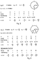
- the table according to FIG. 2 shows that the samples are taken alternately from channel I and channel II. Two consecutive samples are forwarded with the same sign, so that every second half-wave of the intermediate frequency signal is inverted. Through this inversion, any offset error that may be present during the scanning of one of the channels I or II is alternately inverted and not inverted. The offset error is thus converted into a frequency of 4.75 kHz, which is suppressed by the subsequent low-pass filter 26 or 27.
- FIG. 2 also shows a graphical representation of the sampling times 0, 1, 2, 3 and the intermediate frequency signals, the signal of channel I leading that of channel II by 90 °.
- the sampling frequency fs 19 kHz.
- the sampling frequency means the frequency with which the output signals of the analog / digital converters or downstream filters are processed further.
- the table according to FIG. 3 explains an exemplary embodiment with three channels.
- the phase differences are each ⁇ / 3.
- the sampling frequency fs is six times the intermediate frequency, which corresponds to a sampling frequency of 28.5 kHz at an intermediate frequency of 4.75 kHz.
- the intermediate frequency signals are shown in the pie chart of FIG. 3, which also shows the six sampling times 0 to 5.
- the table according to FIG. 3 lists the channel to be scanned, the sign and the angle of the scan for both orthogonal components for the sampling times.
Landscapes
- Engineering & Computer Science (AREA)
- Power Engineering (AREA)
- Digital Transmission Methods That Use Modulated Carrier Waves (AREA)
- Circuits Of Receivers In General (AREA)
- Stereo-Broadcasting Methods (AREA)
- Superheterodyne Receivers (AREA)
Description
- Die Erfindung geht aus von einem Verfahren nach der Gattung des Hauptanspruchs.
- Bei der Amplitudendemodulation und Digitalisierung eines schwachen Nutzsignals mit einer bekannten Anordnung, die aus einem Mischer, einem Tiefpaß und einem Analog/Digital-Wandler besteht, tritt am Ausgang ein additiver Fehler auf. Insbesondere bei einem Nutzsignal, wie beispielsweise dem Hilfsträger des Verkehrsfunksystems und des Radiodatensystems (RDS) kann dieser Fehler auftreten.
- Aufgabe der Erfindung ist es, ein Verfahren zur Demodulation eines Hilfsträgers anzugeben, bei welcher eine digitale Weiterverarbeitung des Nutzsignals möglich ist, ohne daß ein additiver Fehler auftritt. Da ferner im Zusammenhang mit dem Hilfsträger stärkere Störsignale wie beispielsweise Audiosignale und der Stereopilot-Ton auftreten, ist außerdem eine Störsicherheit der Schaltung, insbesondere eine Unterdrückung von Spiegelfrequenzen erforderlich.
- Das erfindungsgemäße Verfahren mit den kennzeichnenden Merkmalen des Hauptanspruchs hat den Vorteil, daß eine digitale Weiterverarbeitung des Nutzsignals möglich ist, praktisch kein additiver Fehler auftritt und daß eine genügend große Störsicherheit vorliegt. Außerdem läßt sich das erfindungsgemäße Verfahren mit geringem Aufwand realisieren und ist für eine integrierte Schaltung geeignet.
- Als Mischsignale eignen sich unter anderem Rechtecksignale und sogenannte Tristate-Signale. Letztere haben den Vorteil, daß sie bei geeigneter Wahl der Tastverhältnisse keine dritte Oberwelle enthalten, weshalb im Nutzband keine Mischprodukte der Frequenzen um 3 ωo

- Da das erfindungsgemäße Verfahren an die Geschwindigkeit der Analog/Digital-Wandler nur geringe Anforderung stellt, lassen sich einfache, gut integrierbare Analog/Digital-Wandler (beispielsweise Delta-Wandler oder Sigma-Delta-Wandler) verwenden, die im Niederfrequenzbereich eine große Dynamik der zu wandelnden Signale gestatten.
- An sich ist aus der EP-A-0 156 701 eine analoge Frequenzverschiebung in das Basisband, eine anschließende Digitalisierung, und die Bildung zweier in Quadratur stehenden Signale, mittels Register, Komplementärbildner und Multiplexer bekannt.
- Durch die in den Unteransprüchen aufgeführten Maßnahmen sind vorteilhafte Weiterbildungen und Verbesserungen der im Hauptanspruch angegebenen Erfindung möglich.
- Bei einer bevorzugten Ausführungsform des erfindungsgemäßen Verfahrens werden zwei Mischsignale mit einem Phasenunterschied von 90° erzeugt. Durch eine viermalige Abtastung pro Periode der Mischprodukte ist eine Ableitung beider Quadraturkomponenten in einfacher Weise möglich. Die Erfindung umfaßt jedoch auch die Erzeugung von mehr als zwei Mischsignalen mit entsprechenden Phasenunterschieden und eine häufigere Abtastung der Mischprodukte. Dabei stehen bei einer geraden Anzahl von Mischsignalen ohne weiteres Abtastwerte für beide Quadraturkomponenten zur Verfügung. Es lassen sich jedoch auch bei einer ungeraden Anzahl von Mischsignalen Quadraturkomponenten ableiten, wobei die eine direkt und die andere durch Interpolation zwischen zwei Abtastwerten gewonnen werden kann.
- Ausführungsbeispiele der Erfindung sind in der Zeichnung anhand mehrerer Figuren dargestellt und in der nachfolgenden Beschreibung näher erläutert. Es zeigt:
- Fig. 1
- ein Blockschaltbild eines Ausführungsbeispiels,
- Fig. 2
- eine tabellarische Darstellung der Funktion der Anordnung nach Fig. 1 und
- Fig. 3
- eine tabellarische Darstellung zur Erläuterung einer erfindungsgemäßen Schaltungsanordnung mit drei Mischsignalen.
- Der Schaltungsanordnung nach Fig. 1 wird bei 11 das zu demodulierende Signal zugeführt. Es folgt der Beziehung A(t) * sin(ωt + ϕ ). Dabei ist A(t) das Modulationssignal, während ω und ϕ wie üblich für die Kreisfrequenz und die Phasenlage des Trägers stehen.
- Der RDS- und Verkehrsfunk-Hilfsträger weist eine Frequenz von 57 KHz auf. Den Mischern 12, 13 wird je ein Mischsignal zugeführt, dessen Frequenz 61,75 KHz beträgt. Es wird in einem digital steuerbaren Oszillator 14 und einem anschließenden Frequenzteiler 31 in zwei um 90° voneinander verschiedenen Phasenlagen durch Frequenzteilung eines Signals mit vierfacher Frequenz der Mischsignale erzeugt.
- Durch anschließende Tiefpaßfilter 15, 16 werden Spektralanteile oberhalb des Nutzfrequenzbereichs unterdrückt. Die Ausgangssignale der Tiefpaßfilter 15, 16 ergeben sich dann zu A(t) * cos((ωo - ω57)t + ϕ ) bzw. A(t) * sin((ωo - ω57)t + ϕ). Durch die Mischung wird das Modulationssignal A(t) noch nicht in das Basisband umgesetzt, sondern es entstehen lediglich modulierte Träger mit der Frequenz von 4,75 KHz.
- Beide Signale, die im folgenden Zwischenfrequenzsignale genannt werden, werden je einem Analog/Digital-Wandler 17, 18 zugeführt, wobei eine Taktfrequenz von 19 KHz vorgesehen ist, die durch Teilung der Frequenz des Oszillators 14 durch 13 mit Hilfe eines Frequenzteilers 19 erzeugt wird und die Zwischenfrequenzsignale jeweils viermal je Periode abtastet.
- An die Ausgänge der Analog/Digital-Wandler 17, 18 schließen sich zwei Kanäle I und II an, die jeweils von einem steuerbaren Umschalter 20, 21, einem Signalinvertierer 22, 23, einem weiteren steuerbaren Umschalter 24, 25 und einem Tiefpaßfilter 26, 27 gebildet werden. Das Ausgangssignal des Tiefpaßfilters 26 kann einem Ausgang 28 entnommen werden, während das Ausgangssignal des Tiefpaßfilters 27 bei dem dargestellten Ausführungsbeispiel zur Steuerung des digital steuerbaren Oszillators 14 verwendet wird.
- Über zwei weitere Frequenzteiler 29, 30 werden die Schalter 20, 21, 24, 25 derart gesteuert, daß im Kanal I jeweils eine Abtastung bei 0° und 180° bezogen auf eine Periode des Zwischenfrequenzsignals erfolgt, während im Kanal II bei 90° und 270° abgetastet wird. Jeder zweite Abtastwert wird mit Hilfe der Schaltungen 22, 23 invertiert, so daß eine Demodulation in das Basisband erfolgt. Nach einem Ausfiltern von Trägerresten mit Hilfe der Tiefpaßfilter 26, 27 stehen die demodulierten Signale zur Verfügung. Dabei entspricht das Signal am Ausgang 28 der Cosinus-Komponente des Modulationssignals, während am Ausgang des Tiefpaßfilters 27 eine Sinus-Komponente zur Verfügung steht, die bei dem dargestellten Ausführungsbeispiel zur Regelung benutzt wird.
- Die Steuerung der Umschalter mit Hilfe der Frequenzteiler 29, 30 wird im folgenden anhand von Fig. 2 näher erläutert. Dabei bedeutet n die Ordnungszahl der jeweiligen Abtastung, + oder - ob eine Signalinvertierung stattfindet und ϕ (n) der jeweilige Winkel der Abtastung in allgemeiner Form und mit 0 als Anfangswert. In Fig. 1 sind die Stellungen der Umschalter mit den Werten für n gekennzeichnet, bei denen die jeweilige Stellung eingenommen wird. So befindet sich beispielsweise der Umschalter 20 bei n = 0 und bei n = 2 im oberen und bei n = 1 und bei n = 3 in der unteren Stellung.
- Der Tabelle gemäß Fig. 2 kann entnommen werden, daß die Abtastwerte abwechselnd aus dem Kanal I und dem Kanal II entnommen werden. Jeweils zwei aufeinanderfolgende Abtastwerte werden mit gleichem Vorzeichen weitergeleitet, so daß jede zweite Halbwelle des Zwischenfrequenzsignals invertiert wird. Durch diese Invertierung wird ein gegebenenfalls vorhandener Offsetfehler bei der Abtastung jeweils eines der Kanäle I oder II abwechselnd invertiert und nicht invertiert. Der Offsetfehler wird somit in eine Frequenz von 4,75 kHz umgesetzt, die von dem anschließenden Tiefpaßfilter 26 bzw. 27 unterdrückt wird.
- Die in Fig. 2 dargestellte Tabelle gilt für eines der Ausgangssignale, während das andere Ausgangssignal durch Vertauschung der Kanäle I und II und durch eine Invertierung bei n = 0, 3, 4, 7, 8 usw. erfolgt. Außer der Tabelle zeigt Fig. 2 noch als graphische Darstellung die Abtastzeitpunkte 0, 1, 2, 3 und die Zwischenfrequenzsignale, wobei das Signal des Kanals I demjenigen des Kanals II um 90° voreilt.
- Bei dem der Tabelle nach Fig. 2 zugrundeliegenden Ausführungsbeispiel beträgt die Abtastfrequenz fs = 19 kHz. In diesem Zusammenhang bedeutet Abtastfrequenz diejenige Frequenz, mit der die Ausgangssignale der Analog/Digital-Wandler bzw. nachgeschalteter Filter weiterverarbeitet werden.
- Während bei dem im Zusammenhang mit den Figuren 1 und 2 erläuterten Ausführungsbeispiel zwei Kanäle vorgesehen sind, erläutert die Tabelle gemäß Fig. 3 ein Ausführungsbeispiel mit drei Kanälen. Dabei betragen die Phasenunterschiede jeweils π/3. Die Abtastfrequenz fs beträgt das Sechsfache der Zwischenfrequenz, was bei einer Zwischenfrequenz von 4,75 kHz einer Abtastfrequenz von 28,5 kHz entspricht. Die Zwischenfrequenzsignale sind in dem Kreisdiagramm gemäß Fig. 3 dargestellt, das ferner die sechs Abtastzeitpunkte 0 bis 5 zeigt. In der Tabelle gemäß Fig. 3 sind für die Abtastzeitpunkte der jeweils abzutastende Kanal, das Vorzeichen und der Winkel der Abtastung für beide orthogonalen Komponenten aufgeführt.
Claims (6)
- Verfahren zur Demodulation eines analogen Trägersignales, insbesondere bei einem Radiodatensystem, wobei zur Bildung eines Ausgangssignals ein Trägersignal mit einem Mischsignal gemischt wird, anschließend gefiltert und digitalisiert wird, dadurch gekennzeichnet, daß das Trägersignal mit mindestens einem zweiten Mischsignal gemischt wird, daß das erste und das zweite Mischsignal gegeneinander phasenverschoben sind und eine vorgegebene Frequenz aufweisen, die außerhalb des Nutzbandes des Trägersignales liegt, daß durch die Mischung des Trägersignals mit den zwei Mischsignalen zwei Mischprodukte erhalten werden, daß daraufhin Frequenzen über dem Nutzfrequenzbereich der Mischprodukte aus den Mischprodukten herausgefiltert werden und die gefilterten Mischprodukte digital gewandelt werden, daß anschließend die digitalen Mischprodukte jeweils zweimal pro Periode zu vorgegebenen Zeitpunkten abgetastet werden, daß die Abtastwerte je eines Mischproduktes abwechselnd invertiert werden, und daß als Ausgangssignal abwechselnd ein Abtastwert des einen Mischproduktes und ein Abtastwert des anderen Mischproduktes ausgegeben wird.
- Verfahren nach Anspruch 1,
dadurch gekennzeichnet,
daß die Frequenz der Mischsignale um 4,75 kHz über dem Hilfsträger liegen. - Verfahren nach Anspruch 1,
dadurch gekennzeichnet,
daß der Phasenunterschied zwischen den einzelnen Mischsignalen jeweils
- Verfahren nach Anspruch 1,
dadurch gekennzeichnet,
daß zwei Mischsignale mit einem Phasenunterschied von
- Verfahren nach Anspruch 4,
daß eines der Ausgangssignale die Frequenz des Mischsignalgenerators steuert. - Verfahren nach Anspruch 4,
dadurch gekennzeichnet,
daß das Ausgangssignal eines Hilfsträgerfilters jeweils einem ersten Eingang zweier Mischer (12, 13) zuführbar ist, deren zweiten Eingänge mit Ausgängen eines Mischsignalgenerators (14) verbunden sind, wobei die Ausgänge des Mischsignalgenerators (14) zwei um 90° phasenverschobene Mischsignale führen, daß die Ausgänge der Mischer (12, 13) bei je ein Tiefpaßfilter (15, 16) mit je einem Analogdigitalwandler (17, 18) verbunden sind und daß die Ausgänge der Digitalanalogwandler an Eingängen von zwei Umschalteinrichtungen (20, 21) angeschlossen sind, deren Ausgänge jeweils zum einen mit einem ersten Eingang eines zugeordneten Umschalters (24, 25) direkt und mit einem zweiten Eingang über eine Inverterstufe (22, 23) verbunden ist und daß an den Ausgängen der zugeordneten Umschalter die den Hilfsträger modulierenden Signale abnehmbar sind.
Applications Claiming Priority (2)
| Application Number | Priority Date | Filing Date | Title |
|---|---|---|---|
| DE3823552 | 1988-07-12 | ||
| DE3823552A DE3823552C2 (de) | 1988-07-12 | 1988-07-12 | Schaltungsanordnung zur Demodulation eines Hilfsträgers |
Publications (3)
| Publication Number | Publication Date |
|---|---|
| EP0350663A2 EP0350663A2 (de) | 1990-01-17 |
| EP0350663A3 EP0350663A3 (de) | 1990-11-28 |
| EP0350663B1 true EP0350663B1 (de) | 1996-09-11 |
Family
ID=6358481
Family Applications (1)
| Application Number | Title | Priority Date | Filing Date |
|---|---|---|---|
| EP89111145A Expired - Lifetime EP0350663B1 (de) | 1988-07-12 | 1989-06-20 | Schaltungsanordnung zur Demodulation eines Hilfsträgers |
Country Status (4)
| Country | Link |
|---|---|
| EP (1) | EP0350663B1 (de) |
| AT (1) | ATE142825T1 (de) |
| DE (2) | DE3823552C2 (de) |
| ES (1) | ES2091755T3 (de) |
Cited By (1)
| Publication number | Priority date | Publication date | Assignee | Title |
|---|---|---|---|---|
| US7398074B2 (en) | 2003-04-16 | 2008-07-08 | Infineon Technologies | Integrated transceiver circuit with low interference production and sensitivity |
Families Citing this family (2)
| Publication number | Priority date | Publication date | Assignee | Title |
|---|---|---|---|---|
| DE4140132C2 (de) * | 1991-12-05 | 1994-07-21 | Blaupunkt Werke Gmbh | Digitaler Oszillator |
| DE10111590B4 (de) * | 2001-03-10 | 2004-05-06 | Harman Becker Automotive Systems (Becker Division) Gmbh | Verfahren und Schaltungsanordnung zur Demodulation des RDS-Signals |
Family Cites Families (5)
| Publication number | Priority date | Publication date | Assignee | Title |
|---|---|---|---|---|
| DE3114063A1 (de) * | 1981-04-07 | 1982-10-21 | Licentia Patent-Verwaltungs-Gmbh, 6000 Frankfurt | Empfangssystem |
| FR2560688B1 (fr) * | 1984-03-02 | 1987-07-17 | Thomson Csf | Dispositif de traitement du signal de reception radar a frequence intermediaire et radar comportant un tel dispositif |
| DE3516282A1 (de) * | 1985-05-07 | 1986-11-13 | Blaupunkt Werke Gmbh | Digitaler demodulator |
| DE3627007A1 (de) * | 1986-08-09 | 1988-02-18 | Blaupunkt Werke Gmbh | Demodulator zur demodulation von eingangssignalen |
| JPS6387052A (ja) * | 1986-09-30 | 1988-04-18 | Pioneer Electronic Corp | Fm多重放送受信機におけるデ−タ復調回路 |
-
1988
- 1988-07-12 DE DE3823552A patent/DE3823552C2/de not_active Expired - Fee Related
-
1989
- 1989-06-20 EP EP89111145A patent/EP0350663B1/de not_active Expired - Lifetime
- 1989-06-20 DE DE58909726T patent/DE58909726D1/de not_active Expired - Fee Related
- 1989-06-20 ES ES89111145T patent/ES2091755T3/es not_active Expired - Lifetime
- 1989-06-20 AT AT89111145T patent/ATE142825T1/de not_active IP Right Cessation
Cited By (1)
| Publication number | Priority date | Publication date | Assignee | Title |
|---|---|---|---|---|
| US7398074B2 (en) | 2003-04-16 | 2008-07-08 | Infineon Technologies | Integrated transceiver circuit with low interference production and sensitivity |
Also Published As
| Publication number | Publication date |
|---|---|
| DE58909726D1 (de) | 1996-10-17 |
| EP0350663A2 (de) | 1990-01-17 |
| ATE142825T1 (de) | 1996-09-15 |
| EP0350663A3 (de) | 1990-11-28 |
| DE3823552A1 (de) | 1990-01-18 |
| ES2091755T3 (es) | 1996-11-16 |
| DE3823552C2 (de) | 1995-08-24 |
Similar Documents
| Publication | Publication Date | Title |
|---|---|---|
| DE69231027T2 (de) | Digitaler Quadraturempfänger mit zweistufiger Verarbeitung | |
| DE3439893C2 (de) | ||
| EP0344467B1 (de) | Quadratur-Empfänger | |
| DE69004770T2 (de) | Frequenzmodulator. | |
| EP0308520B1 (de) | Digitaler Demodulator | |
| DE3787760T2 (de) | Schaltung zum Multiplizieren eines Signals mit einer periodischen Wellenform. | |
| WO1986005594A1 (fr) | Circuit d'obtention d'une valeur moyenne | |
| DE3516282A1 (de) | Digitaler demodulator | |
| DE3823552C2 (de) | Schaltungsanordnung zur Demodulation eines Hilfsträgers | |
| EP3624334A1 (de) | Vorrichtung zur wandlung eines analogen eingangssignals in ein digitales ausgangssignal | |
| EP0755125B1 (de) | Verfahren zur Reduzierung von Nebenempfangsstellen in Homodyn-Empfängern mit zeitvarianter Trägerfrequenz | |
| DE3830729A1 (de) | Verfahren zum erzeugen modulierter einseitenbandsignale | |
| DE3433592C2 (de) | ||
| DE2627586A1 (de) | Verfahren und schaltungsanordnung zur multiplikation von elektrischen signalen | |
| DE3733967C2 (de) | ||
| DE10000958B4 (de) | Schaltungsanordnung zur Erzeugung eines quadraturamplitudenmodulierten Sendesignals | |
| DE69205188T2 (de) | Verfahren zum Reduzieren des Einflusses von Verzerrungsprodukten. | |
| DE3233829C2 (de) | ||
| DE3435032C2 (de) | ||
| DE2407678C3 (de) | Schaltungsanordnung zur Digitalisierung eines Drehwinkel &phgr | |
| EP0369102B1 (de) | Modulationsverfahren und Anordnung zum Durchführen des Verfahrens | |
| EP0260378B1 (de) | Verfahren zur Modulation | |
| DE10351699B3 (de) | Vorrichtung zum Generieren von Lokaloszillator-Signalen | |
| DE4321000C2 (de) | Verfahren zur Frequenzmodulation | |
| DE602004001255T2 (de) | FSK-Modulationsverfahren basierend auf einer einzigen Referenzfrequenz |
Legal Events
| Date | Code | Title | Description |
|---|---|---|---|
| PUAI | Public reference made under article 153(3) epc to a published international application that has entered the european phase |
Free format text: ORIGINAL CODE: 0009012 |
|
| AK | Designated contracting states |
Kind code of ref document: A2 Designated state(s): AT CH DE ES FR GB IT LI SE |
|
| PUAL | Search report despatched |
Free format text: ORIGINAL CODE: 0009013 |
|
| AK | Designated contracting states |
Kind code of ref document: A3 Designated state(s): AT CH DE ES FR GB IT LI SE |
|
| 17P | Request for examination filed |
Effective date: 19901018 |
|
| 17Q | First examination report despatched |
Effective date: 19930329 |
|
| GRAH | Despatch of communication of intention to grant a patent |
Free format text: ORIGINAL CODE: EPIDOS IGRA |
|
| GRAH | Despatch of communication of intention to grant a patent |
Free format text: ORIGINAL CODE: EPIDOS IGRA |
|
| GRAA | (expected) grant |
Free format text: ORIGINAL CODE: 0009210 |
|
| AK | Designated contracting states |
Kind code of ref document: B1 Designated state(s): AT CH DE ES FR GB IT LI SE |
|
| REF | Corresponds to: |
Ref document number: 142825 Country of ref document: AT Date of ref document: 19960915 Kind code of ref document: T |
|
| REG | Reference to a national code |
Ref country code: CH Ref legal event code: NV Representative=s name: SCINTILLA AG, DIREKTION |
|
| REF | Corresponds to: |
Ref document number: 58909726 Country of ref document: DE Date of ref document: 19961017 |
|
| ET | Fr: translation filed | ||
| REG | Reference to a national code |
Ref country code: ES Ref legal event code: FG2A Ref document number: 2091755 Country of ref document: ES Kind code of ref document: T3 |
|
| ITF | It: translation for a ep patent filed | ||
| GBT | Gb: translation of ep patent filed (gb section 77(6)(a)/1977) |
Effective date: 19961113 |
|
| PLBE | No opposition filed within time limit |
Free format text: ORIGINAL CODE: 0009261 |
|
| STAA | Information on the status of an ep patent application or granted ep patent |
Free format text: STATUS: NO OPPOSITION FILED WITHIN TIME LIMIT |
|
| 26N | No opposition filed | ||
| EUG | Se: european patent has lapsed | ||
| REG | Reference to a national code |
Ref country code: GB Ref legal event code: IF02 |
|
| PGFP | Annual fee paid to national office [announced via postgrant information from national office to epo] |
Ref country code: GB Payment date: 20060626 Year of fee payment: 18 |
|
| PGFP | Annual fee paid to national office [announced via postgrant information from national office to epo] |
Ref country code: SE Payment date: 20060627 Year of fee payment: 18 Ref country code: CH Payment date: 20060627 Year of fee payment: 18 |
|
| PGFP | Annual fee paid to national office [announced via postgrant information from national office to epo] |
Ref country code: ES Payment date: 20060628 Year of fee payment: 18 |
|
| PGFP | Annual fee paid to national office [announced via postgrant information from national office to epo] |
Ref country code: AT Payment date: 20070622 Year of fee payment: 19 |
|
| PGFP | Annual fee paid to national office [announced via postgrant information from national office to epo] |
Ref country code: DE Payment date: 20070828 Year of fee payment: 19 |
|
| PGFP | Annual fee paid to national office [announced via postgrant information from national office to epo] |
Ref country code: IT Payment date: 20070627 Year of fee payment: 19 |
|
| REG | Reference to a national code |
Ref country code: CH Ref legal event code: PL |
|
| EUG | Se: european patent has lapsed | ||
| GBPC | Gb: european patent ceased through non-payment of renewal fee |
Effective date: 20070620 |
|
| PG25 | Lapsed in a contracting state [announced via postgrant information from national office to epo] |
Ref country code: CH Free format text: LAPSE BECAUSE OF NON-PAYMENT OF DUE FEES Effective date: 20070630 Ref country code: LI Free format text: LAPSE BECAUSE OF NON-PAYMENT OF DUE FEES Effective date: 20070630 |
|
| PGFP | Annual fee paid to national office [announced via postgrant information from national office to epo] |
Ref country code: FR Payment date: 20070619 Year of fee payment: 19 |
|
| PG25 | Lapsed in a contracting state [announced via postgrant information from national office to epo] |
Ref country code: GB Free format text: LAPSE BECAUSE OF NON-PAYMENT OF DUE FEES Effective date: 20070620 |
|
| PG25 | Lapsed in a contracting state [announced via postgrant information from national office to epo] |
Ref country code: SE Free format text: LAPSE BECAUSE OF NON-PAYMENT OF DUE FEES Effective date: 20070621 |
|
| REG | Reference to a national code |
Ref country code: ES Ref legal event code: FD2A Effective date: 20070621 |
|
| PG25 | Lapsed in a contracting state [announced via postgrant information from national office to epo] |
Ref country code: ES Free format text: LAPSE BECAUSE OF NON-PAYMENT OF DUE FEES Effective date: 20070621 |
|
| REG | Reference to a national code |
Ref country code: FR Ref legal event code: ST Effective date: 20090228 |
|
| PG25 | Lapsed in a contracting state [announced via postgrant information from national office to epo] |
Ref country code: AT Free format text: LAPSE BECAUSE OF NON-PAYMENT OF DUE FEES Effective date: 20080620 Ref country code: DE Free format text: LAPSE BECAUSE OF NON-PAYMENT OF DUE FEES Effective date: 20090101 |
|
| PG25 | Lapsed in a contracting state [announced via postgrant information from national office to epo] |
Ref country code: FR Free format text: LAPSE BECAUSE OF NON-PAYMENT OF DUE FEES Effective date: 20080630 Ref country code: IT Free format text: LAPSE BECAUSE OF NON-PAYMENT OF DUE FEES Effective date: 20080620 |