EP0350907B1 - Panneau électroluminescent à film mince - Google Patents
Panneau électroluminescent à film mince Download PDFInfo
- Publication number
- EP0350907B1 EP0350907B1 EP89112799A EP89112799A EP0350907B1 EP 0350907 B1 EP0350907 B1 EP 0350907B1 EP 89112799 A EP89112799 A EP 89112799A EP 89112799 A EP89112799 A EP 89112799A EP 0350907 B1 EP0350907 B1 EP 0350907B1
- Authority
- EP
- European Patent Office
- Prior art keywords
- moisture
- sheet
- thin film
- panel
- base plate
- Prior art date
- Legal status (The legal status is an assumption and is not a legal conclusion. Google has not performed a legal analysis and makes no representation as to the accuracy of the status listed.)
- Expired - Lifetime
Links
- 239000010409 thin film Substances 0.000 title claims description 20
- 238000010521 absorption reaction Methods 0.000 claims description 16
- VYPSYNLAJGMNEJ-UHFFFAOYSA-N Silicium dioxide Chemical compound O=[Si]=O VYPSYNLAJGMNEJ-UHFFFAOYSA-N 0.000 claims description 13
- 239000010408 film Substances 0.000 claims description 13
- 239000000741 silica gel Substances 0.000 claims description 13
- 229910002027 silica gel Inorganic materials 0.000 claims description 13
- 239000000843 powder Substances 0.000 claims description 10
- 238000007789 sealing Methods 0.000 claims description 10
- 229910052751 metal Inorganic materials 0.000 claims description 5
- 239000002184 metal Substances 0.000 claims description 5
- 230000002093 peripheral effect Effects 0.000 claims description 4
- 229920000620 organic polymer Polymers 0.000 claims description 3
- 239000010410 layer Substances 0.000 description 22
- 239000011521 glass Substances 0.000 description 10
- 238000009413 insulation Methods 0.000 description 9
- -1 cyanoethylecellulose Polymers 0.000 description 5
- 239000000463 material Substances 0.000 description 4
- 229920002545 silicone oil Polymers 0.000 description 4
- XLYOFNOQVPJJNP-UHFFFAOYSA-N water Substances O XLYOFNOQVPJJNP-UHFFFAOYSA-N 0.000 description 4
- 229910052782 aluminium Inorganic materials 0.000 description 3
- XAGFODPZIPBFFR-UHFFFAOYSA-N aluminium Chemical compound [Al] XAGFODPZIPBFFR-UHFFFAOYSA-N 0.000 description 3
- 239000007788 liquid Substances 0.000 description 3
- 239000002245 particle Substances 0.000 description 3
- 230000001681 protective effect Effects 0.000 description 3
- 229920002134 Carboxymethyl cellulose Polymers 0.000 description 2
- 229920000663 Hydroxyethyl cellulose Polymers 0.000 description 2
- 239000004354 Hydroxyethyl cellulose Substances 0.000 description 2
- 239000004952 Polyamide Substances 0.000 description 2
- 239000004698 Polyethylene Substances 0.000 description 2
- 239000004743 Polypropylene Substances 0.000 description 2
- 239000004372 Polyvinyl alcohol Substances 0.000 description 2
- 230000004888 barrier function Effects 0.000 description 2
- 239000001768 carboxy methyl cellulose Substances 0.000 description 2
- 235000010948 carboxy methyl cellulose Nutrition 0.000 description 2
- 239000008112 carboxymethyl-cellulose Substances 0.000 description 2
- 229920002678 cellulose Polymers 0.000 description 2
- 239000001913 cellulose Substances 0.000 description 2
- 239000003822 epoxy resin Substances 0.000 description 2
- 238000002474 experimental method Methods 0.000 description 2
- 235000019447 hydroxyethyl cellulose Nutrition 0.000 description 2
- 239000011159 matrix material Substances 0.000 description 2
- 238000000034 method Methods 0.000 description 2
- 229920005615 natural polymer Polymers 0.000 description 2
- 239000004745 nonwoven fabric Substances 0.000 description 2
- 239000000123 paper Substances 0.000 description 2
- 239000002985 plastic film Substances 0.000 description 2
- 229920006255 plastic film Polymers 0.000 description 2
- 229920002647 polyamide Polymers 0.000 description 2
- 229920000647 polyepoxide Polymers 0.000 description 2
- 229920000728 polyester Polymers 0.000 description 2
- 229920000573 polyethylene Polymers 0.000 description 2
- 229920000642 polymer Polymers 0.000 description 2
- 229920001155 polypropylene Polymers 0.000 description 2
- 229920002451 polyvinyl alcohol Polymers 0.000 description 2
- 235000019422 polyvinyl alcohol Nutrition 0.000 description 2
- 239000000758 substrate Substances 0.000 description 2
- IJGRMHOSHXDMSA-UHFFFAOYSA-N Atomic nitrogen Chemical compound N#N IJGRMHOSHXDMSA-UHFFFAOYSA-N 0.000 description 1
- 229920000877 Melamine resin Polymers 0.000 description 1
- 239000004640 Melamine resin Substances 0.000 description 1
- 239000000020 Nitrocellulose Substances 0.000 description 1
- 239000002033 PVDF binder Substances 0.000 description 1
- 229920001328 Polyvinylidene chloride Polymers 0.000 description 1
- SMEGJBVQLJJKKX-HOTMZDKISA-N [(2R,3S,4S,5R,6R)-5-acetyloxy-3,4,6-trihydroxyoxan-2-yl]methyl acetate Chemical compound CC(=O)OC[C@@H]1[C@H]([C@@H]([C@H]([C@@H](O1)O)OC(=O)C)O)O SMEGJBVQLJJKKX-HOTMZDKISA-N 0.000 description 1
- 239000006096 absorbing agent Substances 0.000 description 1
- 229940081735 acetylcellulose Drugs 0.000 description 1
- 239000000853 adhesive Substances 0.000 description 1
- 239000012790 adhesive layer Substances 0.000 description 1
- 229920002301 cellulose acetate Polymers 0.000 description 1
- 239000011248 coating agent Substances 0.000 description 1
- 238000000576 coating method Methods 0.000 description 1
- 239000002131 composite material Substances 0.000 description 1
- 238000009833 condensation Methods 0.000 description 1
- 230000005494 condensation Effects 0.000 description 1
- 238000010276 construction Methods 0.000 description 1
- 238000007796 conventional method Methods 0.000 description 1
- 230000001419 dependent effect Effects 0.000 description 1
- 230000006866 deterioration Effects 0.000 description 1
- 229910001873 dinitrogen Inorganic materials 0.000 description 1
- 230000000694 effects Effects 0.000 description 1
- 229920006332 epoxy adhesive Polymers 0.000 description 1
- 238000010438 heat treatment Methods 0.000 description 1
- 239000005001 laminate film Substances 0.000 description 1
- 238000010030 laminating Methods 0.000 description 1
- 239000000203 mixture Substances 0.000 description 1
- 229920001220 nitrocellulos Polymers 0.000 description 1
- 239000005011 phenolic resin Substances 0.000 description 1
- 229920000058 polyacrylate Polymers 0.000 description 1
- 229920006267 polyester film Polymers 0.000 description 1
- 229920002689 polyvinyl acetate Polymers 0.000 description 1
- 239000011118 polyvinyl acetate Substances 0.000 description 1
- 239000004800 polyvinyl chloride Substances 0.000 description 1
- 229920000915 polyvinyl chloride Polymers 0.000 description 1
- 229920002620 polyvinyl fluoride Polymers 0.000 description 1
- 239000005033 polyvinylidene chloride Substances 0.000 description 1
- 229920002981 polyvinylidene fluoride Polymers 0.000 description 1
- 230000009993 protective function Effects 0.000 description 1
- 102000004169 proteins and genes Human genes 0.000 description 1
- 108090000623 proteins and genes Proteins 0.000 description 1
- 229920005989 resin Polymers 0.000 description 1
- 239000011347 resin Substances 0.000 description 1
- 125000006850 spacer group Chemical group 0.000 description 1
- 229920001059 synthetic polymer Polymers 0.000 description 1
- 229920005992 thermoplastic resin Polymers 0.000 description 1
- 229920001187 thermosetting polymer Polymers 0.000 description 1
- 239000004634 thermosetting polymer Substances 0.000 description 1
- 229920002554 vinyl polymer Polymers 0.000 description 1
- 239000002759 woven fabric Substances 0.000 description 1
Images

Classifications
-
- H—ELECTRICITY
- H05—ELECTRIC TECHNIQUES NOT OTHERWISE PROVIDED FOR
- H05B—ELECTRIC HEATING; ELECTRIC LIGHT SOURCES NOT OTHERWISE PROVIDED FOR; CIRCUIT ARRANGEMENTS FOR ELECTRIC LIGHT SOURCES, IN GENERAL
- H05B33/00—Electroluminescent light sources
- H05B33/02—Details
- H05B33/04—Sealing arrangements, e.g. against humidity
-
- Y—GENERAL TAGGING OF NEW TECHNOLOGICAL DEVELOPMENTS; GENERAL TAGGING OF CROSS-SECTIONAL TECHNOLOGIES SPANNING OVER SEVERAL SECTIONS OF THE IPC; TECHNICAL SUBJECTS COVERED BY FORMER USPC CROSS-REFERENCE ART COLLECTIONS [XRACs] AND DIGESTS
- Y10—TECHNICAL SUBJECTS COVERED BY FORMER USPC
- Y10S—TECHNICAL SUBJECTS COVERED BY FORMER USPC CROSS-REFERENCE ART COLLECTIONS [XRACs] AND DIGESTS
- Y10S428/00—Stock material or miscellaneous articles
- Y10S428/917—Electroluminescent
-
- Y—GENERAL TAGGING OF NEW TECHNOLOGICAL DEVELOPMENTS; GENERAL TAGGING OF CROSS-SECTIONAL TECHNOLOGIES SPANNING OVER SEVERAL SECTIONS OF THE IPC; TECHNICAL SUBJECTS COVERED BY FORMER USPC CROSS-REFERENCE ART COLLECTIONS [XRACs] AND DIGESTS
- Y10—TECHNICAL SUBJECTS COVERED BY FORMER USPC
- Y10T—TECHNICAL SUBJECTS COVERED BY FORMER US CLASSIFICATION
- Y10T428/00—Stock material or miscellaneous articles
- Y10T428/25—Web or sheet containing structurally defined element or component and including a second component containing structurally defined particles
- Y10T428/259—Silicic material
Definitions
- the present invention relates to a thin film electroluminescent (EL) panel used for a display of a personal computer and a word processer.
- EL electroluminescent
- a conventional thin film EL panel is prepared by forming on a glass base plate 2 a lower transparent electrode 3, a lower insulating layer 4, a luminescent layer 5, an upper insulating layer 6 and an upper electrode 7 in this order.
- the constitution of the layers 3 to 7 is called EL element 1.
- the EL element is covered by a glass cover 8 which is adhere to the glass base plate 2 by an epoxy adhesive agent 9.
- silicone oil containing silica gel powder is encapsulated between the glass cover 8 and the EL element 1 through a hole 17 of the glass cover 8. The hole 17 is sealed by a low vapor pressure resin 'TORR SEAL®' (Varian Associate U.S.A.) 11.
- the glass cover 8 since the glass cover 8 has to have a certain thickness to ensure protective function, the thin film EL panel is thick and heavy. It is therefore difficult to make the panel thin and light. Also, since the glass cover 8 and the silicone oil are relatively expensive, cost down is difficult. Further, the encapsulating process of the silicone oil takes a long time and complicated.
- Japanese Kokai Publication (unexamined) 290693/1986 proposes that a laminate film is used to prevent the EL element from moisture. This element does not pay an attention on absorbing moisture, so that its reliability is low.
- GB-2 049 274 A describes a moisture absorptive arrangement for a glass sealed thin-film electroluminescent display panel.
- a moisture absorptive material is introduced into the protective liquid of a thin film electroluminescent display panel sealed by a pair of glass substrates for protection from the environment.
- This moisture absorptive material is an aluminum film coated by silica gel or silica gel particles themselves.
- a silica gel particles if necessary, may be confined within a tube or dispersed within a spacer. Alternatively they are dispersed within the protective liquid.
- the aluminum film is adhered to one of the substrates.
- the moisture absorptive material serves to absorb moisture contained within the protective liquid and may be coloured to provide a background for the electroluminescent device.
- JP-A-63-057-230 discloses a sheathing material for an EL panel comprising laminating the following layers and using the layer (c) facing inside; (a) a plastic film having high steam barrier properties, (b) an adhesive layer, and (c) a plastic film having high steam barrier properties, containing a moisture absorber.
- the present invention provides a thin film EL panel having a high reliability.
- the thin film EL panel is thin, light, and low cost.
- the present invention provides a thin film electroluminescent (EL) panel according to claim 1 and claim 3. Further embodiments can be found in the dependent claims.
- the EL element of the present invention is prepared by forming on a light permeable base plate a lower transparent electrode, a lower insulation layer, an electroluminescent layer, an upper insulation layer and an upper electrode in this order. Either the lower insulation layer or the upper insulation layer can be eliminated.
- Fig.1 (a) and (b) show enlarged vertical sectional views of the thin film EL panel of the present invention. The same elements are shown using the same number.
- Fig.l (a) 1 shows an EL element which is prepared by forming on a light permeable base plate 2 (e.g. a glass base plate) a lower transparent electrode 3, a lower insulation layer 4, an electroluminescent layer 5, an upper insulation layer 6 and an upper electrode 7 in this order. Either the lower insulation layer 4 or the upper insulation layer 6 can be eliminated.
- a light permeable base plate 2 e.g. a glass base plate
- the 12 shows a sealing sheet which is composed of a moisture-proof sheet 13 and a moisture-absorption sheet 14.
- the EL element 1 is covered with the sealing sheet 12 of which the moisture-proof sheet 13 is outside.
- the sealing sheet 12 covers over the EL element as forming a space 16 and the peripheral portion of the sealing sheet 12 is bonded by an epoxy resin 9 to the permeable base plate 2 on which the lower transparent electrode 3 or the upper transparent electrode 7 may be present.
- the moisture-proof sheet 13 may be formed longer than the moisture-absorption sheet 14 so that, as shown in Fig.1, only the peripheral portion of the moisture-proof sheet 13 is used for bonding.
- the moisture-proof sheet 13 of the sealing sheet 12, as shown in Fig.1, comprises two organic films 22 (e.g. a polyester film) having a thickness of 5 to 50 micrometer and a metal film 21 (e.g. aluminum) having a thickness of 5 to 50 micrometer sandwiched therebetween.
- organic films 22 e.g. a polyester film
- metal film 21 e.g. aluminum
- moisture-proof properties are brought about by the metal film 21.
- the organic films 22 act as a protection of the metal film 21 and an insulation of the EL element.
- the sealing sheet 12 is generally bonded quickly to the permeable base plate 2 in dried nitrogen gas, after heating the element 1 to 200 °C to remove water content from the EL element 1. But, little water content remains by all means. Also, water content would leak in from the bonded portion while the plate works for a long time. Such water content is absorbed into the moisture-absorption sheet 14, according to the present invention.
- the moisture-absorption sheet 14 is an organic polymer sheet dispersed with silica gel powder having a particle size of 1-4 micron, preferably 15 micron in a certain surface density, preferably 10 to 500 g/m.
- the organic polymer sheet can be any polymers, for example natural polymers, such as cellulose, protein and the like; modified natural polymers, such as nitrocellulose, acetylcellulose, cyanoethylecellulose, hydroxyethylcellulose, carboxymethylcellulose and the like; synthetic polymer, such as vinyl polymers (e.g.
- the sheet can be any form, such as film, paper, nonwoven fabric, woven fabric and the like. It it is in the form of film, preferred is polyvinylalcohol, polyamide, hydroxyethylcellulose, carboxymethylcellulose and the like. In the form of paper, cellulose is preferred.
- thermoplastic resin e.g. polyethylene, polypropylene, polyester etc.
- the moisture-absorption sheet 14 preferably has a thickness of 0.01 to 1 mm. If the sheet 14 is thicker than 1 mm, it obstructs the bond of the sheet 12 to the base plate 2.
- the moisture-absorption sheet 14 may be either bonded to the moisture-proof sheet 13 or inserted between the EL element 1 and the moisture-proof sheet 13.
- the moisture-absorption layer 15 can be prepared by coating silica gel powder on the inside surface of the moisture-proof sheet 13.
- the silica gel powder is dispersed in a surface density amount of 10 to 500 g/m.
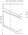
- an amount of silica gel powder is determined by an experiment of Fig.3.
- the experiment was carried out by changing an amount of silica gel powder and placing the panel at an elevated temperature and a high humidity to determine deterioration degree.
- the results are expressed as a graph in Fig.3.
- a shows a thin film EL panel without the moisture-absorption sheet or layer
- b shows one having a surface density of 0.1 g/m
- c is 1 g/m
- d is 10 g/m
- e is 500 g/m.
- a line expressed as f in Fig.3 is a limit over which a quality of a thin film EL panel is bad.
- surface densities more than 10 g/m significantly lengthen a life span of the panel. It is very difficult from the technical view points to disperse silica gel powder in a surface density of more than 500 g/m. Technical effects do not increase in proportion to the increase of surface density. Accordingly, a surface density of silica gel powder is defined as within the range of 10 to 500 g/m.
- the moisture-absorption sheet 14 and layer 15 are colored black or near black.
- the EL element of dot-matrix type is explained, but the present invention may also be applied to an element of dot-matrix type.
- the present invention since the moisture-absorption sheet or layer is present between the moisture-proof sheet and the EL element, the thin film EL panel has a long life span.
- the present invention can realize to make light and thin in comparison with conventional techniques.
- the present invention has no process for pouring silicone oil and easily produces the thin film EL panel, it makes low cost.
- the moisture-absorption sheet or layer is colored black, it enhances the contrast of display.
Landscapes
- Electroluminescent Light Sources (AREA)
Claims (4)
- Panneau électroluminescent (EL) à film mince comportant une plaque de base perméable et légère (2), un élément EL à film mince (1) déposé sur la plaque de base (2) et recouvert d'une feuille d'encapsulation hermétique (12) qui est constituée d'une feuille externe de protection contre l'humidité (13) et d'une feuille interne d'absorption de l'humidité (14) tourné vers l'élément EL (1), un espace (16) étant ménagé entre la couche d'absorption de l'humidité (14) et l'élément EL (1), la feuille d'encapsulation hermétique (12) étant soudée au niveau de sa partie périphérique à la plaque de base (2), caractérisé en ce que la feuille d'absorption de l'humidité (14) comporte une feuille de polymère organique sur laquelle est dispersée de la poudre de gel de silice selon une densité surfacique de 10 à 500 g / m, et en ce que la feuille de protection contre l'humidité (13) comporte deux films organiques (22) entre lesquels s'intercale un film métallique (21).
- Panneau EL à film mince (1) selon la revendication 1, dans lequel ladite feuille d'absorption de l'humidité (14) a une épaisseur de 0,01 à 1 mm.
- Panneau électroluminescent (EL) à film mince comportant une plaque de base perméable et légère (2), un élément EL à film mince (1) déposé sur la plaque de base (2) et recouvert d'une feuille d'encapsulation hermétique (12) qui est constituée d'une feuille externe de protection contre l'humidité (13) et d'une couche interne d'absorption de l'humidité (15) tourné vers l'élément EL (1), un espace (16) étant ménagé entre la couche d'absorption de l'humidité (15) et l'élément EL (1), la feuille d'encapsulation hermétique (12) étant soudée au niveau de sa partie périphérique à la plaque de base (2), caractérisé en ce que la couche d'absorption de l'humidité (15) est constituée de poudre de gel de silice dispersée sur la surface de la feuille de protection contre l'humidité (13) selon une densité surfacique de 10 à 500 g / m, et en ce que la feuille de protection contre l'humidité (13) comporte deux films organiques (22) entre lesquels s'intercale un film métallique (21).
- Panneau EL à film mince (1) selon la revendication 1 ou la revendication 3, dans lequel ladite feuille d'absorption de l'humidité (14) ou ladite couche d'absorption de l'humidité (15) est colorée en noir ou en une teinte proche du noir.
Applications Claiming Priority (2)
| Application Number | Priority Date | Filing Date | Title |
|---|---|---|---|
| JP175569/88 | 1988-07-14 | ||
| JP63175569A JP2742057B2 (ja) | 1988-07-14 | 1988-07-14 | 薄膜elパネル |
Publications (3)
| Publication Number | Publication Date |
|---|---|
| EP0350907A2 EP0350907A2 (fr) | 1990-01-17 |
| EP0350907A3 EP0350907A3 (en) | 1990-03-14 |
| EP0350907B1 true EP0350907B1 (fr) | 1996-05-01 |
Family
ID=15998374
Family Applications (1)
| Application Number | Title | Priority Date | Filing Date |
|---|---|---|---|
| EP89112799A Expired - Lifetime EP0350907B1 (fr) | 1988-07-14 | 1989-07-13 | Panneau électroluminescent à film mince |
Country Status (5)
| Country | Link |
|---|---|
| US (1) | US5124204A (fr) |
| EP (1) | EP0350907B1 (fr) |
| JP (1) | JP2742057B2 (fr) |
| DE (1) | DE68926365T2 (fr) |
| FI (1) | FI98262C (fr) |
Cited By (7)
| Publication number | Priority date | Publication date | Assignee | Title |
|---|---|---|---|---|
| US7991677B2 (en) | 2004-10-29 | 2011-08-02 | American Express Travel Related Services Company, Inc. | Using commercial share of wallet to rate investments |
| US9058627B1 (en) | 2002-05-30 | 2015-06-16 | Consumerinfo.Com, Inc. | Circular rotational interface for display of consumer credit information |
| US9508092B1 (en) | 2007-01-31 | 2016-11-29 | Experian Information Solutions, Inc. | Systems and methods for providing a direct marketing campaign planning environment |
| US9558519B1 (en) | 2011-04-29 | 2017-01-31 | Consumerinfo.Com, Inc. | Exposing reporting cycle information |
| US9563916B1 (en) | 2006-10-05 | 2017-02-07 | Experian Information Solutions, Inc. | System and method for generating a finance attribute from tradeline data |
| US9569797B1 (en) | 2002-05-30 | 2017-02-14 | Consumerinfo.Com, Inc. | Systems and methods of presenting simulated credit score information |
| US11847693B1 (en) | 2014-02-14 | 2023-12-19 | Experian Information Solutions, Inc. | Automatic generation of code for attributes |
Families Citing this family (128)
| Publication number | Priority date | Publication date | Assignee | Title |
|---|---|---|---|---|
| JPH0329291A (ja) * | 1989-06-27 | 1991-02-07 | Sumitomo Bakelite Co Ltd | 有機分散型elランプ用捕水フィルム |
| DE69128524T2 (de) * | 1990-10-17 | 1998-04-16 | Mitsubishi Chem Corp | Hitze- und feuchtigkeitsbeständiger film |
| DE69129907T2 (de) * | 1990-11-30 | 1998-12-10 | Idemitsu Kosan Co. Ltd., Tokio/Tokyo | Organische elektroluminszente vorrichtung |
| JPH04267096A (ja) * | 1991-02-21 | 1992-09-22 | Sharp Corp | 薄膜elパネル |
| US5491377A (en) * | 1993-08-03 | 1996-02-13 | Janusauskas; Albert | Electroluminescent lamp and method |
| JP2795207B2 (ja) * | 1994-03-31 | 1998-09-10 | 株式会社デンソー | エレクトロルミネッセンス表示器及びその製造方法 |
| US5771562A (en) * | 1995-05-02 | 1998-06-30 | Motorola, Inc. | Passivation of organic devices |
| US5585695A (en) * | 1995-06-02 | 1996-12-17 | Adrian Kitai | Thin film electroluminescent display module |
| WO1997016053A1 (fr) * | 1995-10-20 | 1997-05-01 | Robert Bosch Gmbh | Systeme stratifie electroluminescent |
| JPH09148066A (ja) * | 1995-11-24 | 1997-06-06 | Pioneer Electron Corp | 有機el素子 |
| US5874804A (en) * | 1997-03-03 | 1999-02-23 | Motorola, Inc. | Organic electroluminescent device hermetic encapsulation package and method of fabrication |
| US5952778A (en) * | 1997-03-18 | 1999-09-14 | International Business Machines Corporation | Encapsulated organic light emitting device |
| JP3290375B2 (ja) * | 1997-05-12 | 2002-06-10 | 松下電器産業株式会社 | 有機電界発光素子 |
| US7126161B2 (en) | 1998-10-13 | 2006-10-24 | Semiconductor Energy Laboratory Co., Ltd. | Semiconductor device having El layer and sealing material |
| US6274887B1 (en) | 1998-11-02 | 2001-08-14 | Semiconductor Energy Laboratory Co., Ltd. | Semiconductor device and manufacturing method therefor |
| US7141821B1 (en) * | 1998-11-10 | 2006-11-28 | Semiconductor Energy Laboratory Co., Ltd. | Semiconductor device having an impurity gradient in the impurity regions and method of manufacture |
| US7022556B1 (en) | 1998-11-11 | 2006-04-04 | Semiconductor Energy Laboratory Co., Ltd. | Exposure device, exposure method and method of manufacturing semiconductor device |
| US6277679B1 (en) | 1998-11-25 | 2001-08-21 | Semiconductor Energy Laboratory Co., Ltd. | Method of manufacturing thin film transistor |
| EP1524708A3 (fr) | 1998-12-16 | 2006-07-26 | Battelle Memorial Institute | Matière de barrière contre les conditions d'ambiance et son procédé de fabrication |
| US6268695B1 (en) | 1998-12-16 | 2001-07-31 | Battelle Memorial Institute | Environmental barrier material for organic light emitting device and method of making |
| JP3817081B2 (ja) * | 1999-01-29 | 2006-08-30 | パイオニア株式会社 | 有機el素子の製造方法 |
| US7697052B1 (en) | 1999-02-17 | 2010-04-13 | Semiconductor Energy Laboratory Co., Ltd. | Electronic view finder utilizing an organic electroluminescence display |
| US6680487B1 (en) | 1999-05-14 | 2004-01-20 | Semiconductor Energy Laboratory Co., Ltd. | Semiconductor comprising a TFT provided on a substrate having an insulating surface and method of fabricating the same |
| TWI240592B (en) * | 1999-06-03 | 2005-09-21 | Koninkl Philips Electronics Nv | Organic electroluminescent device |
| US7288420B1 (en) | 1999-06-04 | 2007-10-30 | Semiconductor Energy Laboratory Co., Ltd. | Method for manufacturing an electro-optical device |
| TW527735B (en) | 1999-06-04 | 2003-04-11 | Semiconductor Energy Lab | Electro-optical device |
| US8853696B1 (en) | 1999-06-04 | 2014-10-07 | Semiconductor Energy Laboratory Co., Ltd. | Electro-optical device and electronic device |
| TW516244B (en) * | 1999-09-17 | 2003-01-01 | Semiconductor Energy Lab | EL display device and method for manufacturing the same |
| JP3942770B2 (ja) * | 1999-09-22 | 2007-07-11 | 株式会社半導体エネルギー研究所 | El表示装置及び電子装置 |
| US6876145B1 (en) | 1999-09-30 | 2005-04-05 | Semiconductor Energy Laboratory Co., Ltd. | Organic electroluminescent display device |
| TW480722B (en) * | 1999-10-12 | 2002-03-21 | Semiconductor Energy Lab | Manufacturing method of electro-optical device |
| US6623861B2 (en) * | 2001-04-16 | 2003-09-23 | Battelle Memorial Institute | Multilayer plastic substrates |
| IT1313899B1 (it) * | 1999-10-25 | 2002-09-26 | Getters Spa | Sistema assorbitore di umidita' per schermi comprendenti diodiorganici emettitori di luce e processo per la sua produzione |
| US6413645B1 (en) | 2000-04-20 | 2002-07-02 | Battelle Memorial Institute | Ultrabarrier substrates |
| US6866901B2 (en) * | 1999-10-25 | 2005-03-15 | Vitex Systems, Inc. | Method for edge sealing barrier films |
| US6573652B1 (en) | 1999-10-25 | 2003-06-03 | Battelle Memorial Institute | Encapsulated display devices |
| US7198832B2 (en) * | 1999-10-25 | 2007-04-03 | Vitex Systems, Inc. | Method for edge sealing barrier films |
| US6548912B1 (en) | 1999-10-25 | 2003-04-15 | Battelle Memorial Institute | Semicoductor passivation using barrier coatings |
| US20100330748A1 (en) | 1999-10-25 | 2010-12-30 | Xi Chu | Method of encapsulating an environmentally sensitive device |
| KR100720066B1 (ko) | 1999-11-09 | 2007-05-18 | 가부시키가이샤 한도오따이 에네루기 켄큐쇼 | 발광장치 제작방법 |
| US6646287B1 (en) | 1999-11-19 | 2003-11-11 | Semiconductor Energy Laboratory Co., Ltd. | Semiconductor device with tapered gate and insulating film |
| JP3409764B2 (ja) | 1999-12-28 | 2003-05-26 | 日本電気株式会社 | 有機el表示パネルの製造方法 |
| US20010053559A1 (en) * | 2000-01-25 | 2001-12-20 | Semiconductor Energy Laboratory Co., Ltd. | Method of fabricating display device |
| JP4526682B2 (ja) | 2000-03-28 | 2010-08-18 | 日東電工株式会社 | エレクトロルミネッセンス素子 |
| US6492026B1 (en) | 2000-04-20 | 2002-12-10 | Battelle Memorial Institute | Smoothing and barrier layers on high Tg substrates |
| US6605826B2 (en) | 2000-08-18 | 2003-08-12 | Semiconductor Energy Laboratory Co., Ltd. | Light-emitting device and display device |
| US6924594B2 (en) * | 2000-10-03 | 2005-08-02 | Semiconductor Energy Laboratory Co., Ltd. | Light emitting device |
| JP4094804B2 (ja) * | 2000-10-17 | 2008-06-04 | 三星エスディアイ株式会社 | 有機el装置の製造方法 |
| TW518910B (en) | 2000-12-20 | 2003-01-21 | Koninkl Philips Electronics Nv | Device, particularly an electroluminescent display device, and method of manufacturing such a device |
| US7222981B2 (en) * | 2001-02-15 | 2007-05-29 | Semiconductor Energy Laboratory Co., Ltd. | EL display device and electronic device |
| US6822391B2 (en) * | 2001-02-21 | 2004-11-23 | Semiconductor Energy Laboratory Co., Ltd. | Light emitting device, electronic equipment, and method of manufacturing thereof |
| CN100380703C (zh) * | 2001-05-18 | 2008-04-09 | 皇家菲利浦电子有限公司 | 吸湿板 |
| US7294517B2 (en) * | 2001-06-18 | 2007-11-13 | Semiconductor Energy Laboratory Co., Ltd. | Light emitting device and method of fabricating the same |
| US7211828B2 (en) * | 2001-06-20 | 2007-05-01 | Semiconductor Energy Laboratory Co., Ltd. | Light emitting device and electronic apparatus |
| TW548860B (en) | 2001-06-20 | 2003-08-21 | Semiconductor Energy Lab | Light emitting device and method of manufacturing the same |
| TW546857B (en) * | 2001-07-03 | 2003-08-11 | Semiconductor Energy Lab | Light-emitting device, method of manufacturing a light-emitting device, and electronic equipment |
| US8415208B2 (en) | 2001-07-16 | 2013-04-09 | Semiconductor Energy Laboratory Co., Ltd. | Semiconductor device and peeling off method and method of manufacturing semiconductor device |
| TW558743B (en) * | 2001-08-22 | 2003-10-21 | Semiconductor Energy Lab | Peeling method and method of manufacturing semiconductor device |
| ITMI20011895A1 (it) * | 2001-09-11 | 2003-03-11 | Saes Getters P A | Dispositivo assorbitore di umidita' per schermi comprendenti diodi organici emettitori di luce e processo per la sua produzione |
| US6470594B1 (en) * | 2001-09-21 | 2002-10-29 | Eastman Kodak Company | Highly moisture-sensitive electronic device element and method for fabrication utilizing vent holes or gaps |
| JP4166455B2 (ja) * | 2001-10-01 | 2008-10-15 | 株式会社半導体エネルギー研究所 | 偏光フィルム及び発光装置 |
| JP4019690B2 (ja) * | 2001-11-02 | 2007-12-12 | セイコーエプソン株式会社 | 電気光学装置及びその製造方法並びに電子機器 |
| ITMI20012524A1 (it) * | 2001-11-30 | 2003-05-30 | Getters Spa | Dispositivo assorbitore di umidita' di ridotto spessore e processo per la sua produzione |
| JP4010394B2 (ja) * | 2001-12-14 | 2007-11-21 | 大日本印刷株式会社 | エレクトロルミネッセント素子 |
| US8900366B2 (en) | 2002-04-15 | 2014-12-02 | Samsung Display Co., Ltd. | Apparatus for depositing a multilayer coating on discrete sheets |
| US8808457B2 (en) | 2002-04-15 | 2014-08-19 | Samsung Display Co., Ltd. | Apparatus for depositing a multilayer coating on discrete sheets |
| JP2003323973A (ja) * | 2002-04-26 | 2003-11-14 | Sanyo Electric Co Ltd | エレクトロルミネッセンス表示装置 |
| KR20030085911A (ko) * | 2002-05-02 | 2003-11-07 | 주식회사 엘리아테크 | 유기 전계 발광 표시소자 및 그의 제조방법 |
| EP1506693B1 (fr) * | 2002-05-10 | 2006-09-27 | Koninklijke Philips Electronics N.V. | Panneau electroluminescent |
| US20050175841A1 (en) * | 2002-05-10 | 2005-08-11 | Koninklijke Philips Electronics N.V. | Electroluminescent panel |
| US7164155B2 (en) * | 2002-05-15 | 2007-01-16 | Semiconductor Energy Laboratory Co., Ltd. | Light emitting device |
| US7230271B2 (en) | 2002-06-11 | 2007-06-12 | Semiconductor Energy Laboratory Co., Ltd. | Light emitting device comprising film having hygroscopic property and transparency and manufacturing method thereof |
| US7710019B2 (en) | 2002-12-11 | 2010-05-04 | Samsung Electronics Co., Ltd. | Organic light-emitting diode display comprising auxiliary electrodes |
| US6843578B1 (en) | 2002-12-17 | 2005-01-18 | James Cheung | Electro-luminescent footwear or clothing system |
| US7648925B2 (en) * | 2003-04-11 | 2010-01-19 | Vitex Systems, Inc. | Multilayer barrier stacks and methods of making multilayer barrier stacks |
| US7510913B2 (en) | 2003-04-11 | 2009-03-31 | Vitex Systems, Inc. | Method of making an encapsulated plasma sensitive device |
| KR100496286B1 (ko) * | 2003-04-12 | 2005-06-17 | 삼성에스디아이 주식회사 | 유기 전계 발광 표시 장치 및 이의 제조 방법 |
| KR100544127B1 (ko) * | 2003-08-27 | 2006-01-23 | 삼성에스디아이 주식회사 | 수분 흡수층을 구비한 유기 전계 발광 표시 장치 |
| KR100544128B1 (ko) * | 2003-08-28 | 2006-01-23 | 삼성에스디아이 주식회사 | 다공성 물질층을 구비한 유기 전계 발광 표시 장치 |
| US20050070196A1 (en) * | 2003-09-29 | 2005-03-31 | Colombo Frank J. | Protecting electro-optical devices with a fluoropolymer |
| US7049745B2 (en) * | 2003-11-25 | 2006-05-23 | Eastman Kodak Company | OLED display having thermally conductive layer |
| US7495644B2 (en) * | 2003-12-26 | 2009-02-24 | Semiconductor Energy Laboratory Co., Ltd. | Display device and method for manufacturing display device |
| RU2328836C1 (ru) * | 2004-02-26 | 2008-07-10 | Тосиба Матириалс Ко., Лтд. | Электролюминесцентное покрытие для подсветки переключателя, переключатель с подсветкой и электронное устройство с таким переключателем |
| US7202504B2 (en) | 2004-05-20 | 2007-04-10 | Semiconductor Energy Laboratory Co., Ltd. | Light-emitting element and display device |
| EP1617494B1 (fr) | 2004-07-02 | 2010-08-11 | Konarka Technologies, Inc. | Dispositif photovoltaïque organique avec encapsulation |
| US8732004B1 (en) | 2004-09-22 | 2014-05-20 | Experian Information Solutions, Inc. | Automated analysis of data to generate prospect notifications based on trigger events |
| US20060066234A1 (en) * | 2004-09-29 | 2006-03-30 | Chun-Chung Lu | Organic electro-luminescent display panel and method of fabricating the same |
| US7767498B2 (en) * | 2005-08-25 | 2010-08-03 | Vitex Systems, Inc. | Encapsulated devices and method of making |
| US7711636B2 (en) | 2006-03-10 | 2010-05-04 | Experian Information Solutions, Inc. | Systems and methods for analyzing data |
| TWI324493B (en) * | 2006-05-19 | 2010-05-01 | Au Optronics Corp | Lectro-luminescence panel, el panel |
| US8088502B2 (en) * | 2006-09-20 | 2012-01-03 | Battelle Memorial Institute | Nanostructured thin film optical coatings |
| DE202006015495U1 (de) * | 2006-10-09 | 2007-03-08 | Degussa Ag | Elektrolumineszent ausgestattete Artikel |
| US8606666B1 (en) | 2007-01-31 | 2013-12-10 | Experian Information Solutions, Inc. | System and method for providing an aggregation tool |
| JP5208591B2 (ja) * | 2007-06-28 | 2013-06-12 | 株式会社半導体エネルギー研究所 | 発光装置、及び照明装置 |
| US9690820B1 (en) | 2007-09-27 | 2017-06-27 | Experian Information Solutions, Inc. | Database system for triggering event notifications based on updates to database records |
| CN101453803B (zh) * | 2007-11-29 | 2011-07-06 | 比亚迪股份有限公司 | 一种电致发光片及其制作方法 |
| US8053984B2 (en) * | 2008-05-26 | 2011-11-08 | Lg Display Co., Ltd. | Organic light emitting diode display |
| JP2011003522A (ja) | 2008-10-16 | 2011-01-06 | Semiconductor Energy Lab Co Ltd | フレキシブル発光装置、電子機器及びフレキシブル発光装置の作製方法 |
| US9184410B2 (en) | 2008-12-22 | 2015-11-10 | Samsung Display Co., Ltd. | Encapsulated white OLEDs having enhanced optical output |
| US9337446B2 (en) | 2008-12-22 | 2016-05-10 | Samsung Display Co., Ltd. | Encapsulated RGB OLEDs having enhanced optical output |
| US8219408B2 (en) * | 2008-12-29 | 2012-07-10 | Motorola Mobility, Inc. | Audio signal decoder and method for producing a scaled reconstructed audio signal |
| US20100174638A1 (en) | 2009-01-06 | 2010-07-08 | ConsumerInfo.com | Report existence monitoring |
| US8766269B2 (en) | 2009-07-02 | 2014-07-01 | Semiconductor Energy Laboratory Co., Ltd. | Light-emitting device, lighting device, and electronic device |
| US8590338B2 (en) | 2009-12-31 | 2013-11-26 | Samsung Mobile Display Co., Ltd. | Evaporator with internal restriction |
| US9000442B2 (en) * | 2010-01-20 | 2015-04-07 | Semiconductor Energy Laboratory Co., Ltd. | Light-emitting device, flexible light-emitting device, electronic device, and method for manufacturing light-emitting device and flexible-light emitting device |
| TWI589042B (zh) * | 2010-01-20 | 2017-06-21 | 半導體能源研究所股份有限公司 | 發光裝置,撓性發光裝置,電子裝置,照明設備,以及發光裝置和撓性發光裝置的製造方法 |
| US9652802B1 (en) | 2010-03-24 | 2017-05-16 | Consumerinfo.Com, Inc. | Indirect monitoring and reporting of a user's credit data |
| TWI540939B (zh) | 2010-09-14 | 2016-07-01 | 半導體能源研究所股份有限公司 | 固態發光元件,發光裝置和照明裝置 |
| JP5827104B2 (ja) | 2010-11-19 | 2015-12-02 | 株式会社半導体エネルギー研究所 | 照明装置 |
| TWI591871B (zh) | 2010-12-16 | 2017-07-11 | 半導體能源研究所股份有限公司 | 發光裝置及照明裝置 |
| US8735874B2 (en) | 2011-02-14 | 2014-05-27 | Semiconductor Energy Laboratory Co., Ltd. | Light-emitting device, display device, and method for manufacturing the same |
| KR101922603B1 (ko) | 2011-03-04 | 2018-11-27 | 가부시키가이샤 한도오따이 에네루기 켄큐쇼 | 발광 장치, 조명 장치, 기판, 기판의 제작 방법 |
| KR102079188B1 (ko) | 2012-05-09 | 2020-02-19 | 가부시키가이샤 한도오따이 에네루기 켄큐쇼 | 발광 장치 및 전자 기기 |
| US10255598B1 (en) | 2012-12-06 | 2019-04-09 | Consumerinfo.Com, Inc. | Credit card account data extraction |
| KR102309244B1 (ko) | 2013-02-20 | 2021-10-05 | 가부시키가이샤 한도오따이 에네루기 켄큐쇼 | 반도체 장치 |
| US9870589B1 (en) | 2013-03-14 | 2018-01-16 | Consumerinfo.Com, Inc. | Credit utilization tracking and reporting |
| CN105793957B (zh) | 2013-12-12 | 2019-05-03 | 株式会社半导体能源研究所 | 剥离方法及剥离装置 |
| KR20150097359A (ko) | 2014-02-18 | 2015-08-26 | 주식회사 엘지화학 | 봉지 필름 및 이를 포함하는 유기전자장치 |
| US10242019B1 (en) | 2014-12-19 | 2019-03-26 | Experian Information Solutions, Inc. | User behavior segmentation using latent topic detection |
| US11410230B1 (en) | 2015-11-17 | 2022-08-09 | Consumerinfo.Com, Inc. | Realtime access and control of secure regulated data |
| US10757154B1 (en) | 2015-11-24 | 2020-08-25 | Experian Information Solutions, Inc. | Real-time event-based notification system |
| EP3555837B1 (fr) | 2017-01-31 | 2026-06-17 | Experian Information Solutions, Inc. | Ingestion de données hétérogènes à grande échelle et résolution d'utilisateur |
| CN107833978B (zh) * | 2017-10-31 | 2021-12-10 | 昆山国显光电有限公司 | 一种显示器件 |
| US10671749B2 (en) | 2018-09-05 | 2020-06-02 | Consumerinfo.Com, Inc. | Authenticated access and aggregation database platform |
| US11588137B2 (en) | 2019-06-05 | 2023-02-21 | Semiconductor Energy Laboratory Co., Ltd. | Functional panel, display device, input/output device, and data processing device |
| US11659758B2 (en) | 2019-07-05 | 2023-05-23 | Semiconductor Energy Laboratory Co., Ltd. | Display unit, display module, and electronic device |
| US11844236B2 (en) | 2019-07-12 | 2023-12-12 | Semiconductor Energy Laboratory Co., Ltd. | Functional panel, display device, input/output device, and data processing device |
| WO2021069999A1 (fr) | 2019-10-11 | 2021-04-15 | 株式会社半導体エネルギー研究所 | Panneau fonctionnel, dispositif d'affichage, dispositif d'entrée/sortie et dispositif de traitement d'informations |
Family Cites Families (14)
| Publication number | Priority date | Publication date | Assignee | Title |
|---|---|---|---|---|
| FR1381497A (fr) * | 1962-11-01 | 1964-12-14 | Thomson Houston Comp Francaise | Dispositif de commutation supraconducteur |
| US3182209A (en) * | 1962-11-01 | 1965-05-04 | Gen Electric | Superconducting switching device utilizing plural control superconductors |
| GB1501878A (en) * | 1975-09-09 | 1978-02-22 | Thorn Electrical Ind Ltd | Electroluminescent panel |
| JPS5272197A (en) * | 1976-04-05 | 1977-06-16 | Sharp Corp | Thin film el device |
| US4104555A (en) * | 1977-01-27 | 1978-08-01 | Atkins & Merrill, Inc. | High temperature encapsulated electroluminescent lamp |
| JPS5583196A (en) * | 1978-12-20 | 1980-06-23 | Nippon Telegraph & Telephone | Method of sealing thin film electroluminescent element |
| GB2049274B (en) * | 1979-03-16 | 1983-04-27 | Sharp Kk | Moisture absorptive arrangement for a glass sealed thinfilm electroluminescent display panel |
| CH643967A5 (de) * | 1979-05-29 | 1984-06-29 | Ibm | Supraleitfaehige schalt- und speichervorrichtung. |
| US4767674A (en) * | 1984-01-27 | 1988-08-30 | Dainichi-Nippon Cables, Ltd. | Metal cored board and method for manufacturing same |
| JPS60185394A (ja) * | 1984-03-01 | 1985-09-20 | アルプス電気株式会社 | 電場発光装置 |
| JPS639998Y2 (fr) * | 1984-12-28 | 1988-03-24 | ||
| JPS6357230A (ja) * | 1986-08-29 | 1988-03-11 | 大日本印刷株式会社 | Elパネル用外装材 |
| JPS63105495A (ja) * | 1986-10-22 | 1988-05-10 | アルプス電気株式会社 | 薄膜elパネル |
| US5070070A (en) * | 1988-03-09 | 1991-12-03 | E. I. Du Pont De Nemours And Company | High temperature superconducting memory storage device and cryotron |
-
1988
- 1988-07-14 JP JP63175569A patent/JP2742057B2/ja not_active Expired - Lifetime
-
1989
- 1989-07-13 DE DE68926365T patent/DE68926365T2/de not_active Expired - Lifetime
- 1989-07-13 FI FI893396A patent/FI98262C/fi active IP Right Grant
- 1989-07-13 EP EP89112799A patent/EP0350907B1/fr not_active Expired - Lifetime
-
1991
- 1991-03-29 US US07/678,175 patent/US5124204A/en not_active Expired - Lifetime
Cited By (7)
| Publication number | Priority date | Publication date | Assignee | Title |
|---|---|---|---|---|
| US9058627B1 (en) | 2002-05-30 | 2015-06-16 | Consumerinfo.Com, Inc. | Circular rotational interface for display of consumer credit information |
| US9569797B1 (en) | 2002-05-30 | 2017-02-14 | Consumerinfo.Com, Inc. | Systems and methods of presenting simulated credit score information |
| US7991677B2 (en) | 2004-10-29 | 2011-08-02 | American Express Travel Related Services Company, Inc. | Using commercial share of wallet to rate investments |
| US9563916B1 (en) | 2006-10-05 | 2017-02-07 | Experian Information Solutions, Inc. | System and method for generating a finance attribute from tradeline data |
| US9508092B1 (en) | 2007-01-31 | 2016-11-29 | Experian Information Solutions, Inc. | Systems and methods for providing a direct marketing campaign planning environment |
| US9558519B1 (en) | 2011-04-29 | 2017-01-31 | Consumerinfo.Com, Inc. | Exposing reporting cycle information |
| US11847693B1 (en) | 2014-02-14 | 2023-12-19 | Experian Information Solutions, Inc. | Automatic generation of code for attributes |
Also Published As
| Publication number | Publication date |
|---|---|
| EP0350907A2 (fr) | 1990-01-17 |
| DE68926365D1 (de) | 1996-06-05 |
| JP2742057B2 (ja) | 1998-04-22 |
| FI98262C (fi) | 1997-05-12 |
| US5124204A (en) | 1992-06-23 |
| FI893396A0 (fi) | 1989-07-13 |
| DE68926365T2 (de) | 1996-11-28 |
| FI98262B (fi) | 1997-01-31 |
| EP0350907A3 (en) | 1990-03-14 |
| FI893396A7 (fi) | 1990-01-15 |
| JPH0224992A (ja) | 1990-01-26 |
Similar Documents
| Publication | Publication Date | Title |
|---|---|---|
| US5124204A (en) | Thin film electroluminescent (EL) panel | |
| US5189405A (en) | Thin film electroluminescent panel | |
| US4669632A (en) | Evacuated heat insulation unit | |
| US8663773B2 (en) | Vacuum insulation panel and method for manufacturing the same | |
| US5216536A (en) | Encapsulated electrochromic device and method for making same | |
| US8670173B2 (en) | SPD films and light valve laminates with improved durability | |
| US4357557A (en) | Glass sealed thin-film electroluminescent display panel free of moisture and the fabrication method thereof | |
| US3508810A (en) | Photochromic systems | |
| JPH05502487A (ja) | 高性能断熱多重枠ガラス構造 | |
| KR20010006343A (ko) | 방습 필름 및 전기장 발광 소자 | |
| FI105882B (fi) | Kosteudenpitävä sähköluminenssi-ohutkalvopaneeli | |
| US4425030A (en) | Liquid crystal display comprising an encapsulation and a liquid crystal display cell with poly-para-xylene and a method of manufacturing the same | |
| KR960031368A (ko) | 다층유리 | |
| US4315668A (en) | Permeation barrier for display cells | |
| JP2911693B2 (ja) | 真空断熱構造体 | |
| CN110828704A (zh) | 显示面板的封装方法及封装结构 | |
| US5885672A (en) | Coated barrier film and packaging utilizing the same and method | |
| JP2816582B2 (ja) | 熱線吸収板 | |
| JPS60250946A (ja) | 太陽電池モジュール用裏面保護シート | |
| JPH02197071A (ja) | 薄膜elパネル | |
| GB2077995A (en) | Panels incorporating photo-cells and method of manufacturing same | |
| JPH03246883A (ja) | 薄膜elパネル | |
| WO2006079713A1 (fr) | Support deshydratant comportant un indicateur de saturation d'humidite | |
| JPS63252391A (ja) | Elパネル | |
| JPH0793188B2 (ja) | 薄膜elパネル |
Legal Events
| Date | Code | Title | Description |
|---|---|---|---|
| PUAI | Public reference made under article 153(3) epc to a published international application that has entered the european phase |
Free format text: ORIGINAL CODE: 0009012 |
|
| AK | Designated contracting states |
Kind code of ref document: A2 Designated state(s): DE FR GB |
|
| PUAL | Search report despatched |
Free format text: ORIGINAL CODE: 0009013 |
|
| AK | Designated contracting states |
Kind code of ref document: A3 Designated state(s): DE FR GB |
|
| 17P | Request for examination filed |
Effective date: 19900706 |
|
| 17Q | First examination report despatched |
Effective date: 19920929 |
|
| GRAH | Despatch of communication of intention to grant a patent |
Free format text: ORIGINAL CODE: EPIDOS IGRA |
|
| GRAA | (expected) grant |
Free format text: ORIGINAL CODE: 0009210 |
|
| AK | Designated contracting states |
Kind code of ref document: B1 Designated state(s): DE FR GB |
|
| REF | Corresponds to: |
Ref document number: 68926365 Country of ref document: DE Date of ref document: 19960605 |
|
| ET | Fr: translation filed | ||
| PLBE | No opposition filed within time limit |
Free format text: ORIGINAL CODE: 0009261 |
|
| STAA | Information on the status of an ep patent application or granted ep patent |
Free format text: STATUS: NO OPPOSITION FILED WITHIN TIME LIMIT |
|
| 26N | No opposition filed | ||
| REG | Reference to a national code |
Ref country code: GB Ref legal event code: IF02 |
|
| PGFP | Annual fee paid to national office [announced via postgrant information from national office to epo] |
Ref country code: DE Payment date: 20080717 Year of fee payment: 20 |
|
| PGFP | Annual fee paid to national office [announced via postgrant information from national office to epo] |
Ref country code: FR Payment date: 20080718 Year of fee payment: 20 |
|
| PGFP | Annual fee paid to national office [announced via postgrant information from national office to epo] |
Ref country code: GB Payment date: 20080716 Year of fee payment: 20 |
|
| REG | Reference to a national code |
Ref country code: GB Ref legal event code: PE20 Expiry date: 20090712 |
|
| PG25 | Lapsed in a contracting state [announced via postgrant information from national office to epo] |
Ref country code: GB Free format text: LAPSE BECAUSE OF EXPIRATION OF PROTECTION Effective date: 20090712 |