EP0350911A2 - Structure multiprocesseur à couplage rigide pour une application en temps réel - Google Patents
Structure multiprocesseur à couplage rigide pour une application en temps réel Download PDFInfo
- Publication number
- EP0350911A2 EP0350911A2 EP89112824A EP89112824A EP0350911A2 EP 0350911 A2 EP0350911 A2 EP 0350911A2 EP 89112824 A EP89112824 A EP 89112824A EP 89112824 A EP89112824 A EP 89112824A EP 0350911 A2 EP0350911 A2 EP 0350911A2
- Authority
- EP
- European Patent Office
- Prior art keywords
- memory
- bus
- interrupt
- processor
- multiprocessor
- Prior art date
- Legal status (The legal status is an assumption and is not a legal conclusion. Google has not performed a legal analysis and makes no representation as to the accuracy of the status listed.)
- Withdrawn
Links
Images


Classifications
-
- G—PHYSICS
- G06—COMPUTING OR CALCULATING; COUNTING
- G06F—ELECTRIC DIGITAL DATA PROCESSING
- G06F15/00—Digital computers in general; Data processing equipment in general
- G06F15/76—Architectures of general purpose stored program computers
- G06F15/80—Architectures of general purpose stored program computers comprising an array of processing units with common control, e.g. single instruction multiple data processors
- G06F15/8007—Architectures of general purpose stored program computers comprising an array of processing units with common control, e.g. single instruction multiple data processors single instruction multiple data [SIMD] multiprocessors
- G06F15/8015—One dimensional arrays, e.g. rings, linear arrays, buses
Definitions
- This invention relates generally to multiprocessor systems applied in real-time systems. More specifically, it relates to a tightly coupled multiprocessor structure in which multiple processors operate simultaneously in order to balance three key performance attributes: speed of CPU computation, high I/O throughput and an efficient interrupt handling capability.
- Existing structures of multiple processors are typically designed to improve the performance of the Central Processing Unit (CPU). These structures apply pipelining, which divides computation into a number of steps, or parallalism, which uses multiple resources.
- Existing multi processor structures can be categorized into: (a) loosely coupled, and (b) tightly coupled.
- the loosely coupled multiprocessors consist of independent processors connected via high speed communication links. They have separate copies of operating systems.
- all CPUs share global memory, and there is a single copy of the operating system and data structures. There is no synchronization problem, however, global memory bus represents a system bottle-neck.
- Existing tightly coupled multiprocessor structures improve the speed of computation, however, the computation power of a computer cannot be accomplished solely by high performance of the CPU, especially in the area of real-time computing and intensive I/O operations.
- this object is met by providing a multiprocessor system which comprises a number of N processor units, M input-output devices, a common Global Memory, a memory bus and means to operate a plurality of different peripherial devices, wherein a system support processor, and an a event bus are provided and wherein said system support processor performs interrupt handling of data streams and said event bus performs interrupt distribution among the elements of the multi processor system.
- memory bus contention problem is solved by a Memory Bus which connects the common memory to all CPUs and I/O modules and which consists of four independent, 32-bit buses with a high clock rate.
- the local memory in all CPUs provides the storage of critical operating system instructions, non-user interrupt service routines and private non-shared data.
- a high speed semaphore processor built in hardware significantly reduces semaphore based global memory bus transactions.
- An event bus allows the multiprocessor system to handle a large number of interrupts by load balancing of real-time interrupts. Event bus control is provided by a central event control, while modules are interfaced to the event bus via an interrupt controller.
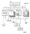
- Fig. 1 an overall embodiment of the invention is shown.
- the system consists of a number of CPU units (2 to 20) 1, a number of I/O units (2 to 10) 2, a Storage Server (SS) 3 and a System Support Processor (SSP) 4. They all share global memory via the Memory Bus 5. There is a single copy of the operating system placed in the global memory 6. Interrupt handling is performed by a Central Event Control unit placed in the SSP 4, while the interrupt distribution is done via the Event Bus (EB) 7.
- EB Event Bus
- the memory Bus (MB) 5 consists of four independent 32-bit buses with a 12.5 MHz clock rate.
- the MB is a synchronous bus with non-multiplexed address and data bits. This allows a data transfer rate of 50 Mbytes/sec.
- Each of the four buses operates concurrently with a maximum aggregate bandwidth of 200 Mbytes/sec.
- the MB has three types of bus cycles:
- the arbitration function required to handle bus sharing on the MB is performed by a Central Arbitration Unit (CAU).
- CAU Central Arbitration Unit
- the arbitration cycles are pipelined with access cycles, as shown in Fig. 2.
- the arbitration signals consist of one request and one grant from each agent on the bus.
- the arbitration algorithm is based on two rotating queues with a fixed priority between queues.
- the Event Bus is a synchronous multifunction bus.
- the data bus portion of the bus provides a vehicle on which interrupts, priority resolution, and interrupt tagging information is passed.
- the control portion of the bus defines at any given time the mode that the Event Bus is operating in.
- the Event Bus is the vehicle in which the interrupt requesting agents and interrupt servicing agent resolve all source and destination routing.
- the Event Bus consists of 32 data lines, 4 interrupt identification lines, 3 interrupt cycle function lines and a synchronization clock.
- the data lines are multiplexed to provide 16 levels of prioritized interrupts and 16 interrupt enable lines.
- the codes of the Event Bus are defined as an interrupt processing method used to process a specific interrupt. There are six modes of operation: 1) distributed priority interrupts, 2) task activation interrupts, 3) message based interrupts, 4) global common interrupts, 5) non-maskable interrupt and 6) local interrupts.
- the Distributed Priority Interrupt mode allows interrupts to be processed by the most available servicing agent that is enabled to handle that level.
- the Task Activation Interrupt mode allows an interrupt to be processed by the most available sevicing agent that is able to change to the new task level, which implies any servicing agent that is currently running lower than the new task level.
- the Message Based Interrupt mode allows a requesting agent to send an interrupt to a specific servicing agent.
- the Global Common Interrupt mode is a method by which a requesting agent may broadcast an interrupt to all servicing agents that are enabled to handle that interrupt level.
- the Non-Maskable Interrupt mode is an interrupt that cannot be ignored. This mode is used to warn all modules in the system that power is going away.
- the Local Interrupts are not part of the Event Bus global interrupt scheme. These interrupts are used to connect local events to the prioritized interrupt structure.
- the Event Bus 7 allows the system to handle a large number of interrupts in a deterministic manner.
- Event Bus timing and control are provided by Central Interrupt Control Unit (CICU) placed in the SSP.
- the CICU also distributes interrupts in the multi-processor system via the Event Bus.
- the EB provides sixteen levels of hardware prioritized interrupts and has the ability to direct interrupts to the processor which is most able to handle the interrupt. This interrupt handling capability is based upon a programable value by each processor in the system. The programmable value directly relates to the task priority that is currently executing on each processor.
- the CPU units are interfaced to the Event Bus via Local Interrupt Control Units (LICU).
- the LICU contains all necessary logic to handle the Event Bus, plus the processor interface and the local interrupt structure.
- the Event Bus 7 is composed of three different types of functional interface elements as shown in Fig. 3. These elements are: requesting agents 8, servicing agents 9 and a central interrupt control 10. The requesting and servicing agent functions both reside in the LICU.
- the CICU serves as a common control element that prioritizes interrupts and generates the Event Bus Control and timing signals.
- the LICU provides the interface between a processor module and the Event Bus.
- the primary logic blocks of the LICU are the requesting agent block 8, the servicing agent block 9 and the logical interrupt interface 10.
- the requesting agent block has all the necessary logic to generate all levels of interrupts, with the exception of a non-maskable interrupt.
- This logic includes the Event Bus requesting logic, the Event Bus acknowledge logic, the interrupt identification and source tag logic, and the necessary logic to support all of the interrupt categories.
- the servicing agent block contains all necessary logic to handle interrupts.
- This logic includes the interrupt requesting, enabled and active registers, the interrupt vector registers, interrupt configuration, and the active interrupt level control logic.
- Local interrupts interface contains the elements needed to interface the LICU to a processor module.
- This logic includes the NMI (non-masking interrupt) and the INTR (Interrupt) request signals, the address and data interface, interrupt acknowledge logic and the miscel
- Each CPU 1 unit consists of: (a) a high-performance 32-bit single chip CPU, which typically has on-chip bus interface unit, instruction decode and execution units, and memory management unit, (b) floating point coprocessor, (c) local memory, (d) cache controller and cache memory, (e) local interrupt controller unit, (f) memory bus controller and (g) semaphore assist logic.
- Local memory is used for storing Operating Sytem (OS) instructions, non-user interrupt service routines, and private non-shared data for fast access. Local access of the OS instructions and data increases bus bandwidth to other bus agents by avoiding access of the Memory Bus.
- OS Operating Sytem
- non-user interrupt service routines non-user interrupt service routines
- private non-shared data for fast access.
- Local access of the OS instructions and data increases bus bandwidth to other bus agents by avoiding access of the Memory Bus.
- the cache memory improves the performance of the global memory (DRAM) by providing the CPU with a small amount of high speed SRAM.
- the cache contains a copy of frequently accessed global memory locations, thus providing the performance of a large SRAM based global memory.
- Each cache consists of 64 Kbytes of high speed SRAM based cache data buffer.
- the cache is controlled by a Cache Controller, which intercepts the CPU memory agents and checks if the SRAM has the data requested by the CPU. If the SRAM does not, the Cache Controller performs the global memory access and stores the received data in the SRAM as well as passing it to the CPU.
- the Cache controller is made up of four cache tag circuits, one per 32-bit bus 5. Each cache tag circuit interfaces to its region of the cache data buffer.
- the cache system features include: (a) Cache coherency maintained by bus watching, (b) Tag RAM and compare circuitry, (c) Write through cache data buffer, and (d) Direct mapped with bus associative properties.
- Each CPU contains four Memory Bus Controllers.
- Each controller contains data and address FIFOs and logic to arbitrate and control access to and from the bus.
- the System Support Processor consists of a CPU unit, RAM and EPROM memory, Memory Bus and Event Bus interfaces, operator interfaces, Small Computer System Interface (SCSI) and a Semaphore Processor. Only the Semaphore Processor is illustrated in Fig. 1 in detail.
- the Semaphore Processor is an extension of the CPU/Memory environment.
- the Semaphore Processor incorporates software semaphore algorithms in a hardware state machine that is connected to the Memory Bus via the controllers.
- the Semaphore Processor consists of a hardware sequencer, 1 Mbyte RAM, and the MB interface.
- Software semaphore algorithms are encoded in memory read addressed that are intercepted and serviced by the SP. Within the addresses received, two fields are used to specify the particular type of the algorithm and the semaphore memory address to be operated upon. In this approach, the SP appears to the other components of the system as a memory agent.
- the MB memory protocol is adhered to by SP, minimizing the effort to invoke a semaphore operation. Bus locking is not required due to the SP operating upon the semaphore data on a first-come, first-serve basis.
- the Global Memory 6 is a high capacity, high speed, DRAM memory which serves the agents using simple memory operations.
- the Storage Server 3 is intended to serve as a high performance interface to all disc and tape peripherals. Designed around an ultra high speed microprocessor, the Storage Server 3 supports a large disc cache system, performs virtual memory transaction, and a variety of embedded utility functions.
- the SS provides a modular interface to the SCSI (Small Computer System Interface) peripheral devices.
- the memory system reduces the contention in the following ways: (a) up to 16-way interleaving address scheme, (b) memory agents have highest level of MB arbitration priority, (c) copy of non-data structure portion of the operating system resides in each CPU's local memory, (d) copy of OS interrupt routines reside in each CPU's local memory, (e) system semaphore operations are routed to a separate semaphore processor with its own semaphore memory.
- the interleaving global memory addressing scheme is intended to balance accesses equally among all memory subsystems. By increasing the number of memory subsystems, and thus the interleave factor, contention for any one array is reduced.
- a memory subsystem has the ability to perform multiple word accesses consisting of double, triple or quad words. The memory subsystem decodes the access type information from the source/access tag it receives during a request-to-read operation.
- the global memory addressing scheme allows sequential access by non-memory devices to be evently distributed over the four independent buses.
- Each memory board 11 has four separate address, data and control buses, each with a bandwidth of 50 Mbytes/second for a total of 200 Mbytes/second.
- Each memory board contains four 32-bit arrays 12 (A to D) and supports the byte enable scheme.
- the byte enable signals are used to decode which of the bytes are being accessed, two address bits are used to indicate which array is selected, while the other two address bits are used to indicate which board is being selected.
- This decode scheme makes the memory subsystem appear as a 128-bit memory block.
- the four independent buses reduce contention for the global memory significantly.
Landscapes
- Engineering & Computer Science (AREA)
- Computer Hardware Design (AREA)
- Theoretical Computer Science (AREA)
- Computing Systems (AREA)
- Physics & Mathematics (AREA)
- General Engineering & Computer Science (AREA)
- General Physics & Mathematics (AREA)
- Multi Processors (AREA)
Applications Claiming Priority (2)
| Application Number | Priority Date | Filing Date | Title |
|---|---|---|---|
| US22043088A | 1988-07-13 | 1988-07-13 | |
| US220430 | 1988-07-13 |
Publications (2)
| Publication Number | Publication Date |
|---|---|
| EP0350911A2 true EP0350911A2 (fr) | 1990-01-17 |
| EP0350911A3 EP0350911A3 (fr) | 1990-09-05 |
Family
ID=22823515
Family Applications (1)
| Application Number | Title | Priority Date | Filing Date |
|---|---|---|---|
| EP19890112824 Withdrawn EP0350911A3 (fr) | 1988-07-13 | 1989-07-13 | Structure multiprocesseur à couplage rigide pour une application en temps réel |
Country Status (1)
| Country | Link |
|---|---|
| EP (1) | EP0350911A3 (fr) |
Cited By (3)
| Publication number | Priority date | Publication date | Assignee | Title |
|---|---|---|---|---|
| EP0530310A4 (en) * | 1990-05-18 | 1993-07-21 | Star Semiconductor Corporation | Programmable signal processor architecture |
| DE4326740C1 (de) * | 1993-08-09 | 1994-10-13 | Martin Kopp | Architektur für eine Rechenanlage |
| WO1996029656A1 (fr) * | 1995-03-21 | 1996-09-26 | Newbridge Networks Corporation | Systeme de communications interprocesseur |
-
1989
- 1989-07-13 EP EP19890112824 patent/EP0350911A3/fr not_active Withdrawn
Non-Patent Citations (2)
| Title |
|---|
| ELECTRO AND MINI/MICRO NORTHEAST, 23rd - 25th April 1985, pages 1-23, New York, US; S. PRI-TAL et al.: "VMEsystem: The most popular 32-bit architecture" * |
| IEEE MICRO, vol. 5, no. 1, February 1985, pages 53-66, IEEE, New York, US; H. KIRRMANN: "Events and interrupts in tightly coupled multiprocessors" * |
Cited By (4)
| Publication number | Priority date | Publication date | Assignee | Title |
|---|---|---|---|---|
| EP0530310A4 (en) * | 1990-05-18 | 1993-07-21 | Star Semiconductor Corporation | Programmable signal processor architecture |
| DE4326740C1 (de) * | 1993-08-09 | 1994-10-13 | Martin Kopp | Architektur für eine Rechenanlage |
| US5842013A (en) * | 1993-08-09 | 1998-11-24 | Kopp; Martin | Architecture for modular computer system in which one of the modules is dedicated to user-interface task |
| WO1996029656A1 (fr) * | 1995-03-21 | 1996-09-26 | Newbridge Networks Corporation | Systeme de communications interprocesseur |
Also Published As
| Publication number | Publication date |
|---|---|
| EP0350911A3 (fr) | 1990-09-05 |
Similar Documents
| Publication | Publication Date | Title |
|---|---|---|
| US20240184446A1 (en) | Multi-processor bridge with cache allocate awareness | |
| EP0886225B1 (fr) | Architecture de microprocesseurs pouvant prendre en charge plusieurs processeurs hétérogènes | |
| US5446910A (en) | Interrupt controller with automatic distribution of interrupts for a multiple processor computer system | |
| US5388237A (en) | Method of and apparatus for interleaving multiple-channel DMA operations | |
| US5706514A (en) | Distributed execution of mode mismatched commands in multiprocessor computer systems | |
| US5386532A (en) | Method and apparatus for transferring data between a memory and a plurality of peripheral units through a plurality of data channels | |
| EP0348654A2 (fr) | Méthode et appareil pour augmenter le débit d'un système | |
| EP0523764A2 (fr) | Système d'ordinateur muni d'une interconnection directe parbus entre le processeur et la mémoire principale dynamique et d'une commande DMA incorporée au processeur, pour une pluralité de moyens d'échange de données égalament raccordés audit bus, et processeur central destiné à être utilisé dans un tel système d'ordinateur | |
| EP0426184A2 (fr) | Protocole de commande pour un interface de type bus maître | |
| JP2004506981A (ja) | マルチプロセッサにおけるセマフォおよびアトミック動作の管理のためのシステムおよび方法 | |
| US20040019728A1 (en) | Multiple hardware partitions under one input/output hub | |
| US5778236A (en) | Multiprocessing interrupt controller on I/O bus | |
| US5765195A (en) | Method for distributing interprocessor interrupt requests via cache memory coherency mechanisms | |
| US6789168B2 (en) | Embedded DRAM cache | |
| US5524211A (en) | System for employing select, pause, and identification registers to control communication among plural processors | |
| US5668975A (en) | Method of requesting data by interlacing critical and non-critical data words of multiple data requests and apparatus therefor | |
| US20030229721A1 (en) | Address virtualization of a multi-partitionable machine | |
| US5953535A (en) | Using intelligent bus bridges with pico-code to service interrupts and improve interrupt response | |
| US5894578A (en) | System and method for using random access memory in a programmable interrupt controller | |
| US5517671A (en) | System for designating a plurality of I/O devices to a plurality of I/O channels and connecting and buffering the plurality of I/O channels to a single system bus | |
| US6647450B1 (en) | Multiprocessor computer systems with command FIFO buffer at each target device | |
| JPS63253448A (ja) | マルチ計算機装置 | |
| Männer et al. | The Heidelberg POLYP—A flexible and fault-tolerant poly-processor | |
| JPS63310060A (ja) | マルチプロセツサシステム | |
| Aude et al. | The MULTIPLUS/MULPLIX parallel processing environment |
Legal Events
| Date | Code | Title | Description |
|---|---|---|---|
| PUAI | Public reference made under article 153(3) epc to a published international application that has entered the european phase |
Free format text: ORIGINAL CODE: 0009012 |
|
| AK | Designated contracting states |
Kind code of ref document: A2 Designated state(s): DE FR GB |
|
| PUAL | Search report despatched |
Free format text: ORIGINAL CODE: 0009013 |
|
| AK | Designated contracting states |
Kind code of ref document: A3 Designated state(s): DE FR GB |
|
| 17P | Request for examination filed |
Effective date: 19901206 |
|
| STAA | Information on the status of an ep patent application or granted ep patent |
Free format text: STATUS: THE APPLICATION IS DEEMED TO BE WITHDRAWN |
|
| 18D | Application deemed to be withdrawn |
Effective date: 19930202 |