EP0350939A1 - Méthode et dispositif de branchement pour la compensation des écarts de tension dans un circuit pour la mise au point et/ou le suivi de piste - Google Patents
Méthode et dispositif de branchement pour la compensation des écarts de tension dans un circuit pour la mise au point et/ou le suivi de piste Download PDFInfo
- Publication number
- EP0350939A1 EP0350939A1 EP89112884A EP89112884A EP0350939A1 EP 0350939 A1 EP0350939 A1 EP 0350939A1 EP 89112884 A EP89112884 A EP 89112884A EP 89112884 A EP89112884 A EP 89112884A EP 0350939 A1 EP0350939 A1 EP 0350939A1
- Authority
- EP
- European Patent Office
- Prior art keywords
- output
- input
- focus
- photodiodes
- control loop
- Prior art date
- Legal status (The legal status is an assumption and is not a legal conclusion. Google has not performed a legal analysis and makes no representation as to the accuracy of the status listed.)
- Granted
Links
- 238000000034 method Methods 0.000 title claims abstract description 52
- 238000005286 illumination Methods 0.000 claims description 5
- 230000000717 retained effect Effects 0.000 claims description 4
- 101150087426 Gnal gene Proteins 0.000 claims 1
- 238000013500 data storage Methods 0.000 abstract 1
- 230000003287 optical effect Effects 0.000 description 22
- 239000008186 active pharmaceutical agent Substances 0.000 description 7
- 230000032683 aging Effects 0.000 description 4
- 230000007774 longterm Effects 0.000 description 1
Images


Classifications
-
- G—PHYSICS
- G11—INFORMATION STORAGE
- G11B—INFORMATION STORAGE BASED ON RELATIVE MOVEMENT BETWEEN RECORD CARRIER AND TRANSDUCER
- G11B7/00—Recording or reproducing by optical means, e.g. recording using a thermal beam of optical radiation by modifying optical properties or the physical structure, reproducing using an optical beam at lower power by sensing optical properties; Record carriers therefor
- G11B7/08—Disposition or mounting of heads or light sources relatively to record carriers
- G11B7/09—Disposition or mounting of heads or light sources relatively to record carriers with provision for moving the light beam or focus plane for the purpose of maintaining alignment of the light beam relative to the record carrier during transducing operation, e.g. to compensate for surface irregularities of the latter or for track following
-
- G—PHYSICS
- G11—INFORMATION STORAGE
- G11B—INFORMATION STORAGE BASED ON RELATIVE MOVEMENT BETWEEN RECORD CARRIER AND TRANSDUCER
- G11B21/00—Head arrangements not specific to the method of recording or reproducing
- G11B21/02—Driving or moving of heads
- G11B21/10—Track finding or aligning by moving the head ; Provisions for maintaining alignment of the head relative to the track during transducing operation, i.e. track following
- G11B21/106—Track finding or aligning by moving the head ; Provisions for maintaining alignment of the head relative to the track during transducing operation, i.e. track following on disks
-
- G—PHYSICS
- G11—INFORMATION STORAGE
- G11B—INFORMATION STORAGE BASED ON RELATIVE MOVEMENT BETWEEN RECORD CARRIER AND TRANSDUCER
- G11B7/00—Recording or reproducing by optical means, e.g. recording using a thermal beam of optical radiation by modifying optical properties or the physical structure, reproducing using an optical beam at lower power by sensing optical properties; Record carriers therefor
- G11B7/08—Disposition or mounting of heads or light sources relatively to record carriers
- G11B7/09—Disposition or mounting of heads or light sources relatively to record carriers with provision for moving the light beam or focus plane for the purpose of maintaining alignment of the light beam relative to the record carrier during transducing operation, e.g. to compensate for surface irregularities of the latter or for track following
- G11B7/0901—Disposition or mounting of heads or light sources relatively to record carriers with provision for moving the light beam or focus plane for the purpose of maintaining alignment of the light beam relative to the record carrier during transducing operation, e.g. to compensate for surface irregularities of the latter or for track following for track following only
- G11B7/0903—Multi-beam tracking systems
-
- G—PHYSICS
- G11—INFORMATION STORAGE
- G11B—INFORMATION STORAGE BASED ON RELATIVE MOVEMENT BETWEEN RECORD CARRIER AND TRANSDUCER
- G11B7/00—Recording or reproducing by optical means, e.g. recording using a thermal beam of optical radiation by modifying optical properties or the physical structure, reproducing using an optical beam at lower power by sensing optical properties; Record carriers therefor
- G11B7/08—Disposition or mounting of heads or light sources relatively to record carriers
- G11B7/09—Disposition or mounting of heads or light sources relatively to record carriers with provision for moving the light beam or focus plane for the purpose of maintaining alignment of the light beam relative to the record carrier during transducing operation, e.g. to compensate for surface irregularities of the latter or for track following
- G11B7/0908—Disposition or mounting of heads or light sources relatively to record carriers with provision for moving the light beam or focus plane for the purpose of maintaining alignment of the light beam relative to the record carrier during transducing operation, e.g. to compensate for surface irregularities of the latter or for track following for focusing only
- G11B7/0909—Disposition or mounting of heads or light sources relatively to record carriers with provision for moving the light beam or focus plane for the purpose of maintaining alignment of the light beam relative to the record carrier during transducing operation, e.g. to compensate for surface irregularities of the latter or for track following for focusing only by astigmatic methods
-
- G—PHYSICS
- G11—INFORMATION STORAGE
- G11B—INFORMATION STORAGE BASED ON RELATIVE MOVEMENT BETWEEN RECORD CARRIER AND TRANSDUCER
- G11B7/00—Recording or reproducing by optical means, e.g. recording using a thermal beam of optical radiation by modifying optical properties or the physical structure, reproducing using an optical beam at lower power by sensing optical properties; Record carriers therefor
- G11B7/08—Disposition or mounting of heads or light sources relatively to record carriers
- G11B7/09—Disposition or mounting of heads or light sources relatively to record carriers with provision for moving the light beam or focus plane for the purpose of maintaining alignment of the light beam relative to the record carrier during transducing operation, e.g. to compensate for surface irregularities of the latter or for track following
- G11B7/094—Methods and circuits for servo offset compensation
-
- G—PHYSICS
- G11—INFORMATION STORAGE
- G11B—INFORMATION STORAGE BASED ON RELATIVE MOVEMENT BETWEEN RECORD CARRIER AND TRANSDUCER
- G11B7/00—Recording or reproducing by optical means, e.g. recording using a thermal beam of optical radiation by modifying optical properties or the physical structure, reproducing using an optical beam at lower power by sensing optical properties; Record carriers therefor
- G11B7/08—Disposition or mounting of heads or light sources relatively to record carriers
- G11B7/09—Disposition or mounting of heads or light sources relatively to record carriers with provision for moving the light beam or focus plane for the purpose of maintaining alignment of the light beam relative to the record carrier during transducing operation, e.g. to compensate for surface irregularities of the latter or for track following
- G11B7/0945—Methods for initialising servos, start-up sequences
Definitions
- the invention relates to a method for compensating offset voltages in a focus control loop, by means of which a light beam from a light source is focused on a record carrier, and / or in a track control loop, by means of which the light beam is guided on the data tracks of the record carrier, the light beam from Recording medium is reflected on a photodetector with a plurality of photodiodes, from whose output voltages the focus error and / or tracking error signal is generated by forming the difference.
- a light beam is focused on the record carrier by means of a focus control loop and guided on the data tracks of the record carrier by means of a track control loop.
- the optical scanning device of such devices as, for example, CD players, magneto-optical devices for playback and recording, recording and playback devices of DRAW discs or video disc players is equipped with a laser diode, a plurality of lenses, a prism beam splitter, a diffraction grating and a photodetector. Structure and function of an optical pick-up, a so-called optical pick-up, are in electronic components & applications, Vol. 6, No. 4, 1984 on pages 209-215.
- the light beam emitted by the laser diode is focused onto the CD disk by means of lenses and from there is reflected onto a photodetector.
- the data stored on the CD disk and the actual value for the focus and the tracking control loop are obtained from the output signal of the photodetector.
- the actual value for the focus control loop is referred to as focusing error, while the expression radial tracking error is selected for the actual value of the track control loop.
- a coil serves as the actuator for the focus control loop, via the magnetic field of which an objective lens can be moved along the optical axis.
- the focus control loop now ensures that the light beam emitted by the laser diode is always focused on the CD disk.
- the track control loop which is often also referred to as a radial drive, the optical scanning device can be displaced in the radial direction with respect to the CD disk. This allows the light beam to be guided on the spiral data tracks on the CD.
- the radial drive is made up of a so-called coarse and a so-called fine drive.
- the coarse drive is designed, for example, as a spindle, by means of which the entire optical scanning device comprising the laser diode, the lenses, the prism beam splitter, the diffraction grating and the photodetector can be moved radially.
- the fine drive the light beam can be tilted in the radial direction, for example, by a predeterminable small angle, so that the light beam can travel a small distance along a radius of the CD disk solely by this tilting movement.
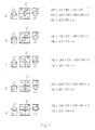
- FIG. 1 shows the photodetector PD of the optical scanning device of a CD player, in which three laser beams L1, L2 and L3 are focused on the CD disk.
- Such a scanning device is called three-beam pick-up in the literature mentioned at the beginning.
- the middle light beam L1 is the main beam
- the two light beams L2 and L3 are the beams +1. and -1.
- photodetector PD In the photodetector PD, four square-shaped photodiodes A, B, C and D are assembled so that they in turn form a square. With regard to this square formed from the four photodiodes A, B, C and D, two further square-shaped photodiodes E and F are located diagonally opposite one another.
- the two outer light beams L2 and L3, of which the front L2 strikes the photodiode E and the rear L3 strikes the photodiode F, generate the tracking error signal TE ES-FS.
- AS, BS, CS, DS, ES and FS denote the photo voltages of the photodiodes A, B, C, D, E and F.
- the central light beam L1 is circular when it is focused precisely on the large square formed by the photodiodes A, B, C and D, while at Defocusing takes elliptical shape.
- FIG. 1b shows the one case of defocusing, that the objective lens is too far away from the CD disk.
- the focus control loop recognizes from the positive value of the focus error signal FE that the objective lens is too close to the CD disk. The objective lens is therefore moved away from the CD disk by the actuator until the focus error signal FE becomes zero.
- the tracking error signal TE has the value zero.
- FIG. 1b shows the case in which the light beams L1, L2 and L3 are shifted to the right of the track.
- the actuator of the tracking control loop now moves the optical scanning device to the left until the tracking error signal TE becomes zero.
- control amplifier of the focus control circuit also has an offset voltage, the size of which depends on the one hand on the temperature and on the other hand is subject to a long-term drift.
- the drift of the offset voltage and other parameters of an amplifier over time are caused by the aging of the amplifier.
- the focus error signal FE (AS + BS) - (BS + DS) is formed in a differential amplifier. Because this differential amplifier also has an offset voltage, and because the photodiodes A, B, C and D emit different voltages or currents at the same luminance in contrast to ideal photodiodes, there is another source of disturbing offset voltages.
- the invention solves this problem by comparing the focus error and / or tracking error signal with a predefinable reference variable when the control loop is closed, and by supplying a compensation variable to the actuator of the focus and / or tracking control loop, which is changed until the focus error and / or tracking error signal matches the reference variable.
- a second solution to this problem provides that in a first process step with an open or switched-off control loop and uniform illumination of the photodiodes to the focus error and / or tracking error signal, a first compensation variable is added and changed until the sum agrees with a first reference variable that then, in a second method step with a closed control loop, the focus error and / or tracking error signal is compared with a second reference variable and that the actuator of the focus and / or tracking control loop is supplied with a second compensation variable and is changed until the focus and / or tracking error signal matches the reference size.
- a third solution to this problem is that in a first process step with the control circuit open or switched off and with uniform illumination of the photodiodes, the focus and / or tracking error signal is stored as a reference variable, that in a second subsequent process step with the control circuit closed, the control circuit actuator Compensation variable supplied and changed until the focus and / or tracking error signal matches the stored reference quantity.
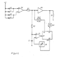
- FIG. 1 there is a voltage + U at the interconnected cathodes of the photodiodes A, B, C and D.
- the interconnected anodes of photodiodes A and C are connected to the addition input
- the interconnected anodes of photodiodes B and D are connected to the subtraction input of a differential amplifier DV, the output of which is connected via a resistor R1 to the input of a control amplifier RV and via a further resistor R2 is connected to the non-inverting input of a comparator VL.
- the non-inverting input of the comparator VL is at a reference potential via a capacitance C1.
- a reference voltage UR is present at the inverting input of the comparator VL, the output of which is connected to the input E1 of a microprocessor MP.
- the output A1 of the microprocessor MP is connected to the input of a digital-to-analog converter DA1, the output of which is connected to the output of the control amplifier RV and the one connection of the actuator SG is.
- the other connection of the actuator SG which is designed as a coil, is at reference potential.
- the focus control loop is constructed from ideal components which are not subject to any offset voltages.
- the main beam L1 forms a circle on the four photodiodes A, B, C and D, as shown in FIG. 1a. Because all four photodiodes A, B, C and D therefore receive the same light energy and convert it into an electrical current, they emit the same output voltages or currents. Therefore, the voltage at the output of the differential amplifier DV is zero. Because the control amplifier RV is also assumed to be ideal, the voltage at its output and therefore also at one connection of the actuator SG is also zero. The actuator SG, often also called the actuator, therefore moves the objective of the optical scanning device until the voltage at the output of the control amplifier RV becomes zero. Provided that ideal components are used, then the focus is precise because the voltage at the output of the differential amplifier DV is also zero.
- control amplifier RV has an offset voltage
- differential amplifier DV and the photodiodes A, B, C and D are still to be considered ideal.
- the actuator SG will move the lens until the voltage at the output of the control amplifier RV becomes zero.
- the control amplifier RV which is now assumed to be real, the input voltage and thus also the voltage at the output of the differential amplifier are then different from zero.
- the light beam L1 is therefore no longer circular, but how shown in Figure 1b or 1c slightly elliptical, indicating that is not precisely focused.
- the voltage at the output of the differential amplifier DV is compared in the comparator VL with a reference voltage UR, which is chosen to be zero in the exemplary embodiment specified.
- the microprocessor MP now changes the digital values at its output A1, which the digital-to-analog converter DA1 converts into an analog voltage and feeds the actuator SG until the comparator VL at the input E1 of the microprocessor MP indicates that the voltage at Output of the differential amplifier DV has become zero. Because the light beam L1 is now imaged circularly by the lens onto the photodiodes A, B, C and D, the focus is precise.
- the microprocessor MP maintains the value at its output A1, so that an analogue is constantly being used because of the digital-to-analog converter DA1 Compensation voltage is present at actuator SG.
- the device e.g. a CD player is now ready to play. It is particularly advantageous to carry out the compensation each time the CD player is switched on.
- the offset voltage of the control amplifier RV changes, for example as a result of aging or temperature fluctuations, this has the consequence that the voltage at the output of the differential amplifier DV also changes and no longer corresponds to the reference voltage UR. Because the comparator VL indicates this to the microprocessor MP when the CD player is switched on, the microprocessor is able to readjust the offset compensation voltage and thus to ensure optimal compensation.
- a major advantage of the circuit arrangement shown in FIG. 2 is that the offset voltage of the control amplifier RV is automatically compensated each time the CD player is switched on.
- the circuit arrangement from FIG. 3 differs from the circuit arrangement from FIG. 2 in that it is supplemented by a digital-to-analog converter DA2, the output of which is connected to the output of the differential amplifier DV and the input of which is connected to an output A2 of the microprocessor MP.
- DA2 digital-to-analog converter
- the differential amplifier DV also has an offset voltage.
- the photodiodes A, B, C and D are also real, i.e. not considered completely identical components that emit different voltages or currents with the same lighting. Therefore, in the case of focusing, if the lens images the light beam L1 in a circular manner as in FIG Value, e.g. accept + a.
- the four photodiodes A, B, C and D are evenly illuminated when the focus control loop is open or switched off. This state can be easily achieved by switching off the light source, because then the photodiodes A, B, C and D are in the dark. When the light source is switched off, it also does not matter where the lens is located and whether it is moving because no feedback can take place.
- the digital values which the microprocessor MP now outputs at its output A2 are converted into an analog voltage by the digital / analog converter DA2.
- the microprocessor MP now changes the digital values at its output A2 until the comparator VL indicates that the analog voltage at the output of the digital-to-analog converter DA2 has compensated for the voltage at the output of the differential amplifier DV.
- the digital value at this time at the output A2 of the microprocessor MP is retained. This measure ensures that the voltage at the input of the control amplifier RV is zero when the light beam L1 is imaged circularly onto the photodiodes A, B, C and D as in FIG.
- optical offset another previously neglected offset size, often referred to as optical offset, is due to the optics of the optical pickup. This means the following: If the light beam is precisely focused on the recording medium, the light beam does not become, as is the case with ideal, completely error-free optical components, due to the never-to-be-avoided optical errors of the optical components - the lenses, the prism beam splitter and the diffraction grating would be circular, but slightly elliptical on the photodetector with the four photodiodes A, B, C and D. If the light beam is precisely focused on the recording medium, the voltage at the output of the differential amplifier DV is therefore not zero, as desired, despite compensation for its offset voltage. Rather, it has a positive or negative value.
- an output A3 of the microprocessor MP is connected to the control input of the reference voltage source UR, which e.g. can be designed as a digital-to-analog converter.
- a fixed value is selected for the reference voltage UR.
- a third process step to compensate for the optical offset mentioned is carried out during the production of the CD player, which proceeds as follows.
- a CD test plate is inserted into the CD player.
- the digital values determined in the first and second method step at the outputs A1 and A2 of the microprocessor MP are retained during the third method step and are not changed.
- the light beam is now focused precisely on the recording medium, the CD test plate.
- the exact focusing is determined with the help of the CD test plate, because with precise focusing the jitter in the RF signal is the lowest. However, the exact focusing can also be checked, for example, using a microscope. It is now determined by what value the reference voltage UR is to be changed, so that the optical offset is also compensated, because the offset voltage of the differential amplifier DV was compensated in the first and that of the control amplifier RV in the second step.
- the reference voltage UR is therefore changed until the jitter in the HF signal assumes a minimum because the light beam is then focused precisely on the inserted test plate. The one on this The value of the reference voltage UR found in this way is fixed. The CD player is now ready for use.
- the offset voltage of the differential amplifier DV or the control amplifier RV changes in later game operation, they will e.g. compensated each time the device is switched on in accordance with the first and second process steps.
- the photodiodes A, B, C and D are uniformly illuminated by switching off the light source.
- the microprocessor MP changes the reference voltage UR until the comparator VL1 indicates to it that the reference voltage UR with the voltage at the output of the differential amplifier DV, which, for example + a may be the same.
- the first method step is changed in a manner similar to that in the circuit arrangement from FIG. 3.
- the focus control loop open or switched off, the light beam is precisely focused on the CD disk during production of the CD player and the exact focusing is checked with the aid of a microscope or by determining the jitter minimum in the HF signal using the CD test plate.
- the microprocessor MP changes the reference voltage UR until the comparator VL1 indicates that the ref limit voltage UR corresponds to the voltage at the output of the differential amplifier DV, which may be + b, for example.
- the second method step takes place with the light source switched on.
- the actuator SG would hold the lens in a position in which the voltage at the output of the control amplifier RV becomes zero.
- the voltage at the input of the control amplifier RV will generally not be + a or + b as desired, as would be the case with precise focusing, but rather a positive or negative value different from zero depending on the size of the offset voltage of the control amplifier RV.
- the microprocessor MP changes the digital value at its output A1, which is converted by the digital-to-analog converter DA1 into an analog compensation voltage supplied to the actuator SG, until the comparator VL indicates to it that the voltage at the output of the differential amplifier DV corresponds to the reference voltage UR, which has the value + a or + b in the assumed numerical example.
- the digital value then located at the output A1 of the microprocessor MP is retained, so that the correct analog compensation voltage is constantly applied to the actuator SG because of the digital-analog converter DA1.
- the CD player is now ready to play.
Landscapes
- Optical Recording Or Reproduction (AREA)
- Amplifiers (AREA)
- Networks Using Active Elements (AREA)
Priority Applications (1)
| Application Number | Priority Date | Filing Date | Title |
|---|---|---|---|
| AT89112884T ATE80960T1 (de) | 1988-07-15 | 1989-07-13 | Verfahren und schaltungsanordnung zur kompensation von offset-spannungen in einem fokus- und/oder spurregelkreis. |
Applications Claiming Priority (2)
| Application Number | Priority Date | Filing Date | Title |
|---|---|---|---|
| DE3824039 | 1988-07-15 | ||
| DE3824039A DE3824039A1 (de) | 1988-07-15 | 1988-07-15 | Verfahren und schaltungsanordnung zur kompensation von offset-spannungen in einem fokus- und/oder spurregelkreis |
Publications (2)
| Publication Number | Publication Date |
|---|---|
| EP0350939A1 true EP0350939A1 (fr) | 1990-01-17 |
| EP0350939B1 EP0350939B1 (fr) | 1992-09-23 |
Family
ID=6358758
Family Applications (2)
| Application Number | Title | Priority Date | Filing Date |
|---|---|---|---|
| EP89907726A Pending EP0378650A1 (fr) | 1988-07-15 | 1989-07-13 | Procede et systeme de montage pour compenser les tensions offset dans un circuit de reglage de focalisation et/ou de piste |
| EP89112884A Expired - Lifetime EP0350939B1 (fr) | 1988-07-15 | 1989-07-13 | Méthode et dispositif de branchement pour la compensation des écarts de tension dans un circuit pour la mise au point et/ou le suivi de piste |
Family Applications Before (1)
| Application Number | Title | Priority Date | Filing Date |
|---|---|---|---|
| EP89907726A Pending EP0378650A1 (fr) | 1988-07-15 | 1989-07-13 | Procede et systeme de montage pour compenser les tensions offset dans un circuit de reglage de focalisation et/ou de piste |
Country Status (14)
| Country | Link |
|---|---|
| US (1) | US5148423A (fr) |
| EP (2) | EP0378650A1 (fr) |
| JP (1) | JP2726131B2 (fr) |
| KR (1) | KR0145299B1 (fr) |
| CN (1) | CN1020007C (fr) |
| AT (1) | ATE80960T1 (fr) |
| DE (2) | DE3824039A1 (fr) |
| DK (1) | DK67990A (fr) |
| ES (1) | ES2035459T3 (fr) |
| GR (1) | GR3006012T3 (fr) |
| HK (1) | HK8997A (fr) |
| HU (1) | HUT53467A (fr) |
| MY (1) | MY104135A (fr) |
| WO (1) | WO1990000797A1 (fr) |
Cited By (2)
| Publication number | Priority date | Publication date | Assignee | Title |
|---|---|---|---|---|
| EP0450655A1 (fr) * | 1990-04-05 | 1991-10-09 | Sony Corporation | Appareil pour enregistrer des informations sur un disque optique et/ou reproduire de informations à partir d'un disque optique |
| US5415288A (en) * | 1990-02-08 | 1995-05-16 | Sony Corporation | Video cassette case having hard plastic sheets on flat surfaces thereof |
Families Citing this family (17)
| Publication number | Priority date | Publication date | Assignee | Title |
|---|---|---|---|---|
| JP2638279B2 (ja) * | 1990-09-28 | 1997-08-06 | ティアツク株式会社 | 光ディスク装置 |
| DE4102857A1 (de) * | 1991-01-31 | 1992-08-06 | Thomson Brandt Gmbh | Verfahren zum fokussieren eines lichtstrahls |
| JPH05159327A (ja) * | 1991-12-05 | 1993-06-25 | Hitachi Ltd | 光学式ディスクプレーヤにおけるフォーカスサーチ回路 |
| US5627818A (en) * | 1992-10-13 | 1997-05-06 | International Business Machines Corporation | Optical disk with marks used for calibrating an optical detector to minimize noise from undesired perturbations in disk surfaces |
| DE4323067A1 (de) * | 1993-07-10 | 1995-01-12 | Thomson Brandt Gmbh | G-Faktor-Abgleich |
| US5367513A (en) * | 1993-11-05 | 1994-11-22 | International Business Machines Corporation | Focus and tracking servo decoupling system |
| DE4415508A1 (de) * | 1994-05-03 | 1995-11-09 | Thomson Brandt Gmbh | Abtastgerät mit Adaptation |
| US5528577A (en) * | 1994-10-19 | 1996-06-18 | Sony Corporation | Apparatus and method for reading at least partially unmetallized optical discs |
| US20040213115A1 (en) * | 2001-05-11 | 2004-10-28 | Hideki Nakata | Optical head, disc recording/reproducing apparatus, and objective lens drive method |
| WO2003088229A1 (fr) * | 2002-04-17 | 2003-10-23 | Koninklijke Philips Electronics N.V. | Capteur optique |
| CN1331135C (zh) * | 2002-09-17 | 2007-08-08 | 联发科技股份有限公司 | 功率补偿电路与方法及具有该功率补偿电路的光学装置 |
| KR100529309B1 (ko) * | 2002-10-07 | 2005-11-17 | 삼성전자주식회사 | Dvd 플레이어의 오프셋 조정 장치 및 방법 |
| JP4152257B2 (ja) * | 2003-05-26 | 2008-09-17 | 三洋電機株式会社 | 光ディスク用オフセット調整回路、集積回路、光ディスク装置、及びオフセット調整方法 |
| US7313057B2 (en) * | 2003-07-18 | 2007-12-25 | Via Technologies, Inc. | Method for adjusting a control parameter and optical disc drive server system using the same |
| JP2005116079A (ja) * | 2003-10-08 | 2005-04-28 | Matsushita Electric Ind Co Ltd | ランドプリピットアドレス復調装置 |
| JP2007026486A (ja) * | 2005-07-12 | 2007-02-01 | Toshiba Corp | 受光素子回路及び光ディスク装置 |
| WO2016146725A1 (fr) * | 2015-03-17 | 2016-09-22 | Basf Se | Lecteur de données optiques |
Citations (2)
| Publication number | Priority date | Publication date | Assignee | Title |
|---|---|---|---|---|
| EP0088441A1 (fr) * | 1982-03-10 | 1983-09-14 | Hitachi, Ltd. | Système d'asservissement de focalisation verticale pour un lecteur de disque optique |
| EP0290882A1 (fr) * | 1987-05-09 | 1988-11-17 | Deutsche Thomson-Brandt GmbH | Appareil pour la reproduction de données |
Family Cites Families (5)
| Publication number | Priority date | Publication date | Assignee | Title |
|---|---|---|---|---|
| JPS58215736A (ja) * | 1982-06-07 | 1983-12-15 | Pioneer Electronic Corp | 光学式記録情報読取装置におけるサ−ボ装置 |
| JPS61177646A (ja) * | 1985-02-04 | 1986-08-09 | インタ−ナショナル ビジネス マシ−ンズ コ−ポレ−ション | 光学デイスク装置 |
| CA1261467A (fr) * | 1985-11-28 | 1989-09-26 | Akira Minami | Dispositif de commande de servomecanisme de focalisation pour lecteur de disques optiques a reglage du decalage |
| JPS63142533A (ja) * | 1986-12-03 | 1988-06-14 | Fujitsu Ltd | 光学的記録再生装置 |
| DE3732941A1 (de) * | 1987-09-30 | 1989-04-20 | Thomson Brandt Gmbh | Geraet zur wiedergabe von daten |
-
1988
- 1988-07-15 DE DE3824039A patent/DE3824039A1/de not_active Withdrawn
-
1989
- 1989-07-13 ES ES198989112884T patent/ES2035459T3/es not_active Expired - Lifetime
- 1989-07-13 DE DE8989112884T patent/DE58902327D1/de not_active Expired - Lifetime
- 1989-07-13 EP EP89907726A patent/EP0378650A1/fr active Pending
- 1989-07-13 WO PCT/EP1989/000816 patent/WO1990000797A1/fr not_active Ceased
- 1989-07-13 EP EP89112884A patent/EP0350939B1/fr not_active Expired - Lifetime
- 1989-07-13 HU HU894721A patent/HUT53467A/hu unknown
- 1989-07-13 AT AT89112884T patent/ATE80960T1/de not_active IP Right Cessation
- 1989-07-13 JP JP1507484A patent/JP2726131B2/ja not_active Expired - Lifetime
- 1989-07-13 KR KR1019900700555A patent/KR0145299B1/ko not_active Expired - Fee Related
- 1989-07-15 CN CN89104824A patent/CN1020007C/zh not_active Expired - Lifetime
- 1989-07-15 MY MYPI89000996A patent/MY104135A/en unknown
-
1990
- 1990-03-15 DK DK067990A patent/DK67990A/da not_active Application Discontinuation
-
1991
- 1991-09-30 US US07/769,331 patent/US5148423A/en not_active Expired - Lifetime
-
1992
- 1992-10-16 GR GR920402337T patent/GR3006012T3/el unknown
-
1997
- 1997-01-23 HK HK8997A patent/HK8997A/xx not_active IP Right Cessation
Patent Citations (2)
| Publication number | Priority date | Publication date | Assignee | Title |
|---|---|---|---|---|
| EP0088441A1 (fr) * | 1982-03-10 | 1983-09-14 | Hitachi, Ltd. | Système d'asservissement de focalisation verticale pour un lecteur de disque optique |
| EP0290882A1 (fr) * | 1987-05-09 | 1988-11-17 | Deutsche Thomson-Brandt GmbH | Appareil pour la reproduction de données |
Cited By (2)
| Publication number | Priority date | Publication date | Assignee | Title |
|---|---|---|---|---|
| US5415288A (en) * | 1990-02-08 | 1995-05-16 | Sony Corporation | Video cassette case having hard plastic sheets on flat surfaces thereof |
| EP0450655A1 (fr) * | 1990-04-05 | 1991-10-09 | Sony Corporation | Appareil pour enregistrer des informations sur un disque optique et/ou reproduire de informations à partir d'un disque optique |
Also Published As
| Publication number | Publication date |
|---|---|
| DE58902327D1 (de) | 1992-10-29 |
| ATE80960T1 (de) | 1992-10-15 |
| JP2726131B2 (ja) | 1998-03-11 |
| GR3006012T3 (fr) | 1993-06-21 |
| HUT53467A (en) | 1990-10-28 |
| DE3824039A1 (de) | 1990-01-18 |
| ES2035459T3 (es) | 1993-04-16 |
| DK67990A (da) | 1990-05-15 |
| HU894721D0 (en) | 1990-06-28 |
| EP0350939B1 (fr) | 1992-09-23 |
| JPH03502979A (ja) | 1991-07-04 |
| MY104135A (en) | 1994-02-28 |
| KR0145299B1 (ko) | 1998-07-01 |
| KR900702517A (ko) | 1990-12-07 |
| CN1020007C (zh) | 1993-03-03 |
| WO1990000797A1 (fr) | 1990-01-25 |
| DK67990D0 (da) | 1990-03-15 |
| EP0378650A1 (fr) | 1990-07-25 |
| HK8997A (en) | 1997-01-31 |
| US5148423A (en) | 1992-09-15 |
| CN1039919A (zh) | 1990-02-21 |
Similar Documents
| Publication | Publication Date | Title |
|---|---|---|
| EP0350939B1 (fr) | Méthode et dispositif de branchement pour la compensation des écarts de tension dans un circuit pour la mise au point et/ou le suivi de piste | |
| DE69624763T2 (de) | Verfahren und Gerät zum Abtasten einer mehrschichtigen Platte | |
| DE68916518T2 (de) | Optische Abtastvorrichtung mit einem Fokussierregelsystem sowie einer integrierten Schaltung zur Anwendung im Fokussierregelsystem. | |
| DE69431638T2 (de) | Automatische Fokusausgleicheinstellvorrichtung und Verfahren | |
| EP0313741B1 (fr) | Appareil pour reproduire des données | |
| EP0708961B1 (fr) | Egalisation du facteur g | |
| EP0320509B1 (fr) | Appareil de reproduction de donnees | |
| EP0309704B1 (fr) | Appareil pour la reproduction de données | |
| EP0290882B1 (fr) | Appareil pour la reproduction de données | |
| DE3704718A1 (de) | Geraet zur wiedergabe von daten | |
| EP0274031B1 (fr) | Circuit de régulation de suivi de piste pour positionner un faisceau de lumière | |
| EP0309719B1 (fr) | Appareil pour reproduire des données | |
| EP0399225A1 (fr) | Méthode de saut de piste | |
| EP0309705B1 (fr) | Méthode et appareil pour la compensation de la tension off-set d'un amplificateur de régulation | |
| DE3723923A1 (de) | Geraet zur wiedergabe von daten | |
| DE3743884C2 (de) | Optischer Datenprozessor | |
| EP0214194B1 (fr) | Procede et conception de circuit pour la focalisation d'un faisceau lumineux sur un support d'enregistrement optique | |
| DE4017485A1 (de) | Verfahren zur kompensation des offsets eines photodetektors | |
| DE4102857A1 (de) | Verfahren zum fokussieren eines lichtstrahls | |
| DE4103854A1 (de) | Optische abtastvorrichtung | |
| DE3901574A1 (de) | Optische abtastvorrichtung |
Legal Events
| Date | Code | Title | Description |
|---|---|---|---|
| PUAI | Public reference made under article 153(3) epc to a published international application that has entered the european phase |
Free format text: ORIGINAL CODE: 0009012 |
|
| AK | Designated contracting states |
Kind code of ref document: A1 Designated state(s): ES GR |
|
| 17P | Request for examination filed |
Effective date: 19900201 |
|
| RBV | Designated contracting states (corrected) |
Designated state(s): AT BE CH DE ES FR GB GR IT LI LU NL SE |
|
| XX | Miscellaneous (additional remarks) |
Free format text: VERBUNDEN MIT 89907726.7/0378650 (EUROPAEISCHE ANMELDENUMMER/VEROEFFENTLICHUNGSNUMMER) DURCH ENTSCHEIDUNG VOM 16.04.91. |
|
| 17Q | First examination report despatched |
Effective date: 19910430 |
|
| GRAA | (expected) grant |
Free format text: ORIGINAL CODE: 0009210 |
|
| AK | Designated contracting states |
Kind code of ref document: B1 Designated state(s): AT BE CH DE ES FR GB GR IT LI LU NL SE |
|
| PG25 | Lapsed in a contracting state [announced via postgrant information from national office to epo] |
Ref country code: IT Free format text: LAPSE BECAUSE OF FAILURE TO SUBMIT A TRANSLATION OF THE DESCRIPTION OR TO PAY THE FEE WITHIN THE PRE;WARNING: LAPSES OF ITALIAN PATENTS WITH EFFECTIVE DATE BEFORE 2007 MAY HAVE OCCURRED AT ANY TIME BEFORE 2007. THE CORRECT EFFECTIVE DATE MAY BE DIFFERENT FROM THE ONE RECORDED.SCRIBED TIME-LIMIT Effective date: 19920923 Ref country code: GR Free format text: LAPSE BECAUSE OF FAILURE TO SUBMIT A TRANSLATION OF THE DESCRIPTION OR TO PAY THE FEE WITHIN THE PRESCRIBED TIME-LIMIT Effective date: 19920923 |
|
| REF | Corresponds to: |
Ref document number: 80960 Country of ref document: AT Date of ref document: 19921015 Kind code of ref document: T |
|
| XX | Miscellaneous (additional remarks) |
Free format text: VERBUNDEN MIT 89907726.7/0378650 (EUROPAEISCHE ANMELDENUMMER/VEROEFFENTLICHUNGSNUMMER) DURCH ENTSCHEIDUNG VOM 16.04.91. |
|
| GBT | Gb: translation of ep patent filed (gb section 77(6)(a)/1977) | ||
| REF | Corresponds to: |
Ref document number: 58902327 Country of ref document: DE Date of ref document: 19921029 |
|
| ET | Fr: translation filed | ||
| REG | Reference to a national code |
Ref country code: ES Ref legal event code: FG2A Ref document number: 2035459 Country of ref document: ES Kind code of ref document: T3 |
|
| REG | Reference to a national code |
Ref country code: GR Ref legal event code: FG4A Free format text: 3006012 |
|
| PG25 | Lapsed in a contracting state [announced via postgrant information from national office to epo] |
Ref country code: AT Effective date: 19930713 |
|
| PG25 | Lapsed in a contracting state [announced via postgrant information from national office to epo] |
Ref country code: SE Effective date: 19930714 |
|
| PLBE | No opposition filed within time limit |
Free format text: ORIGINAL CODE: 0009261 |
|
| STAA | Information on the status of an ep patent application or granted ep patent |
Free format text: STATUS: NO OPPOSITION FILED WITHIN TIME LIMIT |
|
| PG25 | Lapsed in a contracting state [announced via postgrant information from national office to epo] |
Ref country code: BE Effective date: 19930731 Ref country code: CH Effective date: 19930731 Ref country code: LI Effective date: 19930731 Ref country code: LU Free format text: LAPSE BECAUSE OF NON-PAYMENT OF DUE FEES Effective date: 19930731 |
|
| 26N | No opposition filed | ||
| BERE | Be: lapsed |
Owner name: DEUTSCHE THOMSON-BRANDT G.M.B.H. Effective date: 19930731 |
|
| PG25 | Lapsed in a contracting state [announced via postgrant information from national office to epo] |
Ref country code: NL Effective date: 19940201 |
|
| NLV4 | Nl: lapsed or anulled due to non-payment of the annual fee | ||
| REG | Reference to a national code |
Ref country code: CH Ref legal event code: PL |
|
| REG | Reference to a national code |
Ref country code: GR Ref legal event code: MM2A Free format text: 3006012 |
|
| EUG | Se: european patent has lapsed |
Ref document number: 89112884.5 Effective date: 19940210 |
|
| REG | Reference to a national code |
Ref country code: GB Ref legal event code: 746 Effective date: 19970904 |
|
| REG | Reference to a national code |
Ref country code: FR Ref legal event code: D6 |
|
| REG | Reference to a national code |
Ref country code: GB Ref legal event code: IF02 |
|
| PGFP | Annual fee paid to national office [announced via postgrant information from national office to epo] |
Ref country code: ES Payment date: 20080821 Year of fee payment: 20 Ref country code: DE Payment date: 20080711 Year of fee payment: 20 |
|
| PGFP | Annual fee paid to national office [announced via postgrant information from national office to epo] |
Ref country code: FR Payment date: 20080721 Year of fee payment: 20 |
|
| PGFP | Annual fee paid to national office [announced via postgrant information from national office to epo] |
Ref country code: GB Payment date: 20080630 Year of fee payment: 20 |
|
| REG | Reference to a national code |
Ref country code: FR Ref legal event code: ST Effective date: 20090331 |
|
| REG | Reference to a national code |
Ref country code: GB Ref legal event code: PE20 Expiry date: 20090712 |
|
| REG | Reference to a national code |
Ref country code: ES Ref legal event code: FD2A Effective date: 20090714 |
|
| PG25 | Lapsed in a contracting state [announced via postgrant information from national office to epo] |
Ref country code: ES Free format text: LAPSE BECAUSE OF EXPIRATION OF PROTECTION Effective date: 20090714 |
|
| PG25 | Lapsed in a contracting state [announced via postgrant information from national office to epo] |
Ref country code: GB Free format text: LAPSE BECAUSE OF EXPIRATION OF PROTECTION Effective date: 20090712 |