EP0350959A2 - Gerät und Verfahren zum magnetischen Messen mit einer supraleitenden magnetoresistiven Vorrichtung - Google Patents
Gerät und Verfahren zum magnetischen Messen mit einer supraleitenden magnetoresistiven Vorrichtung Download PDFInfo
- Publication number
- EP0350959A2 EP0350959A2 EP89112984A EP89112984A EP0350959A2 EP 0350959 A2 EP0350959 A2 EP 0350959A2 EP 89112984 A EP89112984 A EP 89112984A EP 89112984 A EP89112984 A EP 89112984A EP 0350959 A2 EP0350959 A2 EP 0350959A2
- Authority
- EP
- European Patent Office
- Prior art keywords
- magnetic field
- superconductive
- film
- magneto
- superconductor
- Prior art date
- Legal status (The legal status is an assumption and is not a legal conclusion. Google has not performed a legal analysis and makes no representation as to the accuracy of the status listed.)
- Granted
Links
- 230000005291 magnetic effect Effects 0.000 title claims abstract description 70
- 238000005259 measurement Methods 0.000 title claims abstract description 9
- 238000000034 method Methods 0.000 title description 9
- 239000000919 ceramic Substances 0.000 claims description 23
- 239000000758 substrate Substances 0.000 claims description 7
- 239000002887 superconductor Substances 0.000 description 36
- 239000010408 film Substances 0.000 description 35
- 230000000694 effects Effects 0.000 description 8
- 230000004907 flux Effects 0.000 description 7
- 230000035945 sensitivity Effects 0.000 description 7
- 230000003247 decreasing effect Effects 0.000 description 4
- 239000007864 aqueous solution Substances 0.000 description 3
- 230000008878 coupling Effects 0.000 description 3
- 238000010168 coupling process Methods 0.000 description 3
- 238000005859 coupling reaction Methods 0.000 description 3
- 125000004122 cyclic group Chemical group 0.000 description 3
- IJGRMHOSHXDMSA-UHFFFAOYSA-N Atomic nitrogen Chemical compound N#N IJGRMHOSHXDMSA-UHFFFAOYSA-N 0.000 description 2
- 229910002651 NO3 Inorganic materials 0.000 description 2
- NHNBFGGVMKEFGY-UHFFFAOYSA-N Nitrate Chemical compound [O-][N+]([O-])=O NHNBFGGVMKEFGY-UHFFFAOYSA-N 0.000 description 2
- 238000002441 X-ray diffraction Methods 0.000 description 2
- 238000010276 construction Methods 0.000 description 2
- 238000010586 diagram Methods 0.000 description 2
- 230000005292 diamagnetic effect Effects 0.000 description 2
- 238000004519 manufacturing process Methods 0.000 description 2
- 239000000203 mixture Substances 0.000 description 2
- 239000007921 spray Substances 0.000 description 2
- 239000010409 thin film Substances 0.000 description 2
- 229910015901 Bi-Sr-Ca-Cu-O Inorganic materials 0.000 description 1
- 241000238366 Cephalopoda Species 0.000 description 1
- 229910017610 Cu(NO3) Inorganic materials 0.000 description 1
- 229910000976 Electrical steel Inorganic materials 0.000 description 1
- RTAQQCXQSZGOHL-UHFFFAOYSA-N Titanium Chemical compound [Ti] RTAQQCXQSZGOHL-UHFFFAOYSA-N 0.000 description 1
- 229910009246 Y(NO3)3.6H2O Inorganic materials 0.000 description 1
- 229910009203 Y-Ba-Cu-O Inorganic materials 0.000 description 1
- 238000004220 aggregation Methods 0.000 description 1
- 230000002776 aggregation Effects 0.000 description 1
- QVGXLLKOCUKJST-UHFFFAOYSA-N atomic oxygen Chemical compound [O] QVGXLLKOCUKJST-UHFFFAOYSA-N 0.000 description 1
- IWOUKMZUPDVPGQ-UHFFFAOYSA-N barium nitrate Inorganic materials [Ba+2].[O-][N+]([O-])=O.[O-][N+]([O-])=O IWOUKMZUPDVPGQ-UHFFFAOYSA-N 0.000 description 1
- 230000001808 coupling effect Effects 0.000 description 1
- 238000000313 electron-beam-induced deposition Methods 0.000 description 1
- 238000009413 insulation Methods 0.000 description 1
- 230000009545 invasion Effects 0.000 description 1
- 239000007788 liquid Substances 0.000 description 1
- 239000000696 magnetic material Substances 0.000 description 1
- 230000005389 magnetism Effects 0.000 description 1
- 238000002488 metal-organic chemical vapour deposition Methods 0.000 description 1
- 229910052757 nitrogen Inorganic materials 0.000 description 1
- 239000001301 oxygen Substances 0.000 description 1
- 229910052760 oxygen Inorganic materials 0.000 description 1
- 239000002245 particle Substances 0.000 description 1
- 229910000889 permalloy Inorganic materials 0.000 description 1
- 239000004065 semiconductor Substances 0.000 description 1
- 238000005245 sintering Methods 0.000 description 1
- 238000004544 sputter deposition Methods 0.000 description 1
- 229910002076 stabilized zirconia Inorganic materials 0.000 description 1
- 239000000126 substance Substances 0.000 description 1
- 238000005979 thermal decomposition reaction Methods 0.000 description 1
- 229910052719 titanium Inorganic materials 0.000 description 1
- 239000010936 titanium Substances 0.000 description 1
- XLYOFNOQVPJJNP-UHFFFAOYSA-N water Substances O XLYOFNOQVPJJNP-UHFFFAOYSA-N 0.000 description 1
Images





Classifications
-
- G—PHYSICS
- G01—MEASURING; TESTING
- G01R—MEASURING ELECTRIC VARIABLES; MEASURING MAGNETIC VARIABLES
- G01R33/00—Arrangements or instruments for measuring magnetic variables
- G01R33/02—Measuring direction or magnitude of magnetic fields or magnetic flux
- G01R33/035—Measuring direction or magnitude of magnetic fields or magnetic flux using superconductive devices
- G01R33/0352—Superconductive magneto-resistances
-
- Y—GENERAL TAGGING OF NEW TECHNOLOGICAL DEVELOPMENTS; GENERAL TAGGING OF CROSS-SECTIONAL TECHNOLOGIES SPANNING OVER SEVERAL SECTIONS OF THE IPC; TECHNICAL SUBJECTS COVERED BY FORMER USPC CROSS-REFERENCE ART COLLECTIONS [XRACs] AND DIGESTS
- Y10—TECHNICAL SUBJECTS COVERED BY FORMER USPC
- Y10S—TECHNICAL SUBJECTS COVERED BY FORMER USPC CROSS-REFERENCE ART COLLECTIONS [XRACs] AND DIGESTS
- Y10S505/00—Superconductor technology: apparatus, material, process
- Y10S505/70—High TC, above 30 k, superconducting device, article, or structured stock
- Y10S505/701—Coated or thin film device, i.e. active or passive
- Y10S505/702—Josephson junction present
-
- Y—GENERAL TAGGING OF NEW TECHNOLOGICAL DEVELOPMENTS; GENERAL TAGGING OF CROSS-SECTIONAL TECHNOLOGIES SPANNING OVER SEVERAL SECTIONS OF THE IPC; TECHNICAL SUBJECTS COVERED BY FORMER USPC CROSS-REFERENCE ART COLLECTIONS [XRACs] AND DIGESTS
- Y10—TECHNICAL SUBJECTS COVERED BY FORMER USPC
- Y10S—TECHNICAL SUBJECTS COVERED BY FORMER USPC CROSS-REFERENCE ART COLLECTIONS [XRACs] AND DIGESTS
- Y10S505/00—Superconductor technology: apparatus, material, process
- Y10S505/825—Apparatus per se, device per se, or process of making or operating same
- Y10S505/842—Measuring and testing
- Y10S505/843—Electrical
- Y10S505/845—Magnetometer
Definitions
- the present invention relates to an apparatus which can measure a weak magnetic field with a higher accuracy, reliability, and stability by using a magneto-resistive device composed of a ceramic superconductive film having weak coupled grain boundaries of higher sensitivity to a weak magnetic field than the conventional magneto-resistive devices.
- Magneto-resistive devices using semiconductors or magnetic materials are conventionally used for measuring magnetism. These magneto-resistive devices show a maximal sensitivity of about 10 ⁇ 3 gauss, and the sensitive property is represented by a quadratic curve to a magnetic field as shown in Fig. 1. It is to be noted that in such a magneto-resistive device, its sensitivity becomes low when an applied magnetic field is weak.
- the magnetic sensor of the above kind is simply constructed by a ceramic superconductor 1, current electrodes 2 and 3, and voltage electrodes 4 and 5, and can induce electrical resistance to an applied weak magnetic field as shown in Fig. 2.
- the electrical resistance is sharply increased corresponding to increase of the magnetic field strength.
- the operationality of the superconductive magneto-resistive device was examined in detail on conditions that a predetermined current was fed to the device, and that a magnetic field was applied thereto in variable strengths. As a result, it is found that shows a hysteresis property as shown in Fig. 5.
- the superconductive magneto-resistive device having the above mentioned hysteresis feature causes significant errors when detecting or measuring a weak magnetic field.
- the present invention has been developed to overcome the above mentioned problems which the driving system of the conventional superconductive magneto-resistive device has been suffered, and the object of the present invention is to provide a magnetic measuring apparatus using a superconductive magneto-resistive film which can measure a magnetic value with a good operability without any affection of hysteresis.
- magneto-resistive device of the above mentioned ceramic superconductor causes hysteresis as follows.
- the ceramic superconductor has such a structure that a great number of superconductive grains 14 are coupled by sintering and the superconductor can be considered as aggregate organism of the superconductive particles weakly coupled by grain boundaries 13 formed of either extremely thin insulation films, normal conductive films or point like coupling.
- Fig. 12 shows an equivalent circuit of the aggregated structure which forms an aggregation of Josephson devices.
- this superconductive magneto-resistive element shows the hysteresis feature shown in Fig. 5 .
- a cyclic superconducting current flowing through the weak coupling to form a diamagnetic field collapses the superconductive state from the weak junctions, and permits magnetic flux to invade the superconductor.
- superconducting current flows into the weak junctions, thereby forming a cyclic superconducting current causing magnetic flux opposite to that occurring when the magnetic field strength is increased.
- the difference described above affects the interior magnetic field of the superconductor.
- the superconductor must not permit a cyclic current to flow thereinto nor magnetic flux to be caught. These requirements, it was found out, could be satisfied when a magnetic field was applied to the device in parallel to the superconductive film surface of the device. Namely, a magnetic field was measured by using the device of a filmy superconductor, and the magnetic field was found out to have dependence on the applying direction of the magnetic field. As a result, it was discovered that the hysteresis property of the device could be dramatically reduced when a magnetic field was applied to the device in parallel to the film surface thereof.
- the magneto-resistive element is composed by forming a ceramic superconductor film on a substrate; and it is installed in parallel to a magnetic field to be applied, thereby measuring the magnetic field strength.
- a ceramic superconductor in which the grain boundaries have a hysteresis feature and show a high sensitivity to a magnetic field, is formed into a thin film; to reduce the invasion and capture of magnetic flux causing the hysteresis to a negligibly small degree, the superconductor film is provided in parallel to an applied magnetic field to be free from the affection of hysteresis, and also to utilize the superconductor features more efficiently, so that even a quick variation in a weak magnetic field can be measured precisely.
- Fig. 4 shows an embodiment according to the present invention, in which a ceramic superconductor 1 is formed as a thin film having a generally elongated rectangular shape, and a pair of current electrodes 2 and 3 are provided near to both longitudinal ends thereof, and a pair of voltage terminals 4 and 5 are provided on the ceramic superconductor 1 separated inwardly form the current electrodes.
- a predetermined current I is fed to the device from a constant current source through the current electrodes 2 and 3, and a predetermined magnetic field H is applied to the superconductor 1. In such a state, the applied magnetic field is measured based on voltage V developed between the voltage terminals 4 and 5.
- the superconductor is made with a film forming apparatus for ceramic superconductor films which is shown schematically in Fig. 10.
- a substrate made of a Y-stabilized zirconia (YSZ) is fixed to a base 8 of a large heat capacity heated by a heater 9.
- the substrate is kept to 400°C, while an aqueous solution is sprayed intermittently with an atomizer 11.
- nitrate as the compositional element of the ceramic superconductor namely, Y(NO3)3.6H2O, Ba(NO3)2, and Cu(NO3)2.3H2O are weighed and mixed at a rate of Y1Ba2Cu3, and they are dissolved in water to prepare the aqueous solution of the present invention.
- a uniform film of a thickness of 5 ⁇ m is obtained by the aid of the substrate temperature, the thermal decomposition of the nitrate, and the spray pyrolisis process which grows the Y1Ba2Cu3O7-x.
- the prepared film was heated at 950°C for 60 minutes in the air, and then annealed at 500°C for 10 hours in the air to adjust the composition ratio of oxygen.
- the resistance of the obtained superconductor film started decreasing from 100K (T co ), reaching to zero ohm at 88K (T ci ) which was called a critical temperature.
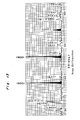
- Fig. 13 is a diffraction chart for showing the measurements of the Y1Ba2Cu3O7-x film by the X-ray diffraction. As apparent from this chart, it can be seen that the superconductor film grows orientated along the c axis from the substrate 7.
- a ceramic superconductive magneto-resistive device 6 was completed.
- the device 6 was 5mm in width, and 10mm in length, and the distance between the voltage electrodes 4 and 5 was 5mm.
- the ceramic superconductive magneto-resistive device 6 was chilled to a liquid nitrogen temperature of 77K at which it was brought into a superconductive state.
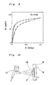
- a magnetic field was applied in an the x axial direction which is perpendicular to the main surface 1a of the superconductive film 1 as shown in Fig. 4, the device 6 showed a hysteresis property of the resistance R in which the resistance R changes different way depending on whether the applied magnetic field H is increasing or decreasing as shown in Fig. 8. Which reference to Fig.
- the reason why the hysterisis property of the resistance R occurs can be considered that the magnetic flux easily passes through the film surface 1a and is caught by the superconductor 1, when the magnetic field is applied to the superconductive film 1 in a direction perpendicular to the surface 1a.
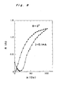
- the resistance R developed in the device 6 showed the same values against the same amount of the magnetic field despite that the applied magnetic field H is increasing or decreasing. Within the permissible errors in measurement, the hysteresis property of the resistance R of the device 6 did not appear.
- the value ⁇ in Fig. 9 represents an angle formed by the direction of the X axis which is perpendicular to the surface 1a of the superconductive film 1 and the direction H of the magnetic field as shown in Fig. 4.
- the above described superconductive magneto-resistive device 6 is an embodiment according to the present invention, and as for the ceramic superconductor, the same effects can be obtained from other film-forming process such as the sputtering process, the MOCVD process or the electron beam deposition process, not only from the spray pyrolisis process.
- this embodiment employs a superconductor of Y-Ba-Cu-O system, other superconductors may be used for obtaining the same effects, for example, superconductors as of Bi-Sr-Ca-Cu-O system, Tl-Ba-Ca-Cu-O system or the like in which the weak coupling of the grains can be formed in the grain boundaries.
- a magnetic field can be measured by the magneto-resistive device composed of a ceramic superconductive film having a high magnetic sensitivity with simple construction and excellent operability. Particularly it is possible to measure the magnetic field with a high accuracy without the effect of the hysteresis of the magneto-resistive by selecting the angle between the superconductor film and an applied magnetic field.
Landscapes
- Physics & Mathematics (AREA)
- Condensed Matter Physics & Semiconductors (AREA)
- General Physics & Mathematics (AREA)
- Superconductor Devices And Manufacturing Methods Thereof (AREA)
- Measuring Magnetic Variables (AREA)
Applications Claiming Priority (2)
| Application Number | Priority Date | Filing Date | Title |
|---|---|---|---|
| JP177456/88 | 1988-07-15 | ||
| JP63177456A JPH0227279A (ja) | 1988-07-15 | 1988-07-15 | 超電導磁気測定装置 |
Publications (3)
| Publication Number | Publication Date |
|---|---|
| EP0350959A2 true EP0350959A2 (de) | 1990-01-17 |
| EP0350959A3 EP0350959A3 (en) | 1990-11-07 |
| EP0350959B1 EP0350959B1 (de) | 1995-01-04 |
Family
ID=16031260
Family Applications (1)
| Application Number | Title | Priority Date | Filing Date |
|---|---|---|---|
| EP89112984A Expired - Lifetime EP0350959B1 (de) | 1988-07-15 | 1989-07-14 | Gerät und Verfahren zum magnetischen Messen mit einer supraleitenden magnetoresistiven Vorrichtung |
Country Status (4)
| Country | Link |
|---|---|
| US (1) | US5126668A (de) |
| EP (1) | EP0350959B1 (de) |
| JP (1) | JPH0227279A (de) |
| DE (1) | DE68920369T2 (de) |
Cited By (2)
| Publication number | Priority date | Publication date | Assignee | Title |
|---|---|---|---|---|
| EP0459679A1 (de) * | 1990-05-21 | 1991-12-04 | Sharp Kabushiki Kaisha | System zum Messen eines Magnetfeldes mit Hilfe eines Supraleitermagnetwiderstandselementes |
| US5447643A (en) * | 1993-01-20 | 1995-09-05 | Huels Aktiengesellschaft | Aqueous fabric softener for the treatment of textile |
Families Citing this family (3)
| Publication number | Priority date | Publication date | Assignee | Title |
|---|---|---|---|---|
| US5673001A (en) * | 1995-06-07 | 1997-09-30 | Motorola, Inc. | Method and apparatus for amplifying a signal |
| US8119187B2 (en) * | 2003-12-15 | 2012-02-21 | Superpower, Inc. | Chemical vapor deposition process using novel precursors |
| JP4985522B2 (ja) * | 2008-03-28 | 2012-07-25 | Tdk株式会社 | 磁界測定方法及び磁気センサ |
Family Cites Families (3)
| Publication number | Priority date | Publication date | Assignee | Title |
|---|---|---|---|---|
| US4366494A (en) * | 1980-05-20 | 1982-12-28 | Rikagaku Kenkyusho | Josephson junction and a method of making the same |
| US4639806A (en) * | 1983-09-09 | 1987-01-27 | Sharp Kabushiki Kaisha | Thin film magnetic head having a magnetized ferromagnetic film on the MR element |
| DE3884514T2 (de) * | 1987-07-29 | 1994-02-10 | Sharp Kk | Verfahren und Anordnung zum Nachweisen eines Magnetfeldes mittels der Magneto-widerstandseigenschaften eines supraleitenden Materials. |
-
1988
- 1988-07-15 JP JP63177456A patent/JPH0227279A/ja active Pending
-
1989
- 1989-07-14 US US07/380,011 patent/US5126668A/en not_active Expired - Lifetime
- 1989-07-14 EP EP89112984A patent/EP0350959B1/de not_active Expired - Lifetime
- 1989-07-14 DE DE68920369T patent/DE68920369T2/de not_active Expired - Fee Related
Cited By (3)
| Publication number | Priority date | Publication date | Assignee | Title |
|---|---|---|---|---|
| EP0459679A1 (de) * | 1990-05-21 | 1991-12-04 | Sharp Kabushiki Kaisha | System zum Messen eines Magnetfeldes mit Hilfe eines Supraleitermagnetwiderstandselementes |
| US5194808A (en) * | 1990-05-21 | 1993-03-16 | Sharp Kabushiki Kaisha | Magnetic field detector using a superconductor magnetoresistive element with ac and dc biasing and a signal processor using fourier transform |
| US5447643A (en) * | 1993-01-20 | 1995-09-05 | Huels Aktiengesellschaft | Aqueous fabric softener for the treatment of textile |
Also Published As
| Publication number | Publication date |
|---|---|
| EP0350959B1 (de) | 1995-01-04 |
| DE68920369D1 (de) | 1995-02-16 |
| DE68920369T2 (de) | 1995-08-10 |
| EP0350959A3 (en) | 1990-11-07 |
| US5126668A (en) | 1992-06-30 |
| JPH0227279A (ja) | 1990-01-30 |
Similar Documents
| Publication | Publication Date | Title |
|---|---|---|
| Nikolo et al. | Flux creep and activation energies at the grain boundaries of Y-Ba-Cu-O superconductors | |
| Campbell et al. | Flux creep in the critical state of a high-temperature superconductor | |
| Batlogg et al. | Superconducting and normal state parameters of Bi2. 2Sr2Ca0. 8Cu2O8+ δ single crystals: A comparison with Ba2YCu3O7 | |
| US5011818A (en) | Sensing a magnetic field with a super conductive material that exhibits magneto resistive properties | |
| US5126668A (en) | Method of eliminating the effect of hysteresis in a superconductive magneto-resistive device | |
| US5126667A (en) | Superconductive magneto-resistive device for sensing an external magnetic field | |
| Faley et al. | DC-SQUID magnetometers and gradiometers on the basis of quasiplanar ramp-type Josephson junctions | |
| Babic et al. | Critical currents and differential resistance of YBa2Cu3O7-x superconducting ceramics | |
| EP0367416B1 (de) | Supraleitender Apparat, bestehend aus einer luftdicht verpackten supraleitenden Einrichtung | |
| US5254945A (en) | Magneto-resistive superconductive device and method for sensing magnetic fields | |
| Shaulov et al. | Characterization of Y‐Ba‐Cu‐O thin films using their nonlinear magnetic response | |
| EP0349996B1 (de) | Magnetfeldmessgerät mit einem supraleitenden magnetoresistiven Element | |
| JP2936125B2 (ja) | 磁気方位検出方法 | |
| Walia et al. | Superconductivity in BiSrCaCuO films made by spray pyrolysis | |
| JP2936126B2 (ja) | 磁気方位の検出可能な磁気センサ | |
| EP0406024B1 (de) | Verfahren und Gerät zum Feststellen eines magnetischen Feldes mit einer Magnetwiderstandseigenschaft eines supraleitenden Materials | |
| JP2933681B2 (ja) | 磁界の測定方法 | |
| Fuller-Mora | Angular dependence of I c (H) in Bi 2 Sr 2 Ca 2 Cu 3 O x tapes | |
| Nojima et al. | Fundamental characteristics of a magnetoresistive sensor using Y/sub 1/Ba/sub 2/Cu/sub 3/O/sub 7-x/ceramic superconducting films | |
| Grishin et al. | Anomalous response of YBCO films to ultraweak magnetic fields | |
| Ousset et al. | 2D Conductivity in the Normal State of the 123 Superconducting Copper Oxides. Experimental Proof on GdBa2Cu3O7 | |
| Głlowacki et al. | Hall probe Cdx Hg1-x Te for use in magnetic investigations of Nb3Sn superconducting layers | |
| Flippen et al. | AC inductance measurements of high-temperature superconductor thin films in DC magnetic fields | |
| Ciszek et al. | Determination of the Superconducting Transition Onset Temperature in Small-Volume Specimens | |
| JP3005628B2 (ja) | 磁界強さ測定方法 |
Legal Events
| Date | Code | Title | Description |
|---|---|---|---|
| PUAI | Public reference made under article 153(3) epc to a published international application that has entered the european phase |
Free format text: ORIGINAL CODE: 0009012 |
|
| AK | Designated contracting states |
Kind code of ref document: A2 Designated state(s): CH DE FR GB IT LI NL |
|
| PUAL | Search report despatched |
Free format text: ORIGINAL CODE: 0009013 |
|
| AK | Designated contracting states |
Kind code of ref document: A3 Designated state(s): CH DE FR GB IT LI NL |
|
| 17P | Request for examination filed |
Effective date: 19901219 |
|
| 17Q | First examination report despatched |
Effective date: 19921130 |
|
| GRAA | (expected) grant |
Free format text: ORIGINAL CODE: 0009210 |
|
| AK | Designated contracting states |
Kind code of ref document: B1 Designated state(s): CH DE FR GB IT LI NL |
|
| PG25 | Lapsed in a contracting state [announced via postgrant information from national office to epo] |
Ref country code: IT Free format text: LAPSE BECAUSE OF FAILURE TO SUBMIT A TRANSLATION OF THE DESCRIPTION OR TO PAY THE FEE WITHIN THE PRESCRIBED TIME-LIMIT;WARNING: LAPSES OF ITALIAN PATENTS WITH EFFECTIVE DATE BEFORE 2007 MAY HAVE OCCURRED AT ANY TIME BEFORE 2007. THE CORRECT EFFECTIVE DATE MAY BE DIFFERENT FROM THE ONE RECORDED. Effective date: 19950104 Ref country code: NL Effective date: 19950104 Ref country code: CH Effective date: 19950104 Ref country code: LI Effective date: 19950104 |
|
| REF | Corresponds to: |
Ref document number: 68920369 Country of ref document: DE Date of ref document: 19950216 |
|
| ET | Fr: translation filed | ||
| REG | Reference to a national code |
Ref country code: CH Ref legal event code: PL |
|
| NLV1 | Nl: lapsed or annulled due to failure to fulfill the requirements of art. 29p and 29m of the patents act | ||
| PLBE | No opposition filed within time limit |
Free format text: ORIGINAL CODE: 0009261 |
|
| STAA | Information on the status of an ep patent application or granted ep patent |
Free format text: STATUS: NO OPPOSITION FILED WITHIN TIME LIMIT |
|
| 26N | No opposition filed | ||
| REG | Reference to a national code |
Ref country code: GB Ref legal event code: IF02 |
|
| PGFP | Annual fee paid to national office [announced via postgrant information from national office to epo] |
Ref country code: FR Payment date: 20020709 Year of fee payment: 14 |
|
| PGFP | Annual fee paid to national office [announced via postgrant information from national office to epo] |
Ref country code: GB Payment date: 20020710 Year of fee payment: 14 |
|
| PGFP | Annual fee paid to national office [announced via postgrant information from national office to epo] |
Ref country code: DE Payment date: 20020717 Year of fee payment: 14 |
|
| PG25 | Lapsed in a contracting state [announced via postgrant information from national office to epo] |
Ref country code: GB Free format text: LAPSE BECAUSE OF NON-PAYMENT OF DUE FEES Effective date: 20030714 |
|
| PG25 | Lapsed in a contracting state [announced via postgrant information from national office to epo] |
Ref country code: DE Free format text: LAPSE BECAUSE OF NON-PAYMENT OF DUE FEES Effective date: 20040203 |
|
| GBPC | Gb: european patent ceased through non-payment of renewal fee |
Effective date: 20030714 |
|
| PG25 | Lapsed in a contracting state [announced via postgrant information from national office to epo] |
Ref country code: FR Free format text: LAPSE BECAUSE OF NON-PAYMENT OF DUE FEES Effective date: 20040331 |
|
| REG | Reference to a national code |
Ref country code: FR Ref legal event code: ST |