EP0351299A1 - Verfahren zur Herstellung eines elektrischen Hochspannungskondensators und Kondensator - Google Patents
Verfahren zur Herstellung eines elektrischen Hochspannungskondensators und Kondensator Download PDFInfo
- Publication number
- EP0351299A1 EP0351299A1 EP89401975A EP89401975A EP0351299A1 EP 0351299 A1 EP0351299 A1 EP 0351299A1 EP 89401975 A EP89401975 A EP 89401975A EP 89401975 A EP89401975 A EP 89401975A EP 0351299 A1 EP0351299 A1 EP 0351299A1
- Authority
- EP
- European Patent Office
- Prior art keywords
- type
- capacitor
- reconstituted mica
- dielectric material
- layer
- Prior art date
- Legal status (The legal status is an assumption and is not a legal conclusion. Google has not performed a legal analysis and makes no representation as to the accuracy of the status listed.)
- Withdrawn
Links
- 239000003990 capacitor Substances 0.000 title claims abstract description 73
- 238000000034 method Methods 0.000 title claims abstract description 45
- 239000010445 mica Substances 0.000 claims abstract description 60
- 229910052618 mica group Inorganic materials 0.000 claims abstract description 60
- 238000005470 impregnation Methods 0.000 claims abstract description 8
- 229920005989 resin Polymers 0.000 claims abstract description 7
- 239000011347 resin Substances 0.000 claims abstract description 7
- 239000004020 conductor Substances 0.000 claims abstract description 5
- 239000011159 matrix material Substances 0.000 claims abstract description 5
- 238000010438 heat treatment Methods 0.000 claims abstract description 4
- 239000003989 dielectric material Substances 0.000 claims description 39
- 238000004078 waterproofing Methods 0.000 claims description 18
- 239000000463 material Substances 0.000 claims description 17
- 239000002985 plastic film Substances 0.000 claims description 11
- 229920006255 plastic film Polymers 0.000 claims description 11
- 238000007650 screen-printing Methods 0.000 claims description 11
- 238000004519 manufacturing process Methods 0.000 claims description 8
- 239000002131 composite material Substances 0.000 claims description 7
- 229910052751 metal Inorganic materials 0.000 claims description 7
- 239000002184 metal Substances 0.000 claims description 7
- 238000005520 cutting process Methods 0.000 claims description 6
- 238000006116 polymerization reaction Methods 0.000 claims description 6
- 238000000151 deposition Methods 0.000 claims description 5
- 239000011521 glass Substances 0.000 claims description 5
- 238000001465 metallisation Methods 0.000 claims description 5
- -1 polypropylene, phenylene Polymers 0.000 claims description 5
- 239000000919 ceramic Substances 0.000 claims description 4
- 230000008021 deposition Effects 0.000 claims description 3
- 239000004033 plastic Substances 0.000 claims description 3
- 150000001875 compounds Chemical class 0.000 claims description 2
- 230000003750 conditioning effect Effects 0.000 claims description 2
- 229920000515 polycarbonate Polymers 0.000 claims description 2
- 239000004417 polycarbonate Substances 0.000 claims description 2
- 229920000728 polyester Polymers 0.000 claims description 2
- 229920001021 polysulfide Polymers 0.000 claims description 2
- 239000005077 polysulfide Substances 0.000 claims description 2
- 150000008117 polysulfides Polymers 0.000 claims description 2
- 229920001343 polytetrafluoroethylene Polymers 0.000 claims description 2
- 239000004810 polytetrafluoroethylene Substances 0.000 claims description 2
- 239000011888 foil Substances 0.000 claims 1
- 230000001143 conditioned effect Effects 0.000 abstract 2
- 239000000976 ink Substances 0.000 description 9
- 238000004804 winding Methods 0.000 description 5
- BQCADISMDOOEFD-UHFFFAOYSA-N Silver Chemical compound [Ag] BQCADISMDOOEFD-UHFFFAOYSA-N 0.000 description 3
- 229910052709 silver Inorganic materials 0.000 description 3
- 239000004332 silver Substances 0.000 description 3
- 239000011230 binding agent Substances 0.000 description 2
- 230000007547 defect Effects 0.000 description 2
- 238000001035 drying Methods 0.000 description 2
- 238000005245 sintering Methods 0.000 description 2
- 101100148830 Arabidopsis thaliana SCI1 gene Proteins 0.000 description 1
- LCFVJGUPQDGYKZ-UHFFFAOYSA-N Bisphenol A diglycidyl ether Chemical compound C=1C=C(OCC2OC2)C=CC=1C(C)(C)C(C=C1)=CC=C1OCC1CO1 LCFVJGUPQDGYKZ-UHFFFAOYSA-N 0.000 description 1
- RYGMFSIKBFXOCR-UHFFFAOYSA-N Copper Chemical compound [Cu] RYGMFSIKBFXOCR-UHFFFAOYSA-N 0.000 description 1
- 239000004593 Epoxy Substances 0.000 description 1
- 101100054266 Saccharomyces cerevisiae (strain ATCC 204508 / S288c) SNF4 gene Proteins 0.000 description 1
- 238000004026 adhesive bonding Methods 0.000 description 1
- 230000032683 aging Effects 0.000 description 1
- 229910052782 aluminium Inorganic materials 0.000 description 1
- XAGFODPZIPBFFR-UHFFFAOYSA-N aluminium Chemical compound [Al] XAGFODPZIPBFFR-UHFFFAOYSA-N 0.000 description 1
- 239000003985 ceramic capacitor Substances 0.000 description 1
- 239000011248 coating agent Substances 0.000 description 1
- 238000000576 coating method Methods 0.000 description 1
- 238000007796 conventional method Methods 0.000 description 1
- 238000010411 cooking Methods 0.000 description 1
- 229910052802 copper Inorganic materials 0.000 description 1
- 239000010949 copper Substances 0.000 description 1
- 238000005516 engineering process Methods 0.000 description 1
- 239000003822 epoxy resin Substances 0.000 description 1
- 238000010304 firing Methods 0.000 description 1
- 238000007667 floating Methods 0.000 description 1
- 230000006870 function Effects 0.000 description 1
- 150000002739 metals Chemical class 0.000 description 1
- 238000004806 packaging method and process Methods 0.000 description 1
- 239000002245 particle Substances 0.000 description 1
- 230000035515 penetration Effects 0.000 description 1
- 229920002492 poly(sulfone) Polymers 0.000 description 1
- 229920000647 polyepoxide Polymers 0.000 description 1
- 229920001225 polyester resin Polymers 0.000 description 1
- 239000004645 polyester resin Substances 0.000 description 1
- 239000002861 polymer material Substances 0.000 description 1
- 229920002050 silicone resin Polymers 0.000 description 1
- 238000004513 sizing Methods 0.000 description 1
- 238000005507 spraying Methods 0.000 description 1
- 239000000126 substance Substances 0.000 description 1
Images

Classifications
-
- H—ELECTRICITY
- H01—ELECTRIC ELEMENTS
- H01G—CAPACITORS; CAPACITORS, RECTIFIERS, DETECTORS, SWITCHING DEVICES, LIGHT-SENSITIVE OR TEMPERATURE-SENSITIVE DEVICES OF THE ELECTROLYTIC TYPE
- H01G4/00—Fixed capacitors; Processes of their manufacture
- H01G4/002—Details
- H01G4/018—Dielectrics
- H01G4/20—Dielectrics using combinations of dielectrics from more than one of groups H01G4/02 - H01G4/06
- H01G4/22—Dielectrics using combinations of dielectrics from more than one of groups H01G4/02 - H01G4/06 impregnated
-
- H—ELECTRICITY
- H01—ELECTRIC ELEMENTS
- H01G—CAPACITORS; CAPACITORS, RECTIFIERS, DETECTORS, SWITCHING DEVICES, LIGHT-SENSITIVE OR TEMPERATURE-SENSITIVE DEVICES OF THE ELECTROLYTIC TYPE
- H01G4/00—Fixed capacitors; Processes of their manufacture
- H01G4/30—Stacked capacitors
Definitions
- the present invention relates to a method for manufacturing a high-voltage electric capacitor.
- the latter According to the most common current technique for manufacturing high-voltage capacitors, it is advantageous to produce the latter from a ribbon or film of dielectric material such as a reconstituted mica designated by "micapaper" in English language, this film being wound together with a corresponding metal sheet placed on each side of the reconstituted mica sheet. Each metal sheet is provided with tabs allowing, after metallization, to form the contact terminals of the capacitor.
- the reconstituted mica is normally commercially available in sheets whose thickness is between 18 ⁇ m and 50 ⁇ m, these sheets consisting of a planar arrangement of powdered mica particles whose cohesion is ensured solely by Van der Wall forces. This type of product is manufactured and distributed in the United States of America.
- a drying of the winding, or winding thus obtained is carried out, followed by impregnation using an epoxy resin, a polyester resin or a silicone resin and a corresponding polymerization depending on the application or the use of the capacitor in question.
- the capacitors thus obtained exhibit good voltage withstand due to the dielectric properties of mica, and good resistance to the phenomenon of aging.
- a first approach using the aforementioned traditional technique, can consist in using better quality impregnation materials and in reducing the thickness of the dielectric material.
- this solution has the drawback of causing an increase in voltage gradient and a consequent decrease in the reliability of the capacitors thus obtained, due to the risks of greater defects in the substance of the dielectric material.
- the actual winding mode causes disturbances in the structure of the dielectric material, in particular for the small radii of curvature of the winding, which causes defects in voltage resistance.
- This same winding mode also causes losses of capacity actually obtained, due to the existence of an expansion coefficient between real and theoretical capacity.
- raw mica as a dielectric material, also called clear mica
- the aforementioned limitations result in the impossibility of using capacitors whose capacity is greater than 47 nF and whose operating voltage is greater than 5 KV.
- the present invention aims to remedy the aforementioned drawbacks by applying a new technique to the dielectric material such as reconstituted mica.
- Another object of the present invention is the implementation, in accordance with the aforementioned technique, of high-voltage electric capacitors for which the gain in density of stored energy is greater than 25%.
- Another object of the present invention is the implementation, in accordance with the aforementioned technique, of high-voltage capacitors having characteristics adapted according to the use considered.
- the process for manufacturing a high-voltage electric capacitor which is the subject of the invention is remarkable in that it consists: to condition a plurality of sheets of dielectric material of the reconstituted mica type; - To form on at least one face of each sheet of the dielectric material an electrically conductive area so as to constitute an electrode of first type or of second type for the capacitor; - Stacking, in a forming matrix, a plurality of said sheets of reconstituted mica, two successive electrodes of different type being, in the stack formed, separated by at least one thickness of a sheet of reconstituted mica; - subjecting the stack of reconstituted mica sheets to a heat treatment and to a pressure so as to condition the stack in a substantially homogeneous block; - subjecting said substantially homogeneous block to an impregnation by means of a polymerizable resin; - subjecting the substantially homogeneous block impregnated with polymerization to obtain a final block; - To make a supply of electrically conductive material to connect on the one
- the high-voltage electric capacitor object of the invention is remarkable in that it is formed by a stack of a plurality of stacked layers of dielectric material in mica recons titled, each successive layer being separated from the next by at least one electrically conductive wafer forming an electrode of a first or a second type, the electrodes of the first, respectively of the second type, being each interconnected to each form the contact terminals of said capacitor.
- the high-voltage electric capacitor that is the subject of the invention finds application in any industrial electronics, airborne, atmospheric or space electronics device.
- the process for manufacturing a high-voltage electric capacitor that is the subject of the invention consists in conditioning a plurality of sheets, denoted FE, of dielectric material, this dielectric material being constituted by reconstituted mica.
- a particularly advantageous non-limiting mode of packaging for the implementation of the process which is the subject of the invention consists, for example, as shown in point a) of FIG. 1, of gluing a support frame denoted CS, constituted for example by a frame hollow of substantially square shape, on which is applied a sheet FE of mica reconstituted from a roll of MRC mica.
- the application of the sheet of FE mica on the frame CS then makes it possible, using a cutting tool OD, to prepare a set consisting of the support frame CS covered with a sheet of reconstituted mica FE.
- the dimensions of the support frame CS and of the sheet FE are adapted accordingly.
- the process which is the subject of the invention then consists in forming on at least one face of each sheet FE of the dielectric material constituted by the reconstituted mica, a zone electrically conductive marked ZE1 or ZE2.
- the electrically conductive zones ZE1, ZE2 are formed so as to constitute an electrode of a first or of a second type for the capacitor considered.
- These zones ZE1, ZE2 have a geometry adapted to the shape of the capacitor to be produced. They can usually have a rectangular, square or circular shape.
- the electrically conductive zones ZE1, ZE2 are shown having an asymmetric overflow on one of the sides of the sheet of dielectric material FE mounted on the support frame CS, each overflow flush with the aforementioned side FE sheet to form the contact area of the electrically conductive area with the corresponding contact terminal of the capacitor formed later.
- the process which is the subject of the invention does not prejudge the production of electrodes of the first or second types alone, but may also consist in producing a floating type electrode in accordance with the usual technique for producing ceramic capacitors for example.
- electrically conductive zones ZE1 or ZE2 can advantageously, in accordance with the method which is the subject of the invention, be produced by intermediate stacking of an electrically conductive sheet, an aluminum sheet for example.
- the electrically conductive zones ZE1 or ZE2 can be produced by screen printing using an electrically conductive ink.
- screen printing consists in depositing a conductive ink based on silver and an organic binder on the corresponding electrically conductive zone ZE1 or ZE2.
- Commonly used inks may include a silver solution suspended with organic binders and a sintering glass.
- Conventional screen printing techniques can then be used, these consisting, following the deposition of the aforementioned ink, in producing the pattern corresponding to the electrically conductive zone ZE1 or ZE2 through a screen, in a conventional manner.
- the deposition of the ink in accordance with the pattern corresponding to the aforementioned electrically conductive area is then followed by a firing step, the screen-printed pattern and the sheet of dielectric material FE then being subjected to the support frame CS, to a cooking step at a temperature which can vary between 400 and 550 ° C.
- each sheet FE of the dielectric material of an electrically conductive area the process which is the subject of the invention then consists, as well as represented in point c) of FIG. 1, to be stacked in a forming matrix denoted MF, a plurality of the sheets of reconstituted mica FE provided with their electrically conductive zones ZE1 of the first type or ZE2 of the second type.
- a forming matrix denoted MF a forming matrix denoted MF
- two successive electrodes of different type that is to say of the first or of the second type, are in the stack formed, separated by at least one thickness of a sheet of reconstituted mica.
- a particularly advantageous nonlimiting operating mode consists for example in placing each support frame CS directly above the forming matrix MF to ensure, using 'A punch PO, the successive cutting and stacking of each sheet of reconstituted mica FE provided with the electrically conductive zone ZE1 or ZE2 consisting of the electrode of the first or second type respectively.
- it is advantageous to end with one or more non-screen-printed sheets so as to protect the screen-printed sheets ending the stack.
- this then consists, as shown in point d) of FIG. 1, in subjecting the stack of reconstituted mica sheets thus formed, to a heat treatment denoted T ° and to a pressure P so as to condition the stack in a substantially homogeneous block.
- Treatment by temperature T ° and by pressurization makes it possible to sinter the glasses contained in the screen printing ink.
- the aforementioned sintering temperature T ° can be between 200 ° C and 1300 ° C approximately.
- the aforementioned stack, obtained following step d of the method object of the invention is in the form of a homogeneous parallelepiped containing, depending on the screen printing patterns used, one or more capacitors.
- the process which is the subject of the invention then consists in subjecting the above-mentioned substantially homogeneous block to an impregnation, by means of a polymerizable resin, the substantially homogeneous impregnated block then being subjected to a temperature treatment to carry out the polymerization of the resin.
- the substantially homogeneous blocks can be mounted in a ventilated oven, then in a vacuum oven to ensure drying, the impregnation being carried out by means of an epoxy type resin for example, of the type DGEBA, and the polymerization being carried out accordingly according to conventional techniques depending on the resin used.
- the polymerization step shown in point e of Figure 1 provides a final block.
- the final block is then cut, the cutting being carried out of course according to the patterns of the electrically conductive areas actually produced.
- This cutting can be carried out for example using a sawing machine X, Y in advance step by step or using any conventional means.
- the cutting step is represented in point f) of FIG. 1 and makes it possible to obtain a plurality of elementary blocks, each elementary block potentially constituting a capacitor.
- the process which is the subject of the invention then consists, as shown in point g) of FIG. 1, of providing an electrically conductive material to connect on the one hand the electrodes of the first type, and on the other hand the electrodes of the second type, constituted respectively by the electrically conductive zones ZE1 and ZE2 to form, for each elementary block, a capacitor.
- the supply step of electrically conductive material schematically, by a step consisting in ensuring a spraying of molten metal for example, such an operation being commonly designated in the technique of manufacturing capacitors by "shooping".
- any other metallization technique such as for example coating of conductive ink charged with metals, on the corresponding faces of each elementary block, can also be used.
- this prior to the step consisting in forming an electrically conductive zone on at least one face of each sheet of reconstituted mica FE, may also consist in forming, on the sheet or sheets of reconstituted mica FE, a sub-layer SC for waterproofing the reconstituted mica.
- This layer designated by waterproofing layer, makes it possible in fact to further ensure better bonding or bonding between the screen-printed layer, when screen printing is used, and the mica.
- This SC sub-layer has the function in particular of preventing the penetration of the silver, contained in the screen printing ink, into the reconstituted mica. Indeed, this material is porous, especially for reconstituted mica sheets of small thickness, that is to say of thickness between 18 to 20 micrometers approximately.
- the waterproofing sublayer SC can be formed by depositing a layer of a dielectric material whose dielectric constant ⁇ r has a relative value between 3 and 100, 3 ⁇ ⁇ r ⁇ 100.
- the waterproofing layer SC can be a waterproofing layer total or partial, the material used to produce the aforementioned waterproofing layer SC may consist of a glass such as a lead borosilicate, a polymer material, a ceramic or a plastic material.
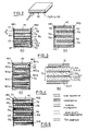
- FIG. 3a there is shown a capacitor obtained by implementing the method which is the subject of the invention, according to a first non-limiting embodiment.
- the capacitor shown in the above figure in a sectional view along a longitudinal plane of symmetry, is formed of a stack of a plurality of layers denoted Ci, of dielectric material in reconstituted mica.
- Each successive layer Ci is separated from the following Ci + 1 by at least one section denoted Ti electrically conductive forming the electrodes of the first respectively second type E1, E2.
- the electrodes of the first respectively second type E1, E3, E5, E7 and E2, E4, E6, the odd index designating the electrodes of the first type and the index even the electrodes of the second type, are each interconnected to each form the contact terminals ME1 and ME2 respectively of the capacitor.
- the capacitor is embedded in the impregnation material denoted MI.
- two successive electrodes of opposite type, E1 and E2 for example, or of the first and second types, are separated in the stack by at least one layer of dielectric material of reconstituted mica .
- each layer Ci of dielectric material of reconstituted mica each comprise an electrode of the first or of the second type, the electrodes of the same layer Ci being of opposite type, ie of the first and second types.
- two successive electrodes of opposite type are separated in the stack by at least one layer of reconstituted mica material, but two electrodes of the same type , electrodes E2 and E4 for example, are on the contrary in direct contact, these two electrodes being on the other hand connected to the contact terminal ME2 of the capacitor.
- the electrodes can be formed by an electrically conductive ink applied by screen printing, as described above for the implementation of the process which is the subject of the invention, or by an intermediate metal sheet inserted during the stacking of the layers Ci.
- FIGS. 4a and 4b An advantageous alternative embodiment of a capacitor which is the subject of the invention will be described in connection with FIGS. 4a and 4b.
- the stack further comprises between each electrode of one or the other type and the corresponding face of the layer of dielectric material of reconstituted mica, that is to say for example between the electrodes E1 and E2 and the corresponding face of the layer of dielectric material in reconstituted mica C1, a waterproofing sublayer denoted SCI1 of the reconstituted mica.
- each layer Ci is thus provided with one or more sub-layers, on each corresponding face, for waterproofing.
- Each SCIi waterproofing sublayer is advantageously made of a dielectric material whose dielectric constant ⁇ r has a relative value between 3 and 100, 3 ⁇ ⁇ r ⁇ 100.
- the dielectric material constituting the SCIi waterproofing sublayer is a material such as for example a glass, a lead borosilicate compound, a polymeric material or a ceramic.
- the waterproofing underlay may have a thickness of between 1.5 and 12 micrometers depending on the chosen thickness of the layer of reconstituted mica Ci. The choice of the nature of the material constituting the waterproofing underlay SCIi is then guided according to the use of the capacitor obtained in accordance with the object of the present invention. For obtaining capacitors of very high capacity, it will be possible to use dielectric materials having a very high relative dielectric constant, material such as ceramic for example.
- each layer Ci of dielectric material in reconstituted mica can be formed, without limitation, of a plurality of elementary composite layers denoted CiEkc constituting in fact the layer of reconstituted mica Ci.
- each elementary composite layer is formed by a stack of an elementary layer of dielectric material in reconstituted mica denoted CiEk1 comprising, on at least one of these faces, an elementary waterproofing sub-layer denoted CiEk2 respectively CiEk3.
- the layer of dielectric material Ci thus formed of a plurality of elementary composite layers can then comprise an electrode of a first type denoted Ei in FIG. 4b and an electrode of a second type denoted Ei + 1 on this same figure.
- each layer of dielectric material of reconstituted mica is formed of a plurality of elementary composite layers can advantageously be used when producing capacitors in accordance with the object of the present invention having layers of reconstituted mica material; these layers are then produced by superimposing a plurality of elementary composite layers.
- FIG. 5 Another nonlimiting alternative embodiment of a capacitor in accordance with the object of the present invention will be described in conjunction with FIG. 5.
- the electrodes E1, E2 of a first or of a second type can be formed by means of a plastic film denoted FP1, FP2 metallized.
- the plastic film then comprises a metallization on at least one of its faces to constitute an electrode of the first or of the second type.
- the plastic film comprising the aforementioned metallizations is then introduced, during the constitution of the stack, in a manner analogous to the method described above, in the case of the use of screen-printed electrodes for example.
- the metallized plastic films are introduced for example in place of the metal sheets intended to constitute the armature of the capacitor.
- the metallized plastic film FP1, FP2 can be a plastic film chosen from the group of plastic materials such as polycarbonate, polyester, polypropylene, phenylene polysulfide, polysulfone, polytetrafluoroethylene for example.
- the aforementioned plastic films can have a thickness of the order of 1.5 micrometers to 2 micrometers. It will be understood that, in this case, the plastic film FP1 or FP2 then plays the role of the waterproofing sublayer.
- Figure 5 there is shown a legend of the representation of the materials used for the implementation of the capacitors in accordance with the object of the invention, in the various embodiments.
Landscapes
- Engineering & Computer Science (AREA)
- Power Engineering (AREA)
- Manufacturing & Machinery (AREA)
- Microelectronics & Electronic Packaging (AREA)
- Fixed Capacitors And Capacitor Manufacturing Machines (AREA)
Applications Claiming Priority (2)
| Application Number | Priority Date | Filing Date | Title |
|---|---|---|---|
| FR8809456A FR2634314B1 (fr) | 1988-07-12 | 1988-07-12 | Procede de fabrication d'un condensateur electrique haute tension et condensateur ainsi obtenu |
| FR8809456 | 1988-07-12 |
Publications (1)
| Publication Number | Publication Date |
|---|---|
| EP0351299A1 true EP0351299A1 (de) | 1990-01-17 |
Family
ID=9368356
Family Applications (1)
| Application Number | Title | Priority Date | Filing Date |
|---|---|---|---|
| EP89401975A Withdrawn EP0351299A1 (de) | 1988-07-12 | 1989-07-10 | Verfahren zur Herstellung eines elektrischen Hochspannungskondensators und Kondensator |
Country Status (2)
| Country | Link |
|---|---|
| EP (1) | EP0351299A1 (de) |
| FR (1) | FR2634314B1 (de) |
Citations (4)
| Publication number | Priority date | Publication date | Assignee | Title |
|---|---|---|---|---|
| FR1328877A (fr) * | 1961-07-19 | 1963-05-31 | Johnson Matthey Co Ltd | Perfectionnement aux condensateurs électriques |
| US3229173A (en) * | 1961-01-10 | 1966-01-11 | Cornell Dubilier Electric | Mica condenser with hard-metal terminal foils and lead-tin foil connections to the electrodes |
| FR2389211A1 (fr) * | 1977-04-26 | 1978-11-24 | Eurofarad | Fabrication de condensateurs a dielectrique mica multicouches, avec interposition de couches de verre |
| FR2608311A1 (fr) * | 1986-12-16 | 1988-06-17 | Europ Composants Electron | Condensateur a film plastique metallise, a coefficient de temperature defini et a bonne stabilite dans le temps |
Family Cites Families (1)
| Publication number | Priority date | Publication date | Assignee | Title |
|---|---|---|---|---|
| US3275914A (en) * | 1963-09-19 | 1966-09-27 | Sangamo Electric Co | Electric capacitor having dielectric spacer of reconstituted mica interleaved with solid plastic |
-
1988
- 1988-07-12 FR FR8809456A patent/FR2634314B1/fr not_active Expired - Lifetime
-
1989
- 1989-07-10 EP EP89401975A patent/EP0351299A1/de not_active Withdrawn
Patent Citations (4)
| Publication number | Priority date | Publication date | Assignee | Title |
|---|---|---|---|---|
| US3229173A (en) * | 1961-01-10 | 1966-01-11 | Cornell Dubilier Electric | Mica condenser with hard-metal terminal foils and lead-tin foil connections to the electrodes |
| FR1328877A (fr) * | 1961-07-19 | 1963-05-31 | Johnson Matthey Co Ltd | Perfectionnement aux condensateurs électriques |
| FR2389211A1 (fr) * | 1977-04-26 | 1978-11-24 | Eurofarad | Fabrication de condensateurs a dielectrique mica multicouches, avec interposition de couches de verre |
| FR2608311A1 (fr) * | 1986-12-16 | 1988-06-17 | Europ Composants Electron | Condensateur a film plastique metallise, a coefficient de temperature defini et a bonne stabilite dans le temps |
Also Published As
| Publication number | Publication date |
|---|---|
| FR2634314A1 (fr) | 1990-01-19 |
| FR2634314B1 (fr) | 1990-10-19 |
Similar Documents
| Publication | Publication Date | Title |
|---|---|---|
| US10176923B2 (en) | Ceramic electronic component and method of producing the same | |
| US6358570B1 (en) | Vacuum deposition and curing of oligomers and resins | |
| US5260095A (en) | Vacuum deposition and curing of liquid monomers | |
| EP1347476B1 (de) | Keramisches elektronikbauteil und dessen herstellungsverfahren | |
| KR102366445B1 (ko) | 적층 세라믹 전자부품 | |
| US20090310276A1 (en) | Multilayer ceramic electronic component and method for manufacturing the same | |
| CN110828169B (zh) | 多层陶瓷电容器及制造多层陶瓷电容器的方法 | |
| CN110828171B (zh) | 多层陶瓷电容器及制造多层陶瓷电容器的方法 | |
| FR2807612A1 (fr) | Substrat en ceramique monolithique, son procede de conception et de fabrication et dispositif electronique l'utilisant | |
| CN103515090A (zh) | 多层陶瓷电子元件及其制造方法 | |
| CN113228385B (zh) | 制造电池的方法和由该方法制得的电池 | |
| FR2781601A1 (fr) | Piece electronique en ceramique et son procede de production | |
| FR2567679A1 (fr) | Procede de fabrication d'un condensateur electrolytique solide et condensateur obtenu | |
| US3855507A (en) | Self heating capacitors | |
| US5514326A (en) | Copper paste for internal conductor of multilayer ceramic electronic component | |
| US2731706A (en) | Manufacture of capacitors | |
| EP0034102B1 (de) | Integrierter Spannungsvervielfacher | |
| CN110875136A (zh) | 多层陶瓷电容器及制造多层陶瓷电容器的方法 | |
| CN103597563A (zh) | 层叠陶瓷电子部件的制造方法 | |
| US20020026978A1 (en) | Multilayer ceramic substrate and manufacturing method therefor | |
| JPH11340081A (ja) | 積層セラミック電子部品及びその製造方法 | |
| WO2005036571A1 (ja) | 電極ペースト、セラミック電子部品及びその製造方法 | |
| JPH09106925A (ja) | 積層セラミックコンデンサの製造方法 | |
| EP0351299A1 (de) | Verfahren zur Herstellung eines elektrischen Hochspannungskondensators und Kondensator | |
| CN110544585B (zh) | 多层陶瓷电子组件及制造多层陶瓷电子组件的方法 |
Legal Events
| Date | Code | Title | Description |
|---|---|---|---|
| PUAI | Public reference made under article 153(3) epc to a published international application that has entered the european phase |
Free format text: ORIGINAL CODE: 0009012 |
|
| AK | Designated contracting states |
Kind code of ref document: A1 Designated state(s): DE GB IT |
|
| 17P | Request for examination filed |
Effective date: 19900618 |
|
| 17Q | First examination report despatched |
Effective date: 19920721 |
|
| STAA | Information on the status of an ep patent application or granted ep patent |
Free format text: STATUS: THE APPLICATION IS DEEMED TO BE WITHDRAWN |
|
| 18D | Application deemed to be withdrawn |
Effective date: 19930301 |