EP0351331A1 - Integrierte Schaltungsstruktur, die die Isolation zwischen Bauelementen verbessert - Google Patents
Integrierte Schaltungsstruktur, die die Isolation zwischen Bauelementen verbessert Download PDFInfo
- Publication number
- EP0351331A1 EP0351331A1 EP89420246A EP89420246A EP0351331A1 EP 0351331 A1 EP0351331 A1 EP 0351331A1 EP 89420246 A EP89420246 A EP 89420246A EP 89420246 A EP89420246 A EP 89420246A EP 0351331 A1 EP0351331 A1 EP 0351331A1
- Authority
- EP
- European Patent Office
- Prior art keywords
- type
- conductivity
- substrate
- layer
- circuit structure
- Prior art date
- Legal status (The legal status is an assumption and is not a legal conclusion. Google has not performed a legal analysis and makes no representation as to the accuracy of the status listed.)
- Withdrawn
Links
Images

Classifications
-
- H—ELECTRICITY
- H10—SEMICONDUCTOR DEVICES; ELECTRIC SOLID-STATE DEVICES NOT OTHERWISE PROVIDED FOR
- H10W—GENERIC PACKAGES, INTERCONNECTIONS, CONNECTORS OR OTHER CONSTRUCTIONAL DETAILS OF DEVICES COVERED BY CLASS H10
- H10W10/00—Isolation regions in semiconductor bodies between components of integrated devices
- H10W10/01—Manufacture or treatment
- H10W10/031—Manufacture or treatment of isolation regions comprising PN junctions
-
- H—ELECTRICITY
- H10—SEMICONDUCTOR DEVICES; ELECTRIC SOLID-STATE DEVICES NOT OTHERWISE PROVIDED FOR
- H10W—GENERIC PACKAGES, INTERCONNECTIONS, CONNECTORS OR OTHER CONSTRUCTIONAL DETAILS OF DEVICES COVERED BY CLASS H10
- H10W10/00—Isolation regions in semiconductor bodies between components of integrated devices
- H10W10/30—Isolation regions comprising PN junctions
Definitions
- the present invention relates to a new integrated circuit structure improving the isolation between components and more particularly a structure comprising power components and making it possible to improve the isolation of these power components.
- transistors depending on the conditions of use can operate at high current at different times; according to their dimensions, their arrangements and their respective polarities, they can give rise to high currents in the substrate and trigger the operation of parasitic transistors whose gain can be high enough to lead to the destruction of the circuit.
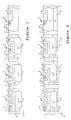
- FIG. 1 represents a conventional integrated circuit structure in which a few specific components have been shown, in cross-section and schematically.
- Reference 1 designates a lateral PNP transistor
- references 2 and 3 of vertical NPN power transistors and reference 4 indicates a PNP substrate transistor.
- These different components are formed in N 10, 20, 30 and 40 type boxes themselves formed in a substrate. 5 of type P and isolated laterally by walls 6 of type P+.
- the lateral PNP transistor 1 consists of a P-type emitter zone 11 surrounded by a P-type collector 12.
- the N-type base contact 13 is outside the collector to avoid recombination in the active base.
- a buried layer 14 is provided to reduce the leakage of the holes towards the substrate.
- the vertical NPN transistors 2 and 3 respectively comprise an emitter zone 21, 31, a base zone 22, 32, and a collector zone formed by the body of the box 20, 30, a collector take-up zone resulting from a buried layer 23, 33, and a collecting well 24, 34 of type N+.
- the substrate PNP transistor 4 comprises a P-type emitter area 41, a base contact recovery area 42 and its collector is formed by the substrate 5.
- the collectors 23, 33 of the contiguous power transistors 2 and 3 will, according to their state of polarization, play the role of emitter and collector of a parasitic lateral NPN transistor whose base is formed by the regions isolation 6 and the substrate 5.
- the first consists in reducing the lifetime of the carriers in the different regions of this transistor by using, for example, a bombardment by electrons or high energy protons (2MeV). Although easy to control, this method does not make it possible to obtain selective control of the different regions and this also results in a reduction in the gain of the active transistors, particularly the lateral PNP transistors (1) and substrate (4), the base of which lightly doped is particularly sensitive to defects created by bombardment.
- an object of the present invention is to provide a new integrated circuit structure improving the isolation between power components in which the bottom of each box containing a component, isolated laterally, dielectrically or by junction, from the other boxes, rests on a diaper additional conductivity type opposite to that of the box formed on a substrate of the same type of conductivity and with a high level of doping.
- FIG. 2 represents an example of parts of bipolar integrated circuits and is identical to FIG. 1 as regards the components formed in the various boxes 10, 20, 30 and 40.
- the same elements and layers are designated by the same reference numerals.
- the various wells instead of being formed on a P-type substrate of low doping level having for example a resistivity of 10 to 20 ohms per centimeter as has been indicated above, are formed in a substrate composed of a main zone 50 heavily doped with P+ type coated with a layer 51 of P type.
- This layer 51 has a doping level equivalent to that of substrate P of P type FIG. 1 to obtain similar voltage withstand characteristics, in particular as regards the junction with layers 23 and 33 of the power transistors 2 and 3 and the base / collector junction of the substrate PNP transistor 4. It will be noted that the walls 6 P+ type with high doping level pass through the P layer 51 to join the P+ type substrate 50.
- FIG. 3A represents a P 50 type substrate 50 on which an epitaxial layer 51 of P type is formed.
- FIG. 3B the same structure is shown as in FIG. 3A with areas marked with crosses 52 consisting of implantations of P-type dopant foundations which completely surround each of the wells which will be subsequently formed.
- crosses 52 consisting of implantations of P-type dopant foundations which completely surround each of the wells which will be subsequently formed.
- N-type layout 53 is made, designated by dots.
- an epitaxial layer of type N 54 is formed above the P 51 type layer. It is moreover possible that during the formation of this epitaxial layer, the implantations 52 and 53 start broadcasting.
- FIG. 3C also shows implantation zones 55 of type P opposite the foundation implantation zones 52.
- Figure 3D shows the structure of Figure 3C after heat treatment.
- the implanted zones 52, 53 and 55 diffuse to form the isolation walls 6 delimiting a box, for example the box 20 of FIGS. 1 and 2 at the bottom of which the buried layer 23 is formed.
- the other manufacturing steps for moving from FIG. 3D to FIG. 2 are conventional steps (it will be noted that in the case where collector wells are formed 24, 34, surface implantations of type N will be made for these wells. the step illustrated in FIG. 3C).
- the particular structure of the substrate used makes it possible to form P-type regions 51 surrounded by P+ regions (substrate 50 and isolation walls 6) at the bottom of each box. These regions P+ prohibit the diffusion of the carriers, electrons in this case, between the two regions N+ which constitute the collectors 23, 33 of the neighboring NPN power transistors 2, 3. It is then possible by an optimal definition of the doping and of the relative dimensions of the regions P 51 and P+ 6 and 50 simultaneously ensuring the voltage withstand required for the isolation diode of the collector of the NPN transistors, diode N+P 23 - 51, and the control of the contribution of the substrate with that of the P+ doping of the base in the operation of the inter-box parasitic lateral NPN transistor.
- the operation of the part of this parasitic lateral NPN transistor formed in the epitaxial layer 54 is also controlled by the doping of its base constituted by the regions P+ forming the foundations and the inter-caisson isolation walls.
- the thickness and the high doping of these regions also makes it possible to reduce the inter-box gain in proportion.
- the substrate structure used, epitaxial layer P on substrate P+, makes it possible to limit the depth of diffusion of the carriers to the epitaxial layer P, the penetration of the isolation foundations in this layer must be sufficient to reduce the lateral path.
- the insulation used to form the wells in the epitaxial layer N can be of the diffused junction type as given by way of example in the case of integration of power components.
- the structure described is also well suited to the integration of large capacity memories, bipolar or MOS.
- the isolation is carried out either by growth of localized oxide, or by etching and filling of grooves carried out in the epitaxial layer of type N in which the boxes 10, 20, 30 and 40 are delimited.
- the present invention applies to the case where the insulation between the boxes is a lateral dielectric isolation and the present invention can be applied to the integration of large capacity memories of bipolar or MOS type.
- the proposed structure can be implemented to reduce the substrate currents and limit, for example, the effects of proximity or crosstalk between memory points when programming programmable large-capacity bipolar read-only memories (256 K) or reduce the influence of particles in dynamic type MOS memories, to improve, for example, the immunity to particles of DRAM type memories with capacitive and large capacity storage (1 to 16 Mbits).
- FIG. 4 illustrates an example of mixed (bipolar-dielectric) isolation between wells.
- Figure 4 shows the same representation as Figure 3D.
- the isolation walls are produced in their lower part by P+ type diffusion resulting from the foundations 52 illustrated in FIG. 3C and in their upper part by an insulated groove 60.
- P+ type diffusion resulting from the foundations 52 illustrated in FIG. 3C and in their upper part by an insulated groove 60.
Landscapes
- Element Separation (AREA)
- Bipolar Integrated Circuits (AREA)
- Bipolar Transistors (AREA)
- Metal-Oxide And Bipolar Metal-Oxide Semiconductor Integrated Circuits (AREA)
Applications Claiming Priority (2)
| Application Number | Priority Date | Filing Date | Title |
|---|---|---|---|
| FR8809848A FR2634321B1 (fr) | 1988-07-13 | 1988-07-13 | Structure de circuit integre ameliorant l'isolement entre composants |
| FR8809848 | 1988-07-13 |
Publications (1)
| Publication Number | Publication Date |
|---|---|
| EP0351331A1 true EP0351331A1 (de) | 1990-01-17 |
Family
ID=9368626
Family Applications (1)
| Application Number | Title | Priority Date | Filing Date |
|---|---|---|---|
| EP89420246A Withdrawn EP0351331A1 (de) | 1988-07-13 | 1989-07-10 | Integrierte Schaltungsstruktur, die die Isolation zwischen Bauelementen verbessert |
Country Status (4)
| Country | Link |
|---|---|
| EP (1) | EP0351331A1 (de) |
| JP (1) | JPH02125636A (de) |
| KR (1) | KR900002445A (de) |
| FR (1) | FR2634321B1 (de) |
Cited By (1)
| Publication number | Priority date | Publication date | Assignee | Title |
|---|---|---|---|---|
| EP0555496A1 (de) * | 1991-07-03 | 1993-08-18 | Consorzio per la Ricerca sulla Microelettronica nel Mezzogiorno - CoRiMMe | Laterale Bipolartransistorstruktur mit integriertem Kontrollschaltkreis und integriertem Leistungstransistor und deren Herstellungsprozess |
Citations (3)
| Publication number | Priority date | Publication date | Assignee | Title |
|---|---|---|---|---|
| DE2952318A1 (de) * | 1979-12-24 | 1981-07-02 | Licentia Patent-Verwaltungs-Gmbh, 6000 Frankfurt | Integrierte schaltungsanordnung |
| EP0057549A2 (de) * | 1981-01-29 | 1982-08-11 | Kabushiki Kaisha Toshiba | Halbleitervorrichtung |
| GB2183907A (en) * | 1985-11-27 | 1987-06-10 | Raytheon Co | Reducing radiation effects on integrated circuits |
-
1988
- 1988-07-13 FR FR8809848A patent/FR2634321B1/fr not_active Expired - Lifetime
-
1989
- 1989-07-10 EP EP89420246A patent/EP0351331A1/de not_active Withdrawn
- 1989-07-12 KR KR1019890009938A patent/KR900002445A/ko not_active Withdrawn
- 1989-07-12 JP JP1180129A patent/JPH02125636A/ja active Pending
Patent Citations (3)
| Publication number | Priority date | Publication date | Assignee | Title |
|---|---|---|---|---|
| DE2952318A1 (de) * | 1979-12-24 | 1981-07-02 | Licentia Patent-Verwaltungs-Gmbh, 6000 Frankfurt | Integrierte schaltungsanordnung |
| EP0057549A2 (de) * | 1981-01-29 | 1982-08-11 | Kabushiki Kaisha Toshiba | Halbleitervorrichtung |
| GB2183907A (en) * | 1985-11-27 | 1987-06-10 | Raytheon Co | Reducing radiation effects on integrated circuits |
Cited By (1)
| Publication number | Priority date | Publication date | Assignee | Title |
|---|---|---|---|---|
| EP0555496A1 (de) * | 1991-07-03 | 1993-08-18 | Consorzio per la Ricerca sulla Microelettronica nel Mezzogiorno - CoRiMMe | Laterale Bipolartransistorstruktur mit integriertem Kontrollschaltkreis und integriertem Leistungstransistor und deren Herstellungsprozess |
Also Published As
| Publication number | Publication date |
|---|---|
| FR2634321B1 (fr) | 1992-04-10 |
| KR900002445A (ko) | 1990-02-28 |
| JPH02125636A (ja) | 1990-05-14 |
| FR2634321A1 (fr) | 1990-01-19 |
Similar Documents
| Publication | Publication Date | Title |
|---|---|---|
| EP0040125B1 (de) | Schutzvorrichtung gegen Leckströme in integrierten Schaltungen | |
| US4370798A (en) | Interlevel insulator for integrated circuit with implanted resistor element in second-level polycrystalline silicon | |
| EP0057126B1 (de) | Verfahren zur Herstellung einer Transistorstruktur | |
| FR2796757A1 (fr) | Procede de fabrication de substrat soi et dispositif a semiconducteur | |
| US4624046A (en) | Oxide isolation process for standard RAM/PROM and lateral PNP cell RAM | |
| FR2569495A1 (fr) | Procede pour la fabrication de dispositifs a semi-conducteur comportant des jonctions planaires a concentration de charge variable et a tres haute tension de rupture | |
| US4707456A (en) | Method of making a planar structure containing MOS and bipolar transistors | |
| FR2649831A1 (fr) | Dispositif soi-mos presentant une structure de paroi laterale conductrice et procede pour sa fabrication | |
| FR2575330A1 (fr) | Procede pour la formation d'une couche enterree et d'une region de collecteur dans un dispositif monolithique a semi-conducteur | |
| JPH06151723A (ja) | モノリシック半導体素子のバイポーラトランジスタ構造、及び前記モノリシック半導体素子の製造方法 | |
| FR2598259A1 (fr) | Diode zener enterree et procede de fabrication. | |
| FR2756103A1 (fr) | Fabrication de circuits integres bipolaires/cmos et d'un condensateur | |
| EP0581625B1 (de) | Multifunktionale elektronische Vorrichtung, insbesondere Element mit dynamischem, negativem Widerstandsverhalten und Zugehöriges Herstellungsverfahren | |
| FR2728387A1 (fr) | Procede de fabrication d'un transistor bipolaire | |
| FR2756100A1 (fr) | Transistor bipolaire a emetteur inhomogene dans un circuit integre bicmos | |
| FR2463511A1 (fr) | Transistor a porteurs de charge chauds | |
| FR2739224A1 (fr) | Structure de thyristor commande par resistance de base presentant une implantation haute densite pour une capacite de courant augmentee | |
| FR3067516A1 (fr) | Realisation de regions semiconductrices dans une puce electronique | |
| EP0009442A1 (de) | Bipolare Hochspannungstransistoren, integrierte Schaltungen mit solchen Transistoren und Verfahren zur Herstellung solcher Schaltungen | |
| FR2523370A1 (fr) | Transistor pnp fort courant faisant partie d'un circuit integre monolithique | |
| US4961102A (en) | Junction programmable vertical transistor with high performance transistor | |
| EP0084465B1 (de) | Oxyd-isolierungsverfahren für Standard RAM/PROM und laterale PNP Zelle RAM | |
| FR2634321A1 (fr) | Structure de circuit integre ameliorant l'isolement entre composants | |
| EP0462029B1 (de) | Herstellungsverfahren eines Bipolartransistors, der umgekehrten Vorspannungen standhält | |
| EP0015835B1 (de) | Hochfrequenz-Halbleiterschaltungsvorrichtung und Verfahren zu deren Herstellung |
Legal Events
| Date | Code | Title | Description |
|---|---|---|---|
| PUAI | Public reference made under article 153(3) epc to a published international application that has entered the european phase |
Free format text: ORIGINAL CODE: 0009012 |
|
| AK | Designated contracting states |
Kind code of ref document: A1 Designated state(s): DE FR GB IT NL |
|
| 17P | Request for examination filed |
Effective date: 19900702 |
|
| 17Q | First examination report despatched |
Effective date: 19940422 |
|
| STAA | Information on the status of an ep patent application or granted ep patent |
Free format text: STATUS: THE APPLICATION IS DEEMED TO BE WITHDRAWN |
|
| 18D | Application deemed to be withdrawn |
Effective date: 19940903 |