EP0351709A2 - Amplificateur différentiel à consommation de puissance réglable extérieurement - Google Patents
Amplificateur différentiel à consommation de puissance réglable extérieurement Download PDFInfo
- Publication number
- EP0351709A2 EP0351709A2 EP89112775A EP89112775A EP0351709A2 EP 0351709 A2 EP0351709 A2 EP 0351709A2 EP 89112775 A EP89112775 A EP 89112775A EP 89112775 A EP89112775 A EP 89112775A EP 0351709 A2 EP0351709 A2 EP 0351709A2
- Authority
- EP
- European Patent Office
- Prior art keywords
- field effect
- circuit
- effect transistors
- gate
- branches
- Prior art date
- Legal status (The legal status is an assumption and is not a legal conclusion. Google has not performed a legal analysis and makes no representation as to the accuracy of the status listed.)
- Withdrawn
Links
Images
Classifications
-
- H—ELECTRICITY
- H03—ELECTRONIC CIRCUITRY
- H03F—AMPLIFIERS
- H03F1/00—Details of amplifiers with only discharge tubes, only semiconductor devices or only unspecified devices as amplifying elements
- H03F1/02—Modifications of amplifiers to raise the efficiency, e.g. gliding Class A stages, use of an auxiliary oscillation
- H03F1/0205—Modifications of amplifiers to raise the efficiency, e.g. gliding Class A stages, use of an auxiliary oscillation in transistor amplifiers
- H03F1/0261—Modifications of amplifiers to raise the efficiency, e.g. gliding Class A stages, use of an auxiliary oscillation in transistor amplifiers with control of the polarisation voltage or current, e.g. gliding Class A
-
- H—ELECTRICITY
- H03—ELECTRONIC CIRCUITRY
- H03F—AMPLIFIERS
- H03F3/00—Amplifiers with only discharge tubes or only semiconductor devices as amplifying elements
- H03F3/72—Gated amplifiers, i.e. amplifiers which are rendered operative or inoperative by means of a control signal
Definitions
- the invention relates to a differential amplifier according to the same preambles of claims 1 and 2.
- a differential amplifier of this type is in the book "Design of MOS VLSI Circuits for Telecommunications" by Y. Tsividis and P. Antognetti, published by Prentice Hall, N.J. (1985) on pages 129-136, cf. 5.4, in particular.
- two additional field-effect transistors which are connected in parallel to the current source and serve as controllable current sources, are influenced by the current flowing in the parallel circuit branches via current mirror circuits in such a way that when a fixed voltage value is exceeded by the input signal superimposed on a gate bias, the additional field-effect transistor amplifies the quiescent current of the current source
- Additional current supplies the other additional field effect transistor when the voltage falls below the fixed value due to the superimposed input signal.
- the current mirror circuits are designed so that the low quiescent current is greatly increased by the signal-dependent occurrence of the additional currents. This achieves good driver properties while reducing the power loss of the differential amplifier.
- a disadvantage of this known amplifier is that especially when an input signal is supplied with steeply rising and falling edges, e.g. a square-wave voltage, in the control circuits formed from the parallel circuit branches, the current mirror circuits and the controllable current sources, instabilities which very often lead to distortion of the output signal.
- steeply rising and falling edges e.g. a square-wave voltage
- the invention has for its object to provide a differential amplifier of the type mentioned, which has good driver properties with low power loss due to a signal-dependent increase in its low quiescent current and in which compared to the known differential amplifiers simple generation of the additional signal-dependent current components superimposed on the quiescent current he follows. This is achieved according to the invention by training according to the characterizing parts of patent claim 1 or patent claim 2.
- the advantage that can be achieved with the invention is, in particular, that the current source generating the quiescent current of the differential amplifier is simultaneously used for the generation of the additional current components, only the quiescent current control of this current source needing to be modified. This modification takes place outside the actual circuit of the differential amplifier and is therefore an external circuit measure.
- Claims 3 and 4 are directed to preferred refinements and developments of the invention.
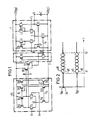
- a circuit node 2 is connected to a terminal 3 via two parallel circuit branches, one of which contains the series circuit of a load element L1 and an n-channel field effect transistor T1 and the other the series circuit of a load element L2 and an n-channel field effect transistor T2 , which is connected to a supply voltage V DD .
- the circuit node 2 is connected via a further circuit branch, which contains an n-channel field effect transistor T3 connected as a current source, to a connection 4, which is at reference potential V SS .
- the load elements L1 and L2 each consist of a p-channel field effect transistor, the drain connection of which is connected to its gate connection.
- connections 3 and 4 Between the connections 3 and 4 is the series connection of a p-channel field effect transistor T4 and an n-channel field effect transistor T5, the gate of T4 being connected to the gate of the field effect transistor forming the load element L2.
- Another circuit branch connecting terminals 3 and 4 contains the series connection of a p-channel field effect transistor T6 and an n-channel field effect transistor T7, the gate of T6 being connected to the gate of the field effect transistor forming the load element L1.
- the gate of T7 is connected to both the drain connection of T7 and the gate of T5.
- the connection point of T4 and T5 is led to the output A of the differential amplifier, while the gate connections 5 and 6 of the transistors T2 and T1 each represent the positive and the negative amplifier input.
- T 7 denotes a circuit stage for setting the quiescent currents, that is to say the currents which flow in the parallel circuit branches L1, T1 and L2, T2 without the occurrence of an input signal to be amplified at the inputs 5 and 6. It consists of the series connection of a p-channel field effect transistor T8 and an n-channel field effect transistor T9, which is connected between terminals 3 and 4. The gate of T8 lies at the connection 4 connected to V SS , so that a constant current determined by V DD and V SS flows into the series connection T8, T9. The gate of T9 is connected to the drain of T9, where T9 represents the output resistance of circuit stage 7.
- the constant current flowing through T9 causes a constant bias voltage to drop at the drain terminal of T9, which is also fed to the gate of T3 via a line 8 connecting the gates of T9 and T3 and sets this transistor to a fixed operating point, in which it has a quiescent current I O delivers.
- I O corresponds to the sum of the quiescent currents I O / 2 of the same size which flow through the parallel circuit branches L1, T1 and L2, T2.
- the gates of T1 and T2 are connected to a bias voltage U G1 , which is dimensioned such that T1 and T2 are in the conductive state. If the structural designs of the transistors L2 and T4 match, they form a current mirror which causes not only L2 but also the transistor T4 to flow through I O / 2.
- This quiescent current operation corresponds to a relatively low power consumption. Only when an input signal to be amplified occurs at amplifier inputs 5 and 6 is the modulation of transistor T3 increased so much that the difference Limit amplifier 1 is able to supply an undistorted and undelayed output signal to the load circuit connected to A, which may have a large resistance.
- a level-converting circuit PU and two p-channel field effect transistors T10 and T11 connected downstream thereof are provided, the source connections of which are each connected to connection 3, while their drain connections are connected to the drain connection of T9.
- Each of the transistors T10 and T11 is thus connected in series with the output-side resistance of circuit stage 7, each of these series circuits connecting terminals 3 and 4 to one another.
- the inputs of PU are designated 8 and 9, 8 being connected to the input 5 of the differential amplifier 1 and 9 to the input 6 of the same.
- the upper output 10 of PU is at the gate of T10, the lower output 11 at the gate of T11.
- u10 corresponds to a bias voltage value U A1 supplied to the gate of T10, on which the input signal ul amplified in PU is superimposed, while u11 is composed of the bias voltage value U A1 and an input signal u1 superimposed, amplified and inverted.
- U A1 is slightly above the threshold voltage U t of transistors T10 and T11, as is indicated in FIG. 2, each part of the negative sine half-waves of ull below U t switches transistor T11 into the conductive state, so that a first additional current of 3 flows via T11 and T9 to 4. This increases the voltage at terminal 12, which is fed to the gate of T3 is, so that the current supplied by T3 to branches L1, T1 and L2, T2 is greatly increased.
- each part of the sine half-waves of u10 which falls below U t switches transistor T10 into the conductive state, so that a second additional current flows from 3 via T10 and T9 to 4.
- the current controlled via t3 is greatly increased by the parallel circuit branches L1, T1 and L2, T2, so that good driver properties of the differential amplifier are achieved.
- the resulting higher power consumption of the amplifier is limited to the period in which the input signal u1 is present.
- the signal transmission to the output takes place in such a way that for each size difference of the currents flowing through L2 and L1 caused by the control of T2 and T1 with the input signal u1, there is a corresponding size difference of the currents through T4 and T5, which increases leads to an output current that can be tapped at A.
- the output signal responds very quickly to the fluctuations in the input signal, so that input signals with steeply rising and falling edges, for example square-wave voltages, are transmitted largely without distortion and with a large current increase to output A.
- the circuit constructed as a differential amplifier stage contains in particular two parallel current branches arranged between a circuit node 13 and the connection 3 connected to V DD , the first of which a p-channel field-effect transistor T12 in series with an n-channel field-effect transistor T13 and the second one Has p-channel field effect transistor T14 in series with an n-channel field effect transistor T15.
- the circuit node 13 is connected via a circuit branch, which contains the source-drain path of an n-channel field effect transistor T16, to the terminal 4, which is connected to the reference potential V SS .
- Input 8 corresponds to the gate connection of T15
- input 9 corresponds to the gate connection of T13
- Output 10 is connected to the connection point of transistors T14 and T15
- output 11 is connected to the connection point of transistors T12 and T13.
- To set the gate voltage of T16 a circuit branch lying between the connections 3 and 4 is used, which contains the series connection of a p-channel field effect transistor T17 and an n-channel field effect transistor T18.
- the gate of T17 is connected to terminal 4, so that a certain current flows through this series circuit, which is given by the reference potential V SS at the gate of T17.
- T18 has its gate connected to its drain. The voltage drop across this is fed via a line 14 to the gate of T16.
- a second circuit branch between 3 and 4 which contains the series circuit of a p-channel field effect transistor T19 and an n-channel field effect transistor T20, is used to set the gate voltages of T12 and T14.
- T19 is connected as a load element because its gate connection is connected to its drain connection. The voltage drop across the drain of T19 is supplied to the transistors T12 and T14 via a line 15 as a gate voltage.
- the structural dimensions of the transistors T12 and T14 must be identical to one another and different from the structural ones Distinct dimensions of the transistor T16 so far that T12 and T14 operate in the triode region, ie in the rising part of their I D / U DS characteristic, while T16 is operated in saturation. This condition can be met by making the sum of the saturation currents of T12 and T14 larger than the saturation current of T16.
- the structural dimensions of T12 and T14 are further selected so that the signal U A1 occurs at the outputs 10 and 11 without supplying an input signal u1.
- the level U A1 can also be selected so that it corresponds exactly to the value of U t or falls slightly below it.
- U A1 and U G1 are then to be interchanged, which in FIG. 2 means that the voltage profiles u5 and u6 take the place of the voltage profiles u10 and u11 and vice versa.
- PU converts a higher input level U G1 , ie the direct current component of the input signal u1, to a low output level U A1 .
- U A1 is then preferably slightly below the value of the threshold voltage U t of transistors T10 and T11, which here belong to the n-channel type.
- the value of the output level U A1 can also be selected so that it corresponds exactly to the threshold voltage U t of T10 and T11 or slightly exceeds it.
Landscapes
- Engineering & Computer Science (AREA)
- Power Engineering (AREA)
- Amplifiers (AREA)
Applications Claiming Priority (2)
| Application Number | Priority Date | Filing Date | Title |
|---|---|---|---|
| DE3824832 | 1988-07-21 | ||
| DE3824832 | 1988-07-21 |
Publications (2)
| Publication Number | Publication Date |
|---|---|
| EP0351709A2 true EP0351709A2 (fr) | 1990-01-24 |
| EP0351709A3 EP0351709A3 (fr) | 1990-11-14 |
Family
ID=6359259
Family Applications (1)
| Application Number | Title | Priority Date | Filing Date |
|---|---|---|---|
| EP19890112775 Withdrawn EP0351709A3 (fr) | 1988-07-21 | 1989-07-12 | Amplificateur différentiel à consommation de puissance réglable extérieurement |
Country Status (3)
| Country | Link |
|---|---|
| US (1) | US4956613A (fr) |
| EP (1) | EP0351709A3 (fr) |
| JP (1) | JPH0269006A (fr) |
Families Citing this family (2)
| Publication number | Priority date | Publication date | Assignee | Title |
|---|---|---|---|---|
| US5451898A (en) * | 1993-11-12 | 1995-09-19 | Rambus, Inc. | Bias circuit and differential amplifier having stabilized output swing |
| US7265620B2 (en) * | 2005-07-06 | 2007-09-04 | Pericom Semiconductor Corp. | Wide-band high-gain limiting amplifier with parallel resistor-transistor source loads |
Family Cites Families (4)
| Publication number | Priority date | Publication date | Assignee | Title |
|---|---|---|---|---|
| GB1517163A (en) * | 1975-09-18 | 1978-07-12 | Post Office | Class a amplifier |
| NL8402541A (nl) * | 1984-08-20 | 1986-03-17 | Philips Nv | Versterkerschakeling. |
| DE3701791A1 (de) * | 1987-01-22 | 1988-08-04 | Siemens Ag | Differenzverstaerker mit steuerbarer leistungsaufnahme |
| US4780688A (en) * | 1987-05-07 | 1988-10-25 | Harris Corporation | Large signal output current enhancement for a differential pair |
-
1989
- 1989-06-16 US US07/367,268 patent/US4956613A/en not_active Expired - Fee Related
- 1989-07-12 EP EP19890112775 patent/EP0351709A3/fr not_active Withdrawn
- 1989-07-17 JP JP1182764A patent/JPH0269006A/ja active Pending
Also Published As
| Publication number | Publication date |
|---|---|
| EP0351709A3 (fr) | 1990-11-14 |
| JPH0269006A (ja) | 1990-03-08 |
| US4956613A (en) | 1990-09-11 |
Similar Documents
| Publication | Publication Date | Title |
|---|---|---|
| DE69011756T2 (de) | Stromspiegelschaltung. | |
| DE69524265T2 (de) | Spannungspegelverschieber | |
| DE2811074C2 (de) | Komplementäre, leistungslose Komparator/Inverter-Schaltung | |
| EP0275940B1 (fr) | Amplificateur différentiel avec consommation de puissance pouvant être commandée | |
| DE69411217T2 (de) | Verzögerungsschaltung zum Verzögern von differentiellen Signalen | |
| DE2641860A1 (de) | Integrierte stromversorgungsschaltung | |
| DE69219182T2 (de) | Transkonduktanzoperationsverstärker mit grossem Gleichtaktpegel | |
| DE69602440T2 (de) | Niedrigspannungs-operationsverstärker mit einem der speisespannung entsprechenden spannungsbereich | |
| DE68921136T2 (de) | Transistorverstärker für hohe Anstiegsgeschwindigkeiten und kapazitive Belastungen. | |
| DE69403832T2 (de) | Integrierte Schaltung mit einem Kaskadestromspiegel | |
| DE2554054A1 (de) | Differentialverstaerkerschaltung in cmos-bauweise | |
| EP0351708A2 (fr) | Amplificateur différentiel à consommation de puissance réglable extérieurement | |
| DE10341320B4 (de) | Differenzverstärkerschaltung | |
| EP0389654B1 (fr) | Circuit amplificateur intégré | |
| DE69413235T2 (de) | In verschiedene Konfigurationen umschaltbarer Operationsverstärker | |
| DE69918394T2 (de) | Begrenzungsschaltung für einen analogen Verstärker | |
| DE69412008T2 (de) | Operationsverstärker und Verfahren dazu | |
| DE69721940T2 (de) | Pegelverschiebungsschaltung | |
| EP0544143B1 (fr) | Circuit comparateur intégré | |
| DE3021678A1 (de) | Lineare differenzverstaerkerschaltung | |
| EP0351709A2 (fr) | Amplificateur différentiel à consommation de puissance réglable extérieurement | |
| DE69522196T2 (de) | Pufferschaltung und Vorspannungsschaltung | |
| DE3721221C2 (de) | Spannungsverstärkerschaltung geringer Klirrverzerrung für widerstandsbehaftete Lasten | |
| EP0024549A1 (fr) | Convertisseur de niveau TTL pour commander des transistors à effet de champ | |
| DE69000845T2 (de) | Begrenzerschaltung mit feldeffekttransistoren. |
Legal Events
| Date | Code | Title | Description |
|---|---|---|---|
| PUAI | Public reference made under article 153(3) epc to a published international application that has entered the european phase |
Free format text: ORIGINAL CODE: 0009012 |
|
| AK | Designated contracting states |
Kind code of ref document: A2 Designated state(s): BE DE FR GB IT NL SE |
|
| PUAL | Search report despatched |
Free format text: ORIGINAL CODE: 0009013 |
|
| AK | Designated contracting states |
Kind code of ref document: A3 Designated state(s): BE DE FR GB IT NL SE |
|
| 17P | Request for examination filed |
Effective date: 19901205 |
|
| 17Q | First examination report despatched |
Effective date: 19930401 |
|
| STAA | Information on the status of an ep patent application or granted ep patent |
Free format text: STATUS: THE APPLICATION IS DEEMED TO BE WITHDRAWN |
|
| 18D | Application deemed to be withdrawn |
Effective date: 19950201 |