EP0352183A1 - Verfahren zum Montieren elektronischer Mikrokomponenten auf einer Unterlage und Zwischenprodukt - Google Patents
Verfahren zum Montieren elektronischer Mikrokomponenten auf einer Unterlage und Zwischenprodukt Download PDFInfo
- Publication number
- EP0352183A1 EP0352183A1 EP19890402041 EP89402041A EP0352183A1 EP 0352183 A1 EP0352183 A1 EP 0352183A1 EP 19890402041 EP19890402041 EP 19890402041 EP 89402041 A EP89402041 A EP 89402041A EP 0352183 A1 EP0352183 A1 EP 0352183A1
- Authority
- EP
- European Patent Office
- Prior art keywords
- micro
- component
- contacts
- sections
- support
- Prior art date
- Legal status (The legal status is an assumption and is not a legal conclusion. Google has not performed a legal analysis and makes no representation as to the accuracy of the status listed.)
- Granted
Links
Images


Classifications
-
- H—ELECTRICITY
- H05—ELECTRIC TECHNIQUES NOT OTHERWISE PROVIDED FOR
- H05K—PRINTED CIRCUITS; CASINGS OR CONSTRUCTIONAL DETAILS OF ELECTRIC APPARATUS; MANUFACTURE OF ASSEMBLAGES OF ELECTRICAL COMPONENTS
- H05K1/00—Printed circuits
- H05K1/02—Details
- H05K1/0201—Thermal arrangements, e.g. for cooling, heating or preventing overheating
- H05K1/0203—Cooling of mounted components
- H05K1/0207—Cooling of mounted components using internal conductor planes parallel to the surface for thermal conduction, e.g. power planes
-
- H—ELECTRICITY
- H05—ELECTRIC TECHNIQUES NOT OTHERWISE PROVIDED FOR
- H05K—PRINTED CIRCUITS; CASINGS OR CONSTRUCTIONAL DETAILS OF ELECTRIC APPARATUS; MANUFACTURE OF ASSEMBLAGES OF ELECTRICAL COMPONENTS
- H05K3/00—Apparatus or processes for manufacturing printed circuits
- H05K3/30—Assembling printed circuits with electric components, e.g. with resistors
- H05K3/303—Assembling printed circuits with electric components, e.g. with resistors with surface mounted components
-
- H—ELECTRICITY
- H05—ELECTRIC TECHNIQUES NOT OTHERWISE PROVIDED FOR
- H05K—PRINTED CIRCUITS; CASINGS OR CONSTRUCTIONAL DETAILS OF ELECTRIC APPARATUS; MANUFACTURE OF ASSEMBLAGES OF ELECTRICAL COMPONENTS
- H05K3/00—Apparatus or processes for manufacturing printed circuits
- H05K3/30—Assembling printed circuits with electric components, e.g. with resistors
- H05K3/32—Assembling printed circuits with electric components, e.g. with resistors electrically connecting electric components or wires to printed circuits
- H05K3/34—Assembling printed circuits with electric components, e.g. with resistors electrically connecting electric components or wires to printed circuits by soldering
- H05K3/341—Surface mounted components
- H05K3/3421—Leaded components
- H05K3/3426—Leaded components characterised by the leads
-
- H—ELECTRICITY
- H10—SEMICONDUCTOR DEVICES; ELECTRIC SOLID-STATE DEVICES NOT OTHERWISE PROVIDED FOR
- H10W—GENERIC PACKAGES, INTERCONNECTIONS, CONNECTORS OR OTHER CONSTRUCTIONAL DETAILS OF DEVICES COVERED BY CLASS H10
- H10W70/00—Package substrates; Interposers; Redistribution layers [RDL]
- H10W70/60—Insulating or insulated package substrates; Interposers; Redistribution layers
- H10W70/62—Insulating or insulated package substrates; Interposers; Redistribution layers characterised by their interconnections
- H10W70/65—Shapes or dispositions of interconnections
- H10W70/657—Shapes or dispositions of interconnections on sidewalls or bottom surfaces of the package substrates, interposers or redistribution layers
-
- H—ELECTRICITY
- H05—ELECTRIC TECHNIQUES NOT OTHERWISE PROVIDED FOR
- H05K—PRINTED CIRCUITS; CASINGS OR CONSTRUCTIONAL DETAILS OF ELECTRIC APPARATUS; MANUFACTURE OF ASSEMBLAGES OF ELECTRICAL COMPONENTS
- H05K1/00—Printed circuits
- H05K1/02—Details
- H05K1/0201—Thermal arrangements, e.g. for cooling, heating or preventing overheating
- H05K1/0203—Cooling of mounted components
- H05K1/0204—Cooling of mounted components using means for thermal conduction connection in the thickness direction of the substrate
- H05K1/0206—Cooling of mounted components using means for thermal conduction connection in the thickness direction of the substrate by printed thermal vias
-
- H—ELECTRICITY
- H05—ELECTRIC TECHNIQUES NOT OTHERWISE PROVIDED FOR
- H05K—PRINTED CIRCUITS; CASINGS OR CONSTRUCTIONAL DETAILS OF ELECTRIC APPARATUS; MANUFACTURE OF ASSEMBLAGES OF ELECTRICAL COMPONENTS
- H05K2201/00—Indexing scheme relating to printed circuits covered by H05K1/00
- H05K2201/06—Thermal details
- H05K2201/068—Thermal details wherein the coefficient of thermal expansion is important
-
- H—ELECTRICITY
- H05—ELECTRIC TECHNIQUES NOT OTHERWISE PROVIDED FOR
- H05K—PRINTED CIRCUITS; CASINGS OR CONSTRUCTIONAL DETAILS OF ELECTRIC APPARATUS; MANUFACTURE OF ASSEMBLAGES OF ELECTRICAL COMPONENTS
- H05K2201/00—Indexing scheme relating to printed circuits covered by H05K1/00
- H05K2201/10—Details of components or other objects attached to or integrated in a printed circuit board
- H05K2201/10613—Details of electrical connections of non-printed components, e.g. special leads
- H05K2201/10621—Components characterised by their electrical contacts
- H05K2201/10727—Leadless chip carrier [LCC], e.g. chip-modules for cards
-
- H—ELECTRICITY
- H05—ELECTRIC TECHNIQUES NOT OTHERWISE PROVIDED FOR
- H05K—PRINTED CIRCUITS; CASINGS OR CONSTRUCTIONAL DETAILS OF ELECTRIC APPARATUS; MANUFACTURE OF ASSEMBLAGES OF ELECTRICAL COMPONENTS
- H05K2201/00—Indexing scheme relating to printed circuits covered by H05K1/00
- H05K2201/10—Details of components or other objects attached to or integrated in a printed circuit board
- H05K2201/10613—Details of electrical connections of non-printed components, e.g. special leads
- H05K2201/10742—Details of leads
- H05K2201/10886—Other details
- H05K2201/10924—Leads formed from a punched metal foil
-
- H—ELECTRICITY
- H05—ELECTRIC TECHNIQUES NOT OTHERWISE PROVIDED FOR
- H05K—PRINTED CIRCUITS; CASINGS OR CONSTRUCTIONAL DETAILS OF ELECTRIC APPARATUS; MANUFACTURE OF ASSEMBLAGES OF ELECTRICAL COMPONENTS
- H05K2201/00—Indexing scheme relating to printed circuits covered by H05K1/00
- H05K2201/10—Details of components or other objects attached to or integrated in a printed circuit board
- H05K2201/10613—Details of electrical connections of non-printed components, e.g. special leads
- H05K2201/10742—Details of leads
- H05K2201/10886—Other details
- H05K2201/10946—Leads attached onto leadless component after manufacturing the component
-
- H—ELECTRICITY
- H05—ELECTRIC TECHNIQUES NOT OTHERWISE PROVIDED FOR
- H05K—PRINTED CIRCUITS; CASINGS OR CONSTRUCTIONAL DETAILS OF ELECTRIC APPARATUS; MANUFACTURE OF ASSEMBLAGES OF ELECTRICAL COMPONENTS
- H05K2201/00—Indexing scheme relating to printed circuits covered by H05K1/00
- H05K2201/20—Details of printed circuits not provided for in H05K2201/01 - H05K2201/10
- H05K2201/2036—Permanent spacer or stand-off in a printed circuit or printed circuit assembly
-
- H—ELECTRICITY
- H05—ELECTRIC TECHNIQUES NOT OTHERWISE PROVIDED FOR
- H05K—PRINTED CIRCUITS; CASINGS OR CONSTRUCTIONAL DETAILS OF ELECTRIC APPARATUS; MANUFACTURE OF ASSEMBLAGES OF ELECTRICAL COMPONENTS
- H05K3/00—Apparatus or processes for manufacturing printed circuits
- H05K3/30—Assembling printed circuits with electric components, e.g. with resistors
- H05K3/32—Assembling printed circuits with electric components, e.g. with resistors electrically connecting electric components or wires to printed circuits
- H05K3/34—Assembling printed circuits with electric components, e.g. with resistors electrically connecting electric components or wires to printed circuits by soldering
- H05K3/341—Surface mounted components
- H05K3/3421—Leaded components
-
- H—ELECTRICITY
- H10—SEMICONDUCTOR DEVICES; ELECTRIC SOLID-STATE DEVICES NOT OTHERWISE PROVIDED FOR
- H10W—GENERIC PACKAGES, INTERCONNECTIONS, CONNECTORS OR OTHER CONSTRUCTIONAL DETAILS OF DEVICES COVERED BY CLASS H10
- H10W70/00—Package substrates; Interposers; Redistribution layers [RDL]
- H10W70/60—Insulating or insulated package substrates; Interposers; Redistribution layers
- H10W70/67—Insulating or insulated package substrates; Interposers; Redistribution layers characterised by their insulating layers or insulating parts
- H10W70/68—Shapes or dispositions thereof
- H10W70/682—Shapes or dispositions thereof comprising holes having chips therein
-
- H—ELECTRICITY
- H10—SEMICONDUCTOR DEVICES; ELECTRIC SOLID-STATE DEVICES NOT OTHERWISE PROVIDED FOR
- H10W—GENERIC PACKAGES, INTERCONNECTIONS, CONNECTORS OR OTHER CONSTRUCTIONAL DETAILS OF DEVICES COVERED BY CLASS H10
- H10W72/00—Interconnections or connectors in packages
- H10W72/50—Bond wires
- H10W72/531—Shapes of wire connectors
- H10W72/5363—Shapes of wire connectors the connected ends being wedge-shaped
-
- H—ELECTRICITY
- H10—SEMICONDUCTOR DEVICES; ELECTRIC SOLID-STATE DEVICES NOT OTHERWISE PROVIDED FOR
- H10W—GENERIC PACKAGES, INTERCONNECTIONS, CONNECTORS OR OTHER CONSTRUCTIONAL DETAILS OF DEVICES COVERED BY CLASS H10
- H10W72/00—Interconnections or connectors in packages
- H10W72/50—Bond wires
- H10W72/551—Materials of bond wires
- H10W72/552—Materials of bond wires comprising metals or metalloids, e.g. silver
- H10W72/5525—Materials of bond wires comprising metals or metalloids, e.g. silver comprising copper [Cu]
-
- H—ELECTRICITY
- H10—SEMICONDUCTOR DEVICES; ELECTRIC SOLID-STATE DEVICES NOT OTHERWISE PROVIDED FOR
- H10W—GENERIC PACKAGES, INTERCONNECTIONS, CONNECTORS OR OTHER CONSTRUCTIONAL DETAILS OF DEVICES COVERED BY CLASS H10
- H10W90/00—Package configurations
- H10W90/701—Package configurations characterised by the relative positions of pads or connectors relative to package parts
- H10W90/751—Package configurations characterised by the relative positions of pads or connectors relative to package parts of bond wires
- H10W90/754—Package configurations characterised by the relative positions of pads or connectors relative to package parts of bond wires between a chip and a stacked insulating package substrate, interposer or RDL
-
- Y—GENERAL TAGGING OF NEW TECHNOLOGICAL DEVELOPMENTS; GENERAL TAGGING OF CROSS-SECTIONAL TECHNOLOGIES SPANNING OVER SEVERAL SECTIONS OF THE IPC; TECHNICAL SUBJECTS COVERED BY FORMER USPC CROSS-REFERENCE ART COLLECTIONS [XRACs] AND DIGESTS
- Y02—TECHNOLOGIES OR APPLICATIONS FOR MITIGATION OR ADAPTATION AGAINST CLIMATE CHANGE
- Y02P—CLIMATE CHANGE MITIGATION TECHNOLOGIES IN THE PRODUCTION OR PROCESSING OF GOODS
- Y02P70/00—Climate change mitigation technologies in the production process for final industrial or consumer products
- Y02P70/50—Manufacturing or production processes characterised by the final manufactured product
-
- Y—GENERAL TAGGING OF NEW TECHNOLOGICAL DEVELOPMENTS; GENERAL TAGGING OF CROSS-SECTIONAL TECHNOLOGIES SPANNING OVER SEVERAL SECTIONS OF THE IPC; TECHNICAL SUBJECTS COVERED BY FORMER USPC CROSS-REFERENCE ART COLLECTIONS [XRACs] AND DIGESTS
- Y10—TECHNICAL SUBJECTS COVERED BY FORMER USPC
- Y10T—TECHNICAL SUBJECTS COVERED BY FORMER US CLASSIFICATION
- Y10T29/00—Metal working
- Y10T29/49—Method of mechanical manufacture
- Y10T29/49002—Electrical device making
- Y10T29/49117—Conductor or circuit manufacturing
- Y10T29/49124—On flat or curved insulated base, e.g., printed circuit, etc.
- Y10T29/4913—Assembling to base an electrical component, e.g., capacitor, etc.
- Y10T29/49144—Assembling to base an electrical component, e.g., capacitor, etc. by metal fusion
-
- Y—GENERAL TAGGING OF NEW TECHNOLOGICAL DEVELOPMENTS; GENERAL TAGGING OF CROSS-SECTIONAL TECHNOLOGIES SPANNING OVER SEVERAL SECTIONS OF THE IPC; TECHNICAL SUBJECTS COVERED BY FORMER USPC CROSS-REFERENCE ART COLLECTIONS [XRACs] AND DIGESTS
- Y10—TECHNICAL SUBJECTS COVERED BY FORMER USPC
- Y10T—TECHNICAL SUBJECTS COVERED BY FORMER US CLASSIFICATION
- Y10T29/00—Metal working
- Y10T29/49—Method of mechanical manufacture
- Y10T29/49002—Electrical device making
- Y10T29/49117—Conductor or circuit manufacturing
- Y10T29/49124—On flat or curved insulated base, e.g., printed circuit, etc.
- Y10T29/49147—Assembling terminal to base
- Y10T29/49149—Assembling terminal to base by metal fusion bonding
Definitions
- the present invention relates to a method for mounting, on a printed circuit support, electronic micro-components to be fixed flat and provided, on their underside, with solderable contacts and for connecting them to the printed circuit, as well as a intermediate product achievable by this process.
- the invention makes it possible in particular to fix, on the support, a micro-component having a coefficient of thermal expansion markedly different from that of the support, even if it has large dimensions.
- a particularly important, although not exclusive, application of the method consists of the assembly of micro-components called “chip carriers” or “chip carriers”, lacking a fixing lug and whose size is much smaller than that of the housings. of conventional integrated circuit. It is however also applicable to other micro-components whose material is ill-suited, from the point of view of thermal expansion, to the support intended to receive them. This is the case, for example, of various passive circuits (resistance networks in particular) to be fixed on ceramic substrate or printed circuits and provided at their periphery with metallized connection notches.
- the chip holders have a ceramic base provided on its underside with contacts allowing it to be fixed flat on a support.
- the difference between the expansion coefficients of the ceramic and of the glass-epoxy or glass-polyimide laminate which constitutes most of the usual printed circuit supports leads to assemblies which cannot withstand thermal cycling.
- the constraints due to differential expansions risk destroying the contacts.
- Various palliative measures have been proposed to solve this problem.
- chip carriers have been provided with connecting tabs having a shape called "seagull wing" so that they tolerate differential expansions between base and support. The flexibility of these tabs is limited and there are only a few dimensions of chip holders provided with such tabs.
- Document FR-A-2 523 3 7 describes a method making it possible to solve the problem of differential thermal expansions in the case where the support carries welding pads between which the equipotential connections are made by sections of insulated flexible wire and not by printed tracks.
- the component is fixed flat to the support by mechanical connection means capable of tolerating differential expansion, constituted by an interlayer made of a material thermally compatible with the micro-component and electrical connections are made by welding the contacts of the micro-component on a conductive network provided on the interlayer and extending beyond the component.
- This method is however especially applicable to the production of circuits to be produced in small numbers, because of the number of connections to be created manually.
- the present invention aims in particular to allow the mounting of micro-components to be fixed flat on any type of support, such as a conventional printed circuit board (possibly multi-layer) or a thick layer or thin layer circuit board. It also aims to provide a process not only applicable to conventional chip holders having up to 84 outputs distributed with a pitch of 1.27 mm, but also extrapolable to chip holders having up to 228 output contacts and to those whose the output contacts are distributed in steps of 0.635 mm, still not very common.
- the invention notably proposes a method according to claim 1.
- the mechanical connection means are advantageously constituted by a shim with plan dimensions smaller than those of the component to release the weldable contacts, made of a material having a coefficient of expansion comparable to that of the micro-component.
- This material placed at the right of the cavity of the chip holder which receives the active component, must have an interface as conductive of heat as possible with the chip holder and with the support and it allows to evacuate the heat released by the active component.
- the wedge has a sufficient height so that the sections of flexible wires have a curvature such that the differential expansion of the support and of the component simply causes a modification of this curvature, without tensioning the sections of son: a thickness of wedge between 0 , 3 and 0.5 mm generally give satisfactory results.
- the flexible wire sections are made individually of tinned copper wire, or enameled when wire sections must cross. These sections are first fixed on the chip holder. The wedge is glued to the chip holder. Finally the sections of wire are brazed on the support in automatic or manual mode. We can in particular perform this operation using the means described in documents FR-A-2 191 399, 2 327 019 and 2 327 025 of the applicant company.
- all the sections of connecting wire to be fixed on the same micro-component are integral with an edge strip and a central zone to form a grid and are fixed in a single operation on all of the micro-component contacts.
- the edge strip and the central area are then cut and removed when they are no longer needed.
- the invention also provides an intermediate product comprising an electronic micro-component to be fixed flat and provided, on its underside, with contacts, a grid having an edge strip connecting the external ends of connecting sections welded to the contacts and a shim. of material having a coefficient of expansion compatible with that of the micro-component, of plan dimensions smaller than those of the micro-component and bonded under the micro-component.
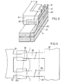
- the product shown diagrammatically in FIG. 1 comprises a printed circuit support 10 which, in the embodiment shown, has metallized intermediate planes 11 of mass and of thermal discharge, for example made of copper.
- the support 10 carries micro-components which can be of various natures. Only a chip holder 12 is shown containing an integrated circuit 14.
- the chip holder consists of a base 16 made of ceramic material, closed by a cover 18.
- the integrated circuit chip 14 is connected to the weldable contacts 20 of the chip holder in any way, for example by links 21 which are not directly concerned with the invention.
- the chip holder is equipped with sections 22 a flexible connecting wire which will generally be tinned copper wire of small diameter (0.14 mm for example).
- Each of the wire sections 22 connects one of the contacts 20 of the chip holder to a patch 13 of the printed circuit support.
- a wedge 24 in material having a coefficient of thermal expansion comparable to that of the base 16 is interposed between the support and the base.
- This wedge can in particular be made of alumina or beryllium oxide.
- the thickness of the shim will generally be between 0.3 and 0.5 mm.
- the dimensions in plan of the shim 24 are smaller than those of the base, so that the shim remains separated from the weldable contacts 20. It is consequently possible to constitute it in a product which is an electrical conductor, in the measure or the support has no metal track below.
- the wedge 24 is fixed to the base by gluing, for example using an adhesive film 26 of the type designated by the mark "Ablestick".
- the wedge 24 is fixed on the support 10 using a varnish 28, generally a polyurethane varnish, deposited at least on the central part of the wedge, that is to say where flow the heat flow due to the heating of the chip and where the interface must have as low a thermal impedance as possible.
- the heat is dissipated towards the ground planes 11 by the metal coating or occupying the holes 30 passing through the support 10 and in contact with them.
- the heat transfer is thus ensured in good conditions, the bottom of the base being pressed against the shim, itself in good thermal contact with the metallization of the holes.
- the method can be implemented by the steps successive successive.
- the base of the chip holder 16 is firstly fitted with sections 22 of tinned flexible wire.
- an apparatus of the kind shown in FIG. 2 can be used.
- the base 12 is pressed, for example by suction, on a rotary plate 32 carried by a table 34 with crossed movements and step by step advance.
- the means of connection of the plate 32 to the table 34 are provided to enable the plate to be given 90 ° orientations from one another.
- the apparatus also includes means for delivering the necessary enameled wire 36. These means may in particular comprise a spool of wire 38, rollers 40 provided with a motor for advancing the wire, each of a predetermined length, and a guide capillary 44.
- the apparatus also comprises a bracket 46 tilting in in the vertical direction and equipped with an electric welding torch 46.
- the table 34 is controlled to place the first contact 20 under the torch 46, then the welds can be performed automatically.
- the base is then taken up with a suction nozzle, making it possible not to touch the sections of wire.
- the next step is to equip the base 16 with its wedge 24.
- the base 16 is placed on the wedge, provided with an adhesive film, in a heating press which initiates the polymerization process of the adhesive film.
- a drop of varnish is deposited on the block, opposite the adhesive film and the assembly is placed on the printed circuit support.
- the sections of wire are aligned with the welding pads provided on the support and soldering is carried out individually with an apparatus which can be of one of the types described in the documents FR mentioned above. Brazing on the support does not remake the soldering already carried out on the base.
- a defective micro-component can be removed: a section of wire can be torn off, leaving a groove in which another wire can later be replaced. Varnishes are known whose shear strength is sufficiently low for the chip holder to be removed by simple twisting.
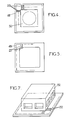
- the sections of connecting wire 22 to be fixed on the same micro-component are initially secured to an edge strip 48 and to a central zone 50 (FIG. 4) , so that the assembly constitutes a grid cut from a thin sheet (100) m for example).
- An opening is provided in the central zone 50 to allow the micro-component to be gripped directly using a suction nozzle and possibly reload the micro-component in solder which is then distributed by centrifugation.
- the sections have a main part 22a having the desired width for making the sections of connecting wire and a narrowed part 22b which is intended to be cut after welding of the sections 22 on the contacts 20.
- the parts 22a and 22b may in particular have widths 200) and 100) respectively.
- the grid is placed on the base 16, the contacts 20 of which have been pre-tinned, for example by depositing molten tin and then centrifuging. After checking the correct positioning of the grid, the sections 22 are welded at the same time using a heating electrode 52 of suitable shape (FIG. 7).
- the central area 50 is separated, for example by cutting with a knife coming to rest on the narrow parts 22b, along the line 54 of the 1 Figure 6. A reduced knife pressure is sufficient, due to the small thickness of the sections 22 and the small width of the parts 22b.
- the equipped base has the appearance shown in FIG. 5. It constitutes an intermediate product which can be sold and kept in this state until final assembly.
- the edge strip 48 constitutes a frame which maintains all the contacts at the same potential and avoids the risk of the appearance of high differential voltage which could damage the chip carried by the chip holder. In addition, the edge strip 48 maintains all the sections 22 at the correct spacing, in particular during handling and during the bonding of the wedge 24.
- the edge strip 48 is removed by sectioning using a knife, for example along line 56 (FIG. 6). All the contacts can still be soldered at the same time with a heating electrode of the same kind as that shown in FIG. 7. Due to the presence of the shim 24, the support of the heating electrode automatically gives the section 22 the required curvature so that it can later withstand differential expansions without being stressed.
- a micro-component fixed and connected by implementing the embodiment of Figures 3 to 7 can be removed and replaced.
- the sections 22 of the support 10 are dewelded, for example using a jet of hot gas.
- the micro-component can then be removed by fracturing the varnish by torsion, as long as a varnish resistant to shear, such as "solithane", was used.
- the remaining solder can be removed by heating and centrifugation before reloading.
- the method according to the invention makes it possible to fix micro-components flat on supports which also receive micro-components with through lugs.
- This support does not need to be made of material with a coefficient of expansion comparable to that of the ceramic constituting, for example, the chip holders.
- the support may in particular be a printed glass-epoxy composite circuit board or, especially when the final circuit is intended to be used in space, a glass-polyimide composite.
- the connections made are short, which is a favorable element in microwave.
- the supports used can be of a type making it possible to produce tracks by photolithography, which makes it possible to achieve thinner thicknesses than screen printing, the only process currently usable on ceramics.
- micro-components provided with their wedge and sections of junction wire can be fixed to the support by methods other than brazing, and in particular by gas reflow welding.
Landscapes
- Engineering & Computer Science (AREA)
- Microelectronics & Electronic Packaging (AREA)
- Manufacturing & Machinery (AREA)
- Electric Connection Of Electric Components To Printed Circuits (AREA)
Applications Claiming Priority (2)
| Application Number | Priority Date | Filing Date | Title |
|---|---|---|---|
| FR8809819A FR2634616B1 (fr) | 1988-07-20 | 1988-07-20 | Procede de montage de micro-composants electroniques sur un support et produit realisable par le procede |
| FR8809819 | 1988-07-20 |
Publications (2)
| Publication Number | Publication Date |
|---|---|
| EP0352183A1 true EP0352183A1 (de) | 1990-01-24 |
| EP0352183B1 EP0352183B1 (de) | 1993-09-01 |
Family
ID=9368600
Family Applications (1)
| Application Number | Title | Priority Date | Filing Date |
|---|---|---|---|
| EP19890402041 Expired - Lifetime EP0352183B1 (de) | 1988-07-20 | 1989-07-18 | Verfahren zum Montieren elektronischer Mikrokomponenten auf einer Unterlage und Zwischenprodukt |
Country Status (4)
| Country | Link |
|---|---|
| US (1) | US4959900A (de) |
| EP (1) | EP0352183B1 (de) |
| DE (1) | DE68908808T2 (de) |
| FR (1) | FR2634616B1 (de) |
Cited By (6)
| Publication number | Priority date | Publication date | Assignee | Title |
|---|---|---|---|---|
| US5063177A (en) * | 1990-10-04 | 1991-11-05 | Comsat | Method of packaging microwave semiconductor components and integrated circuits |
| FR2670074A1 (fr) * | 1990-12-03 | 1992-06-05 | Rheinmetall Gmbh | Connexion entre des composants smd et une carte de circuits imprimes. |
| AU625196B2 (en) * | 1988-12-24 | 1992-07-02 | Alcatel N.V. | A method and circuit board for mounting a semiconductor component |
| FR2671260A1 (fr) * | 1990-12-27 | 1992-07-03 | Telecommunications Sa | Support de circuit imprime electrique a moyens de drainage thermique. |
| FR2697125A1 (fr) * | 1992-10-20 | 1994-04-22 | Thomson Csf | Procédé de montage d'une microstructure et microstructure montée selon le procédé. |
| WO2007026152A1 (en) * | 2005-09-01 | 2007-03-08 | Palintest Limited | Electrochemical sensor |
Families Citing this family (27)
| Publication number | Priority date | Publication date | Assignee | Title |
|---|---|---|---|---|
| US5476970A (en) * | 1984-02-16 | 1995-12-19 | Velsicol Chemical Corporation | Method for preparing aryl ketones |
| US5091825A (en) * | 1988-03-29 | 1992-02-25 | Hughes Aircraft Company | Orthogonal bonding method and equipment |
| US5195021A (en) * | 1989-08-21 | 1993-03-16 | Texas Instruments Incorporated | Constraining core for surface mount technology |
| US5278727A (en) * | 1990-05-29 | 1994-01-11 | Digital Equipment Corporation | High density electrical interconnection device and method therefor |
| US5262594A (en) * | 1990-10-12 | 1993-11-16 | Compaq Computer Corporation | Multilayer rigid-flex printed circuit boards for use in infrared reflow oven and method for assembling same |
| JP2996510B2 (ja) * | 1990-11-30 | 2000-01-11 | 株式会社日立製作所 | 電子回路基板 |
| FR2674680B1 (fr) * | 1991-03-26 | 1993-12-03 | Thomson Csf | Procede de realisation de connexions coaxiales pour composant electronique, et boitier de composant comportant de telles connexions. |
| US5831836A (en) * | 1992-01-30 | 1998-11-03 | Lsi Logic | Power plane for semiconductor device |
| US5277612A (en) * | 1992-04-21 | 1994-01-11 | Chrysler Corporation | Carrier for guiding and supporting semiconductor devices |
| US5359768A (en) * | 1992-07-30 | 1994-11-01 | Intel Corporation | Method for mounting very small integrated circuit package on PCB |
| US5319521A (en) * | 1992-08-17 | 1994-06-07 | Rockwell International Corporation | Ceramic frames and capsules for Z-axis modules |
| US5280413A (en) * | 1992-09-17 | 1994-01-18 | Ceridian Corporation | Hermetically sealed circuit modules having conductive cap anchors |
| US5280409A (en) * | 1992-10-09 | 1994-01-18 | Sun Microsystems, Inc. | Heat sink and cover for tab integrated circuits |
| US5339272A (en) * | 1992-12-21 | 1994-08-16 | Intel Corporation | Precision voltage reference |
| US5465481A (en) * | 1993-10-04 | 1995-11-14 | Motorola, Inc. | Method for fabricating a semiconductor package |
| US5467251A (en) * | 1993-10-08 | 1995-11-14 | Northern Telecom Limited | Printed circuit boards and heat sink structures |
| US5784256A (en) * | 1994-09-14 | 1998-07-21 | Kabushiki Kaisha Toshiba | Portable computer having a circuit board including a heat-generating IC chip and a metal frame supporting the circuit board |
| US5581443A (en) * | 1994-09-14 | 1996-12-03 | Kabushiki Kaisha Toshiba | Structure for cooling a circuit module having a circuit board and a heat-generating IC chip mounted on the board, and portable electronic apparatus incorporating the structure |
| DE4446566A1 (de) * | 1994-12-24 | 1996-06-27 | Telefunken Microelectron | Mehrpoliges, oberflächenmontierbares, elektronisches Bauelement |
| US5646826A (en) * | 1995-01-26 | 1997-07-08 | Northern Telecom Limited | Printed circuit board and heat sink arrangement |
| US5930117A (en) * | 1996-05-07 | 1999-07-27 | Sheldahl, Inc. | Heat sink structure comprising a microarray of thermal metal heat channels or vias in a polymeric or film layer |
| KR100244580B1 (ko) * | 1997-06-24 | 2000-02-15 | 윤종용 | 금속 범프를 갖는 회로 기판의 제조 방법 및 그를 이용한 반도체 칩 패키지의 제조 방법 |
| US20020093802A1 (en) * | 2001-01-16 | 2002-07-18 | Knowles Gary R. | High-g mounting arrangement for electronic chip carrier |
| US6770822B2 (en) * | 2002-02-22 | 2004-08-03 | Bridgewave Communications, Inc. | High frequency device packages and methods |
| US7274050B2 (en) * | 2004-10-29 | 2007-09-25 | Avago Technologies General Ip (Singapore) Pte. Ltd. | Packaging and manufacturing of an integrated circuit |
| US8581113B2 (en) | 2007-12-19 | 2013-11-12 | Bridgewave Communications, Inc. | Low cost high frequency device package and methods |
| CN101826470B (zh) * | 2010-04-29 | 2011-08-10 | 南通富士通微电子股份有限公司 | 一种倒装焊高散热球型阵列封装方法 |
Citations (7)
| Publication number | Priority date | Publication date | Assignee | Title |
|---|---|---|---|---|
| FR2360174A1 (fr) * | 1976-07-30 | 1978-02-24 | Amp Inc | Boitier de circuit integre et son procede de fabrication |
| FR2479639A1 (fr) * | 1980-03-25 | 1981-10-02 | Thomson Csf | Dispositif d'assemblage entre composants electroniques de caracteristiques mecaniques differentes et son procede de realisation |
| FR2523397A1 (fr) * | 1982-03-08 | 1983-09-16 | Matra | Procede de montage de composants electroniques sur un support et produit realisable par le procede |
| EP0095391A2 (de) * | 1982-05-26 | 1983-11-30 | Fujitsu Limited | Montierung von leitungslosen Chip-Trägern |
| GB2149581A (en) * | 1983-11-11 | 1985-06-12 | Plessey Co Plc | Mounted integrated circuit chip carrier |
| US4750080A (en) * | 1987-02-13 | 1988-06-07 | Cumming Corporation | Film cleaner method and apparatus |
| WO1988005428A1 (en) * | 1987-01-21 | 1988-07-28 | Hughes Aircraft Company | Method for connecting leadless chip packages and articles |
Family Cites Families (4)
| Publication number | Priority date | Publication date | Assignee | Title |
|---|---|---|---|---|
| US3700788A (en) * | 1971-01-28 | 1972-10-24 | Coars Porcelain Co | Electrical component package |
| US4381602A (en) * | 1980-12-29 | 1983-05-03 | Honeywell Information Systems Inc. | Method of mounting an I.C. chip on a substrate |
| US4750089A (en) * | 1985-11-22 | 1988-06-07 | Texas Instruments Incorporated | Circuit board with a chip carrier and mounting structure connected to the chip carrier |
| US4827611A (en) * | 1988-03-28 | 1989-05-09 | Control Data Corporation | Compliant S-leads for chip carriers |
-
1988
- 1988-07-20 FR FR8809819A patent/FR2634616B1/fr not_active Expired - Fee Related
-
1989
- 1989-07-17 US US07/380,433 patent/US4959900A/en not_active Expired - Fee Related
- 1989-07-18 DE DE89402041T patent/DE68908808T2/de not_active Expired - Fee Related
- 1989-07-18 EP EP19890402041 patent/EP0352183B1/de not_active Expired - Lifetime
Patent Citations (7)
| Publication number | Priority date | Publication date | Assignee | Title |
|---|---|---|---|---|
| FR2360174A1 (fr) * | 1976-07-30 | 1978-02-24 | Amp Inc | Boitier de circuit integre et son procede de fabrication |
| FR2479639A1 (fr) * | 1980-03-25 | 1981-10-02 | Thomson Csf | Dispositif d'assemblage entre composants electroniques de caracteristiques mecaniques differentes et son procede de realisation |
| FR2523397A1 (fr) * | 1982-03-08 | 1983-09-16 | Matra | Procede de montage de composants electroniques sur un support et produit realisable par le procede |
| EP0095391A2 (de) * | 1982-05-26 | 1983-11-30 | Fujitsu Limited | Montierung von leitungslosen Chip-Trägern |
| GB2149581A (en) * | 1983-11-11 | 1985-06-12 | Plessey Co Plc | Mounted integrated circuit chip carrier |
| WO1988005428A1 (en) * | 1987-01-21 | 1988-07-28 | Hughes Aircraft Company | Method for connecting leadless chip packages and articles |
| US4750080A (en) * | 1987-02-13 | 1988-06-07 | Cumming Corporation | Film cleaner method and apparatus |
Cited By (8)
| Publication number | Priority date | Publication date | Assignee | Title |
|---|---|---|---|---|
| AU625196B2 (en) * | 1988-12-24 | 1992-07-02 | Alcatel N.V. | A method and circuit board for mounting a semiconductor component |
| US5063177A (en) * | 1990-10-04 | 1991-11-05 | Comsat | Method of packaging microwave semiconductor components and integrated circuits |
| FR2670074A1 (fr) * | 1990-12-03 | 1992-06-05 | Rheinmetall Gmbh | Connexion entre des composants smd et une carte de circuits imprimes. |
| FR2671260A1 (fr) * | 1990-12-27 | 1992-07-03 | Telecommunications Sa | Support de circuit imprime electrique a moyens de drainage thermique. |
| EP0494560A3 (en) * | 1990-12-27 | 1992-08-12 | Sat (Societe Anonyme De Telecommunications) | Support for printed circuits with heat dissipation means |
| FR2697125A1 (fr) * | 1992-10-20 | 1994-04-22 | Thomson Csf | Procédé de montage d'une microstructure et microstructure montée selon le procédé. |
| WO2007026152A1 (en) * | 2005-09-01 | 2007-03-08 | Palintest Limited | Electrochemical sensor |
| US8142641B2 (en) | 2005-09-01 | 2012-03-27 | Palintest Limited | Electrochemical sensor |
Also Published As
| Publication number | Publication date |
|---|---|
| EP0352183B1 (de) | 1993-09-01 |
| FR2634616B1 (fr) | 1995-08-25 |
| DE68908808D1 (de) | 1993-10-07 |
| US4959900A (en) | 1990-10-02 |
| DE68908808T2 (de) | 1993-12-23 |
| FR2634616A1 (fr) | 1990-01-26 |
Similar Documents
| Publication | Publication Date | Title |
|---|---|---|
| EP0352183B1 (de) | Verfahren zum Montieren elektronischer Mikrokomponenten auf einer Unterlage und Zwischenprodukt | |
| CN100381025C (zh) | 多层结构的柔性布线板及其制造方法 | |
| GB2382542A (en) | Reflow soldering process for mounting electronic components onto a substrate | |
| JPH05243736A (ja) | プリント回路板の製造方法 | |
| EP0717442B1 (de) | Träger für integrierten Schaltkreis zur Kontaktierung eines anderen Trägers mittels Kontaktkugeln | |
| EP0044247B1 (de) | Verfahren zur Herstellung eines Trägers für elektronische Elemente zur Verbindung integrierter Halbleiteranordnungen | |
| EP0055640A1 (de) | Klemmanordnung für aufeinandergelegte Elemente ausgerichteter Gruppen, insbesondere für die elektrische Verbindung leitender Elemente | |
| EP0178977A1 (de) | Ein in ein Plastikgehäuse montiertes Halbleiterbauelement und Verfahren zu seiner Herstellung | |
| EP1440478A1 (de) | Anordnung von photovoltaischen zellen und herstellungsverfahren | |
| EP0903811B1 (de) | Zwischenstück für mikroelektronisches Gehäuse und Verfahren zur Herstellung eines solchen Zwischenstücks | |
| FR2739731A1 (fr) | Procede de raccordement de micro-cables coaxiaux aux pistes d'un circuit imprime | |
| FR2724051A1 (fr) | Montage de dispositif electronique et son procede de fabrication | |
| FR2663494A1 (fr) | Dispositif electronique a substrat et boitier pour plaquette a circuit imprime. | |
| FR2782440A1 (fr) | Structure de montage pour circuit integre a grande echelle | |
| EP0117804B1 (de) | Herstellungsverfahren eines Mikrowellenhohlraumresonators und nach diesem Verfahren hergestellter Hohlraumresonator | |
| FR2523397A1 (fr) | Procede de montage de composants electroniques sur un support et produit realisable par le procede | |
| FR2479639A1 (fr) | Dispositif d'assemblage entre composants electroniques de caracteristiques mecaniques differentes et son procede de realisation | |
| WO2004075304A1 (fr) | Procede de realisation d’un module photovoltaique et module photovoltaique realise par ce procede | |
| FR2571547A1 (fr) | Circuit hybride reportable sur un support comportant un reseau d'interconnexion a haute densite | |
| JPH01209736A (ja) | 半導体素子の交換方法 | |
| FR2483126A1 (fr) | Procede d'elimination des plots de soudure demeurant sur un substrat ceramique apres retrait d'une microplaquette semi-conductrice, par absorption dans un bloc de cuivre poreux et application au retravaillage des modules | |
| EP0242667B1 (de) | Lötwerkzeug für elektronische Vorrichtungen | |
| FR2697125A1 (fr) | Procédé de montage d'une microstructure et microstructure montée selon le procédé. | |
| FR2666446A1 (fr) | Procede de montage de microcomposant electronique sur un support et produit intermediaire de mise en óoeuvre du procede. | |
| EP0163581A1 (de) | Herstellungsverfahren einer elektrischen Anschlussvorrichtung zwischen zwei Leiterplatten, Vorrichtung und Verfahren zum elektrischen Anschluss unter Anwendung dieser Vorrichtung |
Legal Events
| Date | Code | Title | Description |
|---|---|---|---|
| PUAI | Public reference made under article 153(3) epc to a published international application that has entered the european phase |
Free format text: ORIGINAL CODE: 0009012 |
|
| AK | Designated contracting states |
Kind code of ref document: A1 Designated state(s): BE DE GB IT |
|
| 17P | Request for examination filed |
Effective date: 19900306 |
|
| RAP1 | Party data changed (applicant data changed or rights of an application transferred) |
Owner name: MATRA ESPACE |
|
| 17Q | First examination report despatched |
Effective date: 19911025 |
|
| RAP1 | Party data changed (applicant data changed or rights of an application transferred) |
Owner name: MATRA MARCONI SPACE FRANCE |
|
| GRAA | (expected) grant |
Free format text: ORIGINAL CODE: 0009210 |
|
| AK | Designated contracting states |
Kind code of ref document: B1 Designated state(s): BE DE GB IT |
|
| GBT | Gb: translation of ep patent filed (gb section 77(6)(a)/1977) |
Effective date: 19930831 |
|
| REF | Corresponds to: |
Ref document number: 68908808 Country of ref document: DE Date of ref document: 19931007 |
|
| ITF | It: translation for a ep patent filed | ||
| PLBE | No opposition filed within time limit |
Free format text: ORIGINAL CODE: 0009261 |
|
| STAA | Information on the status of an ep patent application or granted ep patent |
Free format text: STATUS: NO OPPOSITION FILED WITHIN TIME LIMIT |
|
| 26N | No opposition filed | ||
| PGFP | Annual fee paid to national office [announced via postgrant information from national office to epo] |
Ref country code: GB Payment date: 19990713 Year of fee payment: 11 |
|
| PGFP | Annual fee paid to national office [announced via postgrant information from national office to epo] |
Ref country code: DE Payment date: 19990715 Year of fee payment: 11 |
|
| PGFP | Annual fee paid to national office [announced via postgrant information from national office to epo] |
Ref country code: BE Payment date: 19990730 Year of fee payment: 11 |
|
| PG25 | Lapsed in a contracting state [announced via postgrant information from national office to epo] |
Ref country code: GB Free format text: LAPSE BECAUSE OF NON-PAYMENT OF DUE FEES Effective date: 20000718 |
|
| PG25 | Lapsed in a contracting state [announced via postgrant information from national office to epo] |
Ref country code: BE Free format text: LAPSE BECAUSE OF NON-PAYMENT OF DUE FEES Effective date: 20000731 |
|
| BERE | Be: lapsed |
Owner name: MATRA MARCONI SPACE FRANCE Effective date: 20000731 |
|
| GBPC | Gb: european patent ceased through non-payment of renewal fee |
Effective date: 20000718 |
|
| PG25 | Lapsed in a contracting state [announced via postgrant information from national office to epo] |
Ref country code: DE Free format text: LAPSE BECAUSE OF NON-PAYMENT OF DUE FEES Effective date: 20010501 |
|
| PG25 | Lapsed in a contracting state [announced via postgrant information from national office to epo] |
Ref country code: IT Free format text: LAPSE BECAUSE OF NON-PAYMENT OF DUE FEES;WARNING: LAPSES OF ITALIAN PATENTS WITH EFFECTIVE DATE BEFORE 2007 MAY HAVE OCCURRED AT ANY TIME BEFORE 2007. THE CORRECT EFFECTIVE DATE MAY BE DIFFERENT FROM THE ONE RECORDED. Effective date: 20050718 |