EP0352934A2 - Insertion et enlèvement d'un circuit dans un réseau à bus - Google Patents
Insertion et enlèvement d'un circuit dans un réseau à bus Download PDFInfo
- Publication number
- EP0352934A2 EP0352934A2 EP89307046A EP89307046A EP0352934A2 EP 0352934 A2 EP0352934 A2 EP 0352934A2 EP 89307046 A EP89307046 A EP 89307046A EP 89307046 A EP89307046 A EP 89307046A EP 0352934 A2 EP0352934 A2 EP 0352934A2
- Authority
- EP
- European Patent Office
- Prior art keywords
- circuit
- network
- bus
- circuit device
- output driver
- Prior art date
- Legal status (The legal status is an assumption and is not a legal conclusion. Google has not performed a legal analysis and makes no representation as to the accuracy of the status listed.)
- Withdrawn
Links
Images






Classifications
-
- G—PHYSICS
- G06—COMPUTING OR CALCULATING; COUNTING
- G06F—ELECTRIC DIGITAL DATA PROCESSING
- G06F13/00—Interconnection of, or transfer of information or other signals between, memories, input/output devices or central processing units
- G06F13/38—Information transfer, e.g. on bus
- G06F13/40—Bus structure
- G06F13/4063—Device-to-bus coupling
- G06F13/4068—Electrical coupling
- G06F13/4081—Live connection to bus, e.g. hot-plugging
Definitions
- the present invention relates to the insertion and removal of a circuit device into a bus network. It is particularly, but not exclusively, concerned with the case where that circuit device is a printed circuit board.
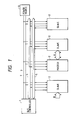
- FIG. 1 of the accompanying drawings shows a schematic block diagram of such an arrangement, which a plurality of circuit devices 2 are interconnected to a bus controller via a bus. That bus comprises an address and/or data bus (communication bus) 5, a control bus 4, and power buses 3,7 connected to a power source 6.
- One of the circuit devices 2 is a master, which controls the other circuit devices 2 which act as slaves.
- the master circuit device signals to that slave, and to the bus controller, via the control bus 4, and then data can be passed between master and slave along the address and data bus 5 as indicated by arrow A.
- the bus controller 1 ensures that the signalling is controlled in the desired way.
- US 4079440 proposes a system in which each circuit device is mounted on a printed circuit board, and the board has at least two connector plugs for connecting it to the power supply, with those plugs being of different lengths. Therefore, during insertion and removal, the time of contact with the power line of those two connector plugs is different, and this difference can be used to decrease fluctuations of the power source voltage during insertion and removal.
- this is only a limited solution to the problem, since it does not resolve all the causes of faulty signalling.
- US 4200865 discloses an arrangement in which the circuit devices are again mounted on a printed circuit board for insertion into a bus network, and the circuit board is designed so that the input to or the output from the board can be locked in response to the presence of two conditions, namely the application of a request for removal or insertion, and the fact that the circuit device is not signalling to any other device.
- the circuit components of the circuit device are connected to an address bus via an output driver, and the aim of the disclosure of US 4200865 is to lock that bus driver to prevent the bus line from being electrically disturbed.
- the present invention seeks to overcome, or at least ameliorate, the problems of the prior art by reducing or eliminating the risk of faults in signalling when a circuit device (which may be mounted on a printed circuit board) is inserted or removed into a bus network interconnecting a plurality of such devices.
- the present invention proposes that, on insertion, the first step is for the circuit device to generate a signal which prevents the other circuit devices (which are under power) from signalling on the communication bus of the bus network, and then powering the output driver of the circuit device. The signal is maintained until the output driver is stabilised, and it can then be removed. Similarly, on removal, a signal is supplied to the bus network to inhibit other circuit devices from transmitting, the power is removed from the output driver, the signal maintained until the output driver is stable, and only then is the circuit device removed. To express this in another way, the invention proposes that, on insertion or removal, the circuit device to be inserted or removed "occupies" the bus until insertion or removal is complete.
- the signalling described above will be controlled by a suitable control device in the circuit device. That control device controls the signalling to the bus network, and also controls the switching of power to the output driver in timed relationship with that signal.
- the act of physically inserting or removing the circuit device connects both the control circuit and the output driver physically to the bus network, but the device is arranged so that only the control device (and possibly other circuit components, but not including the output driver), be powered immediately on insertion. Then, the signal is generated to inhibit other devices from signalling on the communications bus, and then the output driver can be powered. Once the powering is stable, the circuit device may operate normally. On removal, the procedure is similar, with the powering of the control device remaining until the disconnection of the output driver is complete.
- the present invention has a number of aspects. It is concerned with the method and removal of a circuit device into a bus network having a plurality of powered circuit devices, to a circuit network having a plurality of such circuit devices interconnected by a bus network, to a method of maintaining such a circuit network, to the circuit device itself and to a computer system incorporating the network.
- the bus network and in particular the communication bus of that network, is not disturbed during insertion or removal of a circuit device, since the bus is effectively "occupied" by that device and other devices cannot be signalling on the bus. Occupation of the bus is released when the supply of power to the output driver is stabilised on disconnection and removal, and this enables the bus occupation time to be minimised.
- Figure 2 illustrates the connection of a circuit device to a bus network.
- the bus network shown in Figure 2 is the same as that in Figure 1, and furthermore further circuit devices 2 may also be connected to the bus network in a similar manner to that illustrated in Figure 1.
- the circuit device 2 comprises an electronic circuit 29 which contains the circuit components which define the operation to be carried out by the device 2. That electronic circuit 29 is connected via an interface circuit 28 to an output driver (bus driver) 21, which in turn is connected to the data bus (communications bus) 5. Thus, the electronic circuit 29 can signal via the interface circuit 28 and the bus driver 21 to the address bus. Similarly, signals from other circuit devices transmitted on the address bus 5 may be received via an address data receiver 26, which is connected to the interface circuit 28 and so permits those signals to be transmitted to the circuit 29.
- an output driver bus driver
- the circuit device 2 is also connected to the control bus 4 via a bus access controller 27. Connected to that access controller 27 is a active line insertion/removal controller (control device) 20 which controls the operation of the circuit device 2 in a manner which will be described.
- a bus access controller 27 Connected to that access controller 27 is a active line insertion/removal controller (control device) 20 which controls the operation of the circuit device 2 in a manner which will be described.
- the circuit device 2 is connected to the power source 6 via power buses 3 and 7, and the signal from those power buses passes via a switch 23 to the control device 20, to the interface circuit 28, and to the circuit 29.
- that switch 23 passes to the output driver 21 and to the data receiver 26, but interposed therebetween is a relay 22 controlled by the control device 20.
- a switch 24 is also connected to the control device 20, as is an LED (display) 25.
- circuit device 2 is to be removed from the bus network.
- the first stage is that switch 24 is opened, as shown in Figure 3, to generate a signal via line 16 to the control device 20.
- That control device then generates a signal via line 8 to the access controller 27, which in turn generates a signal (bus request) via line 12 to the control bus 4.
- That signal signals to the bus controller that the circuit device 2 to be removed is to "occupy" the bus, i.e. that other circuit devices connected to the bus network should not be permitted to transmit.
- the bus controller determines a time when no other circuit device is signalling, and transmits a signal (bus request grant) via the control bus 4 which is received on line 13 to the access controller 27. It is this signal that indicates that the circuit device 2 to be removed "occupies" the bus. The signal is passed via line 9 to the control device 20.
- the control device 20 On receipt of this signal, the control device 20 generates a signal on line 10 which opens the relay 22 and so cuts off the power from the output driver 21 and the data receiver 26. Effectively, line 11 is disconnected from the power supply whilst power to the other parts of the circuit device 2 remains.
- the control device 20 generate a signal (bus busy) which is fed via line 19, the access controller 27, and line 14 to the control bus 4.
- control device 20 simply to wait for a predetermined time t1, which is known to be longer than the unstable time of the output driver 21 before operating further.
- means may be provided to detect the state of the output driver 21 and signal to the control device 20 when the output driver 21 is in a stable state (at zero power on removal).
- control device 20 After the output driver 21 becomes stably off, the control device 20 removes the signal via lines 12 and 14 to the bus controller, thereby indicating that the device 2 no longer needs to occupy the data bus.
- the control device 20 generates a signal on line 17 to the LED 25, which is illuminated to show that the circuit device 2 is ready for removal.
- the switch 23 is opened to disconnect the control device 20, and the other parts of the circuit device 2 from the power supply, and then the circuit device 2 may be physically removed from the bus network.
- a signal is sent from the bus controller 1 and is received on line 13, and an appropriate signal sent via line 9 to the controller, generating a bus occupancy signal on line 19 and via the access controller 27 and line 14 to indicate to the other circuit devices that the bus network is occupied.
- the processing must then halt until the power to the output driver is stable, and again this may be for a predetermined time t1 or by some suitable detection.
- the control device 20 sends a signal via line 8, which is transmitted via the access controller 27 and line 12 to the control bus 4, and hence to the bus controller 1, to signal that the newly inserted circuit device 2 no longer needs to occupy the network.
- the signals are removed from lines 12 and 14, and the return signal from the bus controller 1 received on line 13 signals to the control device 20 to activate the LED 25.
- switch 24 is closed, and the control device 20 then cuts off the power to the LED 25. Insertion is then complete.
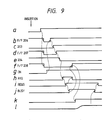
- Figs. 3 and 4 illustrate how, during the unstable period of the output driver 21 and data receiver 26, a bus occupy signal is supplied.
- Figure 7 corresponds to Figure 2, but shows the control device 20 in more detail.
- the controller 20 comprises a sequence controller 25 which determines the timing of the operation of the controller 20, three flip-flops 206, 207, 208 connected to transistor switches 200, 201, 202 and also connected via a logic gate 214 and amplifier 215 to the LED 25.
- the relay 203 is activated and the transistors 200 to 202 are all turned on. Therefore, the contact point of the relay 204 is off and the contact point of the relay 22 is on.
- a closed circuit for holding the relay 22 is formed via Vcc ⁇ coil 203A ⁇ contact point A 203B ⁇ transistor 200 even when the switch 24 is turned off, and the relay 203 maintains itself.
- the relay 203 is not excited when the power supply Vcc is interrupted or when the transistor 200 is turned off.
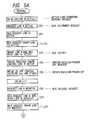
- the switch 24 is turned off, first (step (a) in Fig. 8).
- the output driver 21 When the switch 24 is turned off, the output driver 21 generates a bus occupation request REQ which is sent to the bus controller 1 via bus 5 (step (b) in Fig. 8).
- the bus controller 1 sends a bus occupation permission (REQG) to the circuit device (step (c)).
- the circuit device 2 then sends a BUS BUSY signal to the bus 4 from the gate 210A that indicates the bus occupation (step (d)).
- the circuit device 2 is allowed to occupy the bus.
- the flip-flop 208 When the bus is occupied, the flip-flop 208 produces an output Q at the L level to turn the transistor 202 off (step (e)).
- the transistor 202 that is turned off causes the contact of the relay 22 to be turned off (step (f)) and the feed of power to the bus driver 21 is interrupted.
- the output driver 21 With the feed of power being interrupted, the output driver 21 is powered down, with a slight delay in time. This is due to delay in mechanical operation of the relay 205, since it is an electromagnetic switch. The time is slightly delayed even when a transistor switch is used instead of the relay 205, and the same idea holds true.
- the output driver 21 is unstable (step (g)). After this unstable period, the gate 210A produces a BUS BUSY signal at the L level (step (h)).
- the flip-flop 207 produces an output Q at the L level to turn the transistor 201 off (step (i)). Therefore, the contact of the relay 204 is turned on to lock the driver 210 and the output of the gate 210A. Further, the flip-flop 206 produces the output Q at the L level to turn the transistor 200 off (step (j)). Accordingly, the relay 203 is not activated, and all the contacts of the relay 203 including the contact 203A are turned off (step (k)). Thus, the electric power is not fed to the relays 204, 205, nor to driver 210, or gate 210A of the access controller 27. The power feed switch 23 is then turned off. The feed of power to the circuit device 2 is now completely cut off; i.e., the circuit device 2 can be removed under the condition where the feed of power is completely stopped.
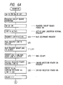
- the circuit device 2 is inserted after the switch 24 is turned off. After insertion, the power feed switch 23 is turned on (step (a)). Then, the flip-flops 206 to 208 produce outputs Q at the L level to turn the switch 209 on (step (b)). At this moment, since the flip-flop 206 produces an output Q at the L level, the transistor 200 is turned off and the relay 203 is not excited.
- the flip-flop 206 then produces an output Q at the H level, and the relay 203 is excited to turn the contact points on (step (c)). Therefore, power Vcc is fed to the relays 204, 205, driver 210 for bus control signal, and to gate 210A.
- Flip-flop 207 then produces an output Q at the H level (step (d)) to turn the transistor 201 on, to turn the contact B of the relay 204 off (step (e)), and to release the driver 210 for bus control signal and the gate 210A from the locked condition. Since the driver 210 and 210A are released from the locked condition, the circuit device 2 sends a bus occupation request REQ (step (h)) to the bus via driver 27. As for the case of removal, the circuit device 2 occupies the bus (generates BUSY signal, step (j)) under the condition where the bus is not occupied by any other circuit device.
- the flip-flop 208 produces an output Q at the H level (step (f)), whereby the transistor 202 is turned on, power is fed to the output driver 21 (step (k)), when the output driver 21 is stable (step (c)) the BUSY signal that indicates the condition of bus occupation is not produced (step (j)), and the insertion is completed.
- relays 203, 204 and 205 are used. However, it is also allowable to use electronic switches such as transistors in their place. This can be adapted to a system having a bus occupation monitoring time shorter than that of the relays.
- FIG. 10 the assembly of a plurality of output devices into a network corresponding to Figure 1, and their mounting in a computer will now be described.
- a plurality of circuit boards 300,301 are mounted in a frame 302.
- One of those circuit boards 300 may house the bus controller, and circuit board 301 illustrates a circuit board on which an output device 2 corresponding to the present invention is inserted, connected via suitable physical sockets 303,304 to the bus network shown at 4 and 5.
- the frame 302 is mounted in a housing 305, which also contains the power supply 6.
- Figure 10 also illustrates the two visible external switches 23,24 of the circuit device 2, and the LED 25. Those switches 23,24 form the user operated controls during removal and insertion as has been described above.
- circuit devices can be inserted or removed from a powered network without affecting other circuit devices connected to th at network. Maintenance of the system is rendered more simple, since a faulty board can be removed easily and a new board inserted. Poewr need not be interrupted during removal of a faulty board, so that the operation of a computer system incorporating such output devices need not be stopped, which also improves reliability.
- the circuit devices are normally mounted on a printed circuit board, for ease of handling.
Landscapes
- Engineering & Computer Science (AREA)
- General Engineering & Computer Science (AREA)
- Theoretical Computer Science (AREA)
- Computer Hardware Design (AREA)
- Physics & Mathematics (AREA)
- General Physics & Mathematics (AREA)
- Small-Scale Networks (AREA)
Applications Claiming Priority (2)
| Application Number | Priority Date | Filing Date | Title |
|---|---|---|---|
| JP171779/88 | 1988-07-12 | ||
| JP17177988 | 1988-07-12 |
Publications (2)
| Publication Number | Publication Date |
|---|---|
| EP0352934A2 true EP0352934A2 (fr) | 1990-01-31 |
| EP0352934A3 EP0352934A3 (fr) | 1990-04-25 |
Family
ID=15929524
Family Applications (1)
| Application Number | Title | Priority Date | Filing Date |
|---|---|---|---|
| EP89307046A Withdrawn EP0352934A3 (fr) | 1988-07-12 | 1989-07-11 | Insertion et enlèvement d'un circuit dans un réseau à bus |
Country Status (3)
| Country | Link |
|---|---|
| US (1) | US5247619A (fr) |
| EP (1) | EP0352934A3 (fr) |
| JP (1) | JPH02125314A (fr) |
Cited By (3)
| Publication number | Priority date | Publication date | Assignee | Title |
|---|---|---|---|---|
| FR2671887A1 (fr) * | 1991-01-21 | 1992-07-24 | Systolic Sarl | Dispositif electronique permettant la connexion et la deconnexion d'une ligne de bus d'un systeme informatique. |
| EP0548382A1 (fr) * | 1991-12-20 | 1993-06-30 | Siemens Nixdorf Informationssysteme Aktiengesellschaft | Méthode et dispositif d'échange de modules dans un système de bus en fonctionnement |
| EP0559454A1 (fr) * | 1992-03-06 | 1993-09-08 | Data General Corporation | Remplacement on-line d'un module dans un système de traitement de données à modules multiples |
Families Citing this family (25)
| Publication number | Priority date | Publication date | Assignee | Title |
|---|---|---|---|---|
| JP2752247B2 (ja) * | 1990-11-29 | 1998-05-18 | 富士通株式会社 | 情報記憶装置 |
| JPH05204785A (ja) * | 1992-01-29 | 1993-08-13 | Fujitsu Ltd | 監視バス保護方式、監視バス保護方法および監視バス保護装置 |
| US5678197A (en) * | 1993-02-26 | 1997-10-14 | Motorola, Inc. | Method for reprogramming a communication unit's access to a wireless communication system |
| JP2636141B2 (ja) * | 1993-07-09 | 1997-07-30 | 日本電気株式会社 | 活線挿抜方法 |
| US5579491A (en) * | 1994-07-07 | 1996-11-26 | Dell U.S.A., L.P. | Local proactive hot swap request/acknowledge system |
| US5555510A (en) * | 1994-08-02 | 1996-09-10 | Intel Corporation | Automatic computer card insertion and removal algorithm |
| JPH0895687A (ja) * | 1994-09-26 | 1996-04-12 | Fujitsu Ltd | I/oカード、このi/oカードに接続される接続ケーブル及びi/oカードのパワーセーブ方法 |
| US5586271A (en) * | 1994-09-27 | 1996-12-17 | Macrolink Inc. | In-line SCSI bus circuit for providing isolation and bi-directional communication between two portions of a SCSI bus |
| KR970010634B1 (ko) * | 1994-10-25 | 1997-06-28 | 삼성전자 주식회사 | 네트워크 하이버네이션 시스템 |
| US5581712A (en) * | 1994-11-17 | 1996-12-03 | Intel Corporation | Method and apparatus for managing live insertion of CPU and I/O boards into a computer system |
| JP2682503B2 (ja) * | 1995-03-24 | 1997-11-26 | 日本電気株式会社 | 活線挿抜システム |
| KR0151663B1 (ko) * | 1995-05-17 | 1998-10-15 | 김광호 | 체결상태 감지장치를 갖는 도킹 스테이션 및 휴대용 컴퓨터 동작 모드 제어방법 |
| US5740378A (en) * | 1995-08-17 | 1998-04-14 | Videoserver, Inc. | Hot swap bus architecture |
| KR0156802B1 (ko) * | 1995-11-07 | 1998-11-16 | 김광호 | 네트워크 하이버네이션 시스템 및 그 제어 방법 |
| US5974552A (en) * | 1995-12-29 | 1999-10-26 | Samsung Electronics Co., Ltd. | Method and apparatus for executing a scheduled operation after wake up from power off state |
| US5812798A (en) * | 1996-01-26 | 1998-09-22 | Motorola, Inc. | Data processing system for accessing an external device and method therefore |
| US5922060A (en) * | 1996-12-31 | 1999-07-13 | Compaq Computer Corporation | Expansion card insertion and removal |
| US5943482A (en) * | 1996-06-05 | 1999-08-24 | Compaq Computer Corporation | Expansion card insertion and removal |
| US6073196A (en) * | 1996-06-05 | 2000-06-06 | Compaq Computer Corporation | Using communication cycles for connecting and disconnecting devices in a computer system |
| US6101322A (en) * | 1996-06-05 | 2000-08-08 | Compaq Computer Corporation | Removal and insertion of expansion cards in a computer system |
| US5822196A (en) * | 1996-06-05 | 1998-10-13 | Compaq Computer Corporation | Securing a card in an electronic device |
| US6098132A (en) * | 1996-06-05 | 2000-08-01 | Compaq Computer Corporation | Installation and removal of components of a computer |
| KR100244778B1 (ko) | 1997-07-19 | 2000-02-15 | 윤종용 | 정상 동작중인 시스템에 보드를 실장 또는 탈장하는 회로 |
| US6032209A (en) * | 1998-07-24 | 2000-02-29 | Storage Technology Corporation | Hot-swappable high speed point-to-point interface |
| US6594721B1 (en) * | 2000-02-29 | 2003-07-15 | Hewlett-Packard Development Company, L.P. | Surprise hot bay swapping of IDE/ATAPI devices |
Family Cites Families (9)
| Publication number | Priority date | Publication date | Assignee | Title |
|---|---|---|---|---|
| JPS5395521A (en) * | 1977-02-02 | 1978-08-21 | Hitachi Ltd | Printed circuit board capable for live line connection and removal |
| US4562535A (en) * | 1982-04-05 | 1985-12-31 | Texas Instruments Incorporated | Self-configuring digital processor system with global system |
| US4510553A (en) * | 1983-01-24 | 1985-04-09 | Burroughs Corporation | Electromechanical assembly for aligning, discharging, and sequentially engaging conductors of a P.C. board with a backplane |
| US4635192A (en) * | 1983-12-06 | 1987-01-06 | Tri Sigma Corporation | Self configuring bus structure for computer network |
| US4704599A (en) * | 1984-06-20 | 1987-11-03 | Kimmel Arthur T | Auxiliary power connector and communication channel control circuit |
| US4609829A (en) * | 1984-08-23 | 1986-09-02 | Ncr Corporation | Apparatus for assisting in the connection and disconnection of a board with an energized circuit |
| DE3504560A1 (de) * | 1985-02-11 | 1986-08-14 | Siemens AG, 1000 Berlin und 8000 München | Anordnung zum anschluss von in baugruppentraeger einschiebbaren baugruppen |
| EP0241905A3 (fr) * | 1986-04-14 | 1990-04-25 | Siemens Nixdorf Informationssysteme Aktiengesellschaft | Plaquette de circuit pour insertion en ligne dans un système ordinateur |
| US4835737A (en) * | 1986-07-21 | 1989-05-30 | American Telephone And Telegraph Company, At&T Bell Laboratories | Method and apparatus for controlled removal and insertion of circuit modules |
-
1989
- 1989-07-05 US US07/375,826 patent/US5247619A/en not_active Expired - Fee Related
- 1989-07-11 EP EP89307046A patent/EP0352934A3/fr not_active Withdrawn
- 1989-07-12 JP JP1178114A patent/JPH02125314A/ja active Pending
Cited By (5)
| Publication number | Priority date | Publication date | Assignee | Title |
|---|---|---|---|---|
| FR2671887A1 (fr) * | 1991-01-21 | 1992-07-24 | Systolic Sarl | Dispositif electronique permettant la connexion et la deconnexion d'une ligne de bus d'un systeme informatique. |
| EP0548382A1 (fr) * | 1991-12-20 | 1993-06-30 | Siemens Nixdorf Informationssysteme Aktiengesellschaft | Méthode et dispositif d'échange de modules dans un système de bus en fonctionnement |
| US5378930A (en) * | 1991-12-20 | 1995-01-03 | Siemens Nixdorf Informationssysteme Ag | Method and arrangement for accomplishing assembly substitution actions during ongoing operation of a bus system |
| EP0559454A1 (fr) * | 1992-03-06 | 1993-09-08 | Data General Corporation | Remplacement on-line d'un module dans un système de traitement de données à modules multiples |
| US5371743A (en) * | 1992-03-06 | 1994-12-06 | Data General Corporation | On-line module replacement in a multiple module data processing system |
Also Published As
| Publication number | Publication date |
|---|---|
| JPH02125314A (ja) | 1990-05-14 |
| US5247619A (en) | 1993-09-21 |
| EP0352934A3 (fr) | 1990-04-25 |
Similar Documents
| Publication | Publication Date | Title |
|---|---|---|
| US5247619A (en) | Insertion and removal of a circuit device into a bus network | |
| US4835737A (en) | Method and apparatus for controlled removal and insertion of circuit modules | |
| US5051606A (en) | Method of connecting and disconnecting a board in a hot state | |
| US6294889B1 (en) | Process and a control device for a motor output suitable for being controlled through a communication bus | |
| JPH06503704A (ja) | バス接続サーキットブレーカ用通信インターフェイス | |
| EP1311958B1 (fr) | Procede et appareil permettant d'enlever et d'installer un agent de bus de systeme informatique sans mettre le systeme informatique hors tension | |
| JP2669855B2 (ja) | 通信装置、この通信装置に用いる星形回路及びこの星形回路を具える装置 | |
| US5293589A (en) | Circuit with predetermined delay for selectively relaying interrupt signals through a daisy-chain of linked modules upon removal of a module from a slot | |
| US5463663A (en) | Controlling synchronization in a system having a plurality of units when a unit is disconnected from or connected to the system that is active | |
| US6801973B2 (en) | Hot swap circuit module | |
| US6988157B2 (en) | Hot insertion of a service processor card in a system | |
| JP2978622B2 (ja) | 無停止型コンピュータ | |
| JP2710488B2 (ja) | 活線挿抜方式 | |
| KR950012512B1 (ko) | Vme 버스 확장을 위한 중계보드 | |
| JPH08256191A (ja) | データ処理装置 | |
| KR200182665Y1 (ko) | 통신 시스템에서 이중화 보드의 상호 연결 장치 | |
| JPH0741619U (ja) | 監視制御装置のモジュール接続機構 | |
| JP2671829B2 (ja) | クロック切替回路 | |
| JP3438431B2 (ja) | 遠隔監視制御システムの強制制御ユニット | |
| JPH04336361A (ja) | データ・バス拡張装置 | |
| KR0143971B1 (ko) | 이중화 시스템 및 그 운용방법 | |
| KR0125889Y1 (ko) | 프로그래머블 콘트롤러의 이중화모드 제어장치 | |
| JP3042522B1 (ja) | プリント基板の異同検知機構 | |
| KR200326001Y1 (ko) | 전전자 교환기의 공간스위치의 이중화 장치 | |
| JPH059996B2 (fr) |
Legal Events
| Date | Code | Title | Description |
|---|---|---|---|
| PUAI | Public reference made under article 153(3) epc to a published international application that has entered the european phase |
Free format text: ORIGINAL CODE: 0009012 |
|
| 17P | Request for examination filed |
Effective date: 19890828 |
|
| AK | Designated contracting states |
Kind code of ref document: A2 Designated state(s): DE GB |
|
| PUAL | Search report despatched |
Free format text: ORIGINAL CODE: 0009013 |
|
| AK | Designated contracting states |
Kind code of ref document: A3 Designated state(s): DE GB |
|
| 17Q | First examination report despatched |
Effective date: 19930303 |
|
| STAA | Information on the status of an ep patent application or granted ep patent |
Free format text: STATUS: THE APPLICATION IS DEEMED TO BE WITHDRAWN |
|
| 18D | Application deemed to be withdrawn |
Effective date: 19950201 |