EP0353406A1 - Commutateur pour tensions élevées - Google Patents
Commutateur pour tensions élevées Download PDFInfo
- Publication number
- EP0353406A1 EP0353406A1 EP89108573A EP89108573A EP0353406A1 EP 0353406 A1 EP0353406 A1 EP 0353406A1 EP 89108573 A EP89108573 A EP 89108573A EP 89108573 A EP89108573 A EP 89108573A EP 0353406 A1 EP0353406 A1 EP 0353406A1
- Authority
- EP
- European Patent Office
- Prior art keywords
- voltage
- series
- circuit
- reference potential
- voltage switch
- Prior art date
- Legal status (The legal status is an assumption and is not a legal conclusion. Google has not performed a legal analysis and makes no representation as to the accuracy of the status listed.)
- Withdrawn
Links
- 239000004065 semiconductor Substances 0.000 claims abstract description 51
- 239000003990 capacitor Substances 0.000 claims description 57
- 238000004804 winding Methods 0.000 claims description 18
- 238000011156 evaluation Methods 0.000 claims description 10
- 239000000835 fiber Substances 0.000 claims description 9
- 238000002955 isolation Methods 0.000 claims description 9
- 238000012806 monitoring device Methods 0.000 claims description 8
- 230000002441 reversible effect Effects 0.000 claims description 7
- 238000009826 distribution Methods 0.000 claims description 6
- 230000007423 decrease Effects 0.000 claims description 4
- 230000005669 field effect Effects 0.000 claims description 4
- 238000012544 monitoring process Methods 0.000 claims description 3
- 230000003068 static effect Effects 0.000 claims description 3
- 230000006698 induction Effects 0.000 claims description 2
- 239000002245 particle Substances 0.000 claims description 2
- 230000000903 blocking effect Effects 0.000 description 7
- 230000005540 biological transmission Effects 0.000 description 3
- 230000001419 dependent effect Effects 0.000 description 2
- 238000011161 development Methods 0.000 description 2
- 230000018109 developmental process Effects 0.000 description 2
- 230000006870 function Effects 0.000 description 2
- 238000010438 heat treatment Methods 0.000 description 2
- 238000000034 method Methods 0.000 description 2
- 230000003287 optical effect Effects 0.000 description 2
- 239000013307 optical fiber Substances 0.000 description 2
- 238000003860 storage Methods 0.000 description 2
- 230000001360 synchronised effect Effects 0.000 description 2
- 238000010276 construction Methods 0.000 description 1
- 230000006378 damage Effects 0.000 description 1
- 230000002950 deficient Effects 0.000 description 1
- 230000006866 deterioration Effects 0.000 description 1
- 238000010586 diagram Methods 0.000 description 1
- 238000001914 filtration Methods 0.000 description 1
- 238000009413 insulation Methods 0.000 description 1
- 230000007257 malfunction Effects 0.000 description 1
- 238000004519 manufacturing process Methods 0.000 description 1
- 238000005259 measurement Methods 0.000 description 1
- 238000005457 optimization Methods 0.000 description 1
- 238000011144 upstream manufacturing Methods 0.000 description 1
Images



Classifications
-
- H—ELECTRICITY
- H03—ELECTRONIC CIRCUITRY
- H03F—AMPLIFIERS
- H03F3/00—Amplifiers with only discharge tubes or only semiconductor devices as amplifying elements
- H03F3/20—Power amplifiers, e.g. Class B amplifiers, Class C amplifiers
- H03F3/21—Power amplifiers, e.g. Class B amplifiers, Class C amplifiers with semiconductor devices only
- H03F3/217—Class D power amplifiers; Switching amplifiers
- H03F3/2178—Class D power amplifiers; Switching amplifiers using more than one switch or switching amplifier in parallel or in series
-
- H—ELECTRICITY
- H03—ELECTRONIC CIRCUITRY
- H03K—PULSE TECHNIQUE
- H03K17/00—Electronic switching or gating, i.e. not by contact-making and –breaking
- H03K17/08—Modifications for protecting switching circuit against overcurrent or overvoltage
- H03K17/082—Modifications for protecting switching circuit against overcurrent or overvoltage by feedback from the output to the control circuit
- H03K17/0822—Modifications for protecting switching circuit against overcurrent or overvoltage by feedback from the output to the control circuit in field-effect transistor switches
-
- H—ELECTRICITY
- H03—ELECTRONIC CIRCUITRY
- H03K—PULSE TECHNIQUE
- H03K17/00—Electronic switching or gating, i.e. not by contact-making and –breaking
- H03K17/10—Modifications for increasing the maximum permissible switched voltage
- H03K17/102—Modifications for increasing the maximum permissible switched voltage in field-effect transistor switches
-
- H—ELECTRICITY
- H03—ELECTRONIC CIRCUITRY
- H03K—PULSE TECHNIQUE
- H03K17/00—Electronic switching or gating, i.e. not by contact-making and –breaking
- H03K17/51—Electronic switching or gating, i.e. not by contact-making and –breaking characterised by the components used
- H03K17/56—Electronic switching or gating, i.e. not by contact-making and –breaking characterised by the components used by the use, as active elements, of semiconductor devices
- H03K17/687—Electronic switching or gating, i.e. not by contact-making and –breaking characterised by the components used by the use, as active elements, of semiconductor devices the devices being field-effect transistors
- H03K17/689—Electronic switching or gating, i.e. not by contact-making and –breaking characterised by the components used by the use, as active elements, of semiconductor devices the devices being field-effect transistors with galvanic isolation between the control circuit and the output circuit
- H03K17/691—Electronic switching or gating, i.e. not by contact-making and –breaking characterised by the components used by the use, as active elements, of semiconductor devices the devices being field-effect transistors with galvanic isolation between the control circuit and the output circuit using transformer coupling
Definitions
- the invention relates to a high-voltage switch according to the preamble of claim 1.
- a high-voltage switch is known for example from EP-A1-0 048 758.
- the known high-voltage switch is used for switching DC voltages and consists of several semiconductor switches connected in series (here: MOS field-effect transistors / or MOSFET), which are controlled synchronously with control pulses from a control circuit, ie are switched on and off.
- MOS field-effect transistors / or MOSFET MOS field-effect transistors
- each of the semiconductor switches is assigned to and via a switch connected to its control electrode control line connected to the control circuit.
- a pulse transformer is provided with a primary winding on the control circuit side and a number of secondary windings corresponding to the number of semiconductor switches, to which the individual control lines are connected.
- control circuit and semiconductor switch Electrical isolation of the control circuit and semiconductor switch is generally recommended for safety reasons; she is generally required to be able to switch DC voltages of different polarities. Use in push-pull or bridge circuits also requires this galvanic isolation.
- a disadvantage of this known solution is that the impedances of the individual secondary windings with the load on the pulse transformer, i.e. increase with the number of connected MOSFETs, with the result that the switch-on times of the high-voltage switch increase accordingly, since the switching time of a MOSFET is essentially determined by its input capacitance and by the impedance of its control voltage source.
- Another disadvantage is that, in particular in the case of direct voltages in the kV range, complex insulation of the individual windings of the pulse transformer is required.
- the object on which the invention is based is to provide a high-voltage switch of the type mentioned at the outset, which can be implemented with as little control effort as possible.
- the solution according to the invention consists in that the semiconductor switches connected in series are combined in groups and that only one control line leads to each group, via which the control pulses generated in the control circuit are transmitted, as a result of which the control effort is reduced accordingly.
- the high-voltage switch To implement the high-voltage switch according to the invention, several semiconductor switches are connected in series, the number of semiconductor switches to be connected in series being determined by the ratio of the permissible reverse voltage of the components used to the high voltage to be switched. If necessary, further semiconductor switches must be connected in parallel to this semiconductor switch, the number of semiconductor switches to be connected in parallel being determined by the ratio of the permissible forward current of the components used to the total current to be switched.
- MOSFET MOS field effect transistors
- SIT static induction transistors
- MOSFETs are the cheapest because they can achieve very short switching times. In addition, the storage times typical for bipolar components are eliminated. Furthermore, the parallel connection of several MOSFETs is not a problem since, in contrast to bipolar transistors, they have a negative temperature gradient, which leads to the fact that the on-resistance of a MOSFET increases with increasing temperature and the on-state current decreases accordingly, so that the entire current automatically and uniformly on the components connected in parallel divides and an overload of individual components is avoided.
- the semiconductor switch with the lowest potential is controlled via fiber optic cables, carrier frequency or with needle pulses, and the other semiconductor switches are controlled by an RC circuit according to the invention.
- the function of the topmost semiconductor switch in each group is advantageously monitored, since if one semiconductor switch within a group fails, the topmost semiconductor switch is always also affected.
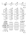
- the high-voltage switch according to the invention in FIG. 1 consists of several groups (10, 20, 30, 40) (11, 21, 31, 41), ..., (1N, 2N, 3N, 4N) of four semiconductor switches connected in series as examples.
- a control line ST10-ST1N leads to each of these groups, via which control pulses of the control circuit S are transmitted.
- FIG. 1 shown basic circuit of series-connected semiconductor switches can be trained in various ways and adapted to the different applications.
- a series can be made from the two basic circuits of a plurality of semiconductor switches connected in series or a plurality of semiconductor switches connected in parallel, as are shown in FIGS. 2 and 5 by way of example using four components 10-40 or 10-30 connected in series or three in parallel derived from configurations consisting of groups of semiconductor switches connected in series or in parallel, such as, for example, the configurations in FIGS. 3 and 4 which result from the series connection of FIG. 2 are derived, or that in FIGS. 6 and 7, which result from the parallel connection of FIG. 5 are derived.
- the individual semiconductor switches are represented by circles in all of FIGS. 2-7, one circle in each of FIGS. 2 and 5 being filled with the circuit symbols of a MOSFET representative of all other circles, which should however only be understood as a general symbol for a semiconductor switch.
- each semiconductor switch 10-40 of FIG. 2 exemplarily four further switches 11-14; 21-24; 31-34; 41-44 connected in parallel, in FIG. 4 each of the semiconductor switches 10-14; 20-24; 30-34; 40-44 of FIG. 3 exemplarily two further switches 10a, b; 11a, b; ..44a, b connected in series.
- each semiconductor switch 10-30 of FIG. 5 exemplarily three further switches 11-13; 21-23; 31-33 connected in series, in FIG. 7 each of the semiconductor switches 10-13; 20-23; 30-33 of FIG. 6 exemplarily two further switches 10a, b; 11a, b; ... 33a, b connected in parallel.
- Other configurations are of course also possible.
- FIGS. 8-12 Preferred embodiments of the controls according to the invention for groups of series-connected MOSFETs are shown in FIGS. 8-12.
- FIG. 8 shows an example of a group of four MOSFETs 10-40 connected in series.
- Each of these MOSFETs 10-40 is connected with its gate electrode in a manner known per se from EP-A1-0 048 758 to a control line ST10-ST40 assigned to it.
- a transformer preferably a toroidal transformer U10-U40 is provided in the control lines ST10-ST40, the secondary winding of which is connected to the gate electrode at one end and to the source electrode of the associated MOSFET 10 at the other end -40 is connected and its primary winding is connected at one end to ground and the other end to the assigned control line ST10-ST40.
- an additional variable value R10-R40 is installed in each control line ST10-ST40, which is in series with the primary winding of the assigned transformer Ü10-Ü40.
- a variably adjustable time delay element (not shown in the figure) can also be installed in each control line ST10-ST40, which is preferably also connected in series with the primary winding of the assigned transformer U10-U40.
- FIG. 9 shows, by way of example, a group of four MOSFETs 10-40 connected in series, of which only the MOSFET 10 is directly controlled via a control line ST 10, while the control of the remaining MOSFET 20-40 via an RC voltage divider R50-R80, C20 -C40 is done.
- the MOSFET 10 is closest to the minus reference potential of the series circuit at point P10, while the MOSFET 40 is closest to the plus reference potential of the series circuit at point P20.
- the gate electrodes of the individual MOSFETs 10-40 are each connected to a current limiting resistor R10-R40.
- Zener diodes Z10-Z40 are provided, each of which connects the source electrode of the associated MOSFET 10-40 to its gate electrode.
- the RC voltage divider consists of a series connection of preferably identical resistors R50-R80 and a parallel connection of capacitors C20-C40, which are connected at one end to the minus reference potential of the MOSFET series connection and at the other end to each the connection points P11-P13 between the resistors R50-R80 of the RC voltage divider.
- An auxiliary voltage source B1 and B2 with its positive pole is connected to the two ends of the resistance series circuit R50-R80, while the negative pole of the auxiliary voltage source B1 is connected to the negative reference potential P10 and that of the auxiliary voltage source B2 to the positive reference potential P20 of the MOSFET - Series connection are connected.
- the two auxiliary voltage sources B1 and B2 are required in order to achieve the lowest possible residual voltage at the switched-through MOSFETs 10-40.
- the passage The voltage of a MOSFET is typically less than 6V.
- the gate voltage required for this is typically 10V.
- auxiliary voltage sources Without auxiliary voltage sources, a residual voltage would statically arise at each MOSFET 10-40 in the amount of the required gate voltage, i.e. 10V.
- the residual voltage is statically dependent only on the current and on resistance R ON of the MOSFETs 10-40.
- the static distribution of the reverse voltage depends on the resistors R50-R80 of the RC voltage divider. If the voltage divider consists of the same resistors R50-R80 and the blocking resistances of the MOSFETs 10-40 are high, then the blocking voltage distribution on the MOSFETs 10-40 is ideally the same.
- MOSFET 20 in FIG. 9 Has a MOSFET, e.g. MOSFET 20 in FIG. 9, a low blocking resistance or is alloyed, then the blocking voltage of the defective MOSFET 20 and that of the MOSFETs 30 and 40 which are potentially above it decrease. In the extreme case, the reverse voltage is only distributed via the MOSFETs (potentially MOSFET 10) below it, which can lead to the destruction of the components.
- the gate connection Since, when a MOSFET is destroyed, the gate connection also has a low-resistance connection to the drain and source connection of the component, the gate-source voltage cannot be reversed and there is no possibility of a MOSFET's drain-source short-circuit Measurement and Evaluation of the gate voltage to make the potential overlying MOSFETs lockable by short-circuiting the associated resistor in the voltage divider.
- the capacitances C GS and C GD In order to be able to switch a MOSFET on and off quickly, the capacitances C GS and C GD must be reloaded accordingly quickly.
- the capacitance C GD of a MOSFET is voltage-dependent.
- a MOSFET with a relatively low control current can be switched on, but in order to achieve the residual voltage specified in the data sheet of the component, the control current generally has to be increased by more than 50%.
- the capacitors C GS and C GD of a MOSFET are charged and discharged by means of an external capacitor connected to the negative reference potential. If the current flow to the negative reference potential is interrupted, then the current flows via C GD and C GS to the outer capacitor, the capacitance of which must be selected so that a sufficient charge reversal of C GD and C GS is possible.
- the capacitors C20-C40 correspond to this outer capacitor in FIGS. 9 and 10.
- the MOSFET 10 closest in potential to the minus reference potential P10 is replaced by a via the control Line ST10 transmitted control pulse switched on by the external control circuit (S in FIG. 1), then the current flows from the external capacitors C20-C40 of the RC voltage divider via the transistor capacitances C GS and C GD of the other MOSFETs 20-40 of the MOSFET Series connection and thereby turns on the entire MOSFET chain 10-40.
- the capacitance of the capacitors C20-C40 depends on which of the MOSFETs 10-40 they are connected to and how they are connected to the negative reference potential P10 of the transistor chain.
- the function of the two circuits in FIG. 9 and 10 is otherwise the same.
- An advantageous embodiment of the circuit shown in FIG. 10 is shown in FIG. 11 shown.
- the auxiliary voltage source B2 of FIG. 10 is shown in FIG. 11 in the form of a current transformer T2 with a rectifier arrangement G2 connected downstream, which is followed by a Zener diode Z2 bridged by a capacitor E2.
- the auxiliary voltage source B1 connected to the negative reference potential P10 is also realized in the form of a Zener diode Z1, which is bridged by a capacitor E1. Since, in this exemplary embodiment, the MOSFET 10 closest in potential to the minus reference potential P10 is potential-free (here, for example, via an optical fiber cable L1 with upstream and downstream electro-optical converters OE1 and OE2), the operating voltage for the control module OP1 can only be obtained initially from this lower auxiliary voltage source Z1, E1 are taken, which is effective when the high voltage to be switched is applied, so that switching the MOSFET series circuit 10-40 is possible for a short time. The further supply then takes place via a current transformer T1 with a rectifier arrangement G1 connected downstream.
- the two control lines each contain a pulse transformer U10 or U11 for electrical isolation, a variable value R10 or R11 and possibly also a time delay element (not shown), so that this part of the circuit is comparable to the control of a MOSFETs in the circuit according to FIG. 8.
- the remaining MOSFETs 20-30 and 21-31 of the two groups are, however, as in the circuits shown in FIG. 10 and 11 each controlled by an RC voltage divider.
- MOSFETs To implement a 30 kV high-voltage switch, approximately 60-70 800 V MOSFETs must be connected in series, taking into account a sufficient safety factor.
- these MOSFETs can be divided into 6-7 groups, each with 10 MOSFETs, 9 of which are controlled by an RC voltage divider, while the lowest potential MOSFET of each group via fiber optic cables, carrier frequency or with needle pulses from the external control circuit (S in FIG. 1) is driven, so that a total of only seven control channels are required for seventy MOSFETs.
- the potential of the highest MOSFET in each group is monitored for its switching state, since if a MOSFET within this group fails, this MOSFET is always also affected.
- FIG. 13 shows a group of four MOSFETs 10-40 to be monitored, the control of which (not shown completely), for example the control according to FIG. 11 corresponds and among other things contains a light guide cable L1 with a downstream electro-optical converter OE 2 for transmitting the control pulses and a control module OP1 which is connected via a current limiting resistor R10 to the gate electrode of the MOSFET 10 closest to the minus reference potential P10 and which is supplied by an auxiliary voltage source B5 .
- the monitoring device is connected with one of its two inputs at the connection points P20 and P15 to the drain or source electrode of the MOSFET 40 which is potentially closest to the plus reference potential.
- the inputs are connected via capacitors CA and CB to the ends of the primary winding of a transformer T3, whose center tap is connected to the negative reference potential P10 of the MOSFET series circuit.
- the secondary Winding of the transformer T3 is also directly connected at one end and at the other end via a series connection of diode D and capacitor C to the negative reference potential P10.
- a tap is provided between diode D and capacitor C, which is connected via a resistor R to a comparator K1, which is also supplied by the auxiliary voltage source B5.
- the comparator K1 is connected on the output side to an electro-optical converter OE3, the output of which is connected via a second light guide cable L2 to an evaluation unit (not shown) in the control circuit (S in FIG. 1)
- the monitoring device according to the invention in FIG. 14 differs from the device in FIG. 13 in that the capacitor CB is connected via a series resistor RB, RC and the capacitor CA is connected via a resistor RA to the negative reference potential P10 of the series MOSFET. Taps are provided between the capacitor CA and the resistor RA and between the two resistors RB and RC, which are connected to the inputs of a differential amplifier DV, which is supplied by an auxiliary voltage source B6. On the output side, the differential amplifier DV is again connected to an electro-optical converter OE3, the output of which is connected to the evaluation unit (not shown) via a second light guide cable.
- FIG. 15 A third embodiment of the monitoring device according to the invention is shown in FIG. 15 shown. It consists in essentially from a comparator K2, which is connected on the input side to the source electrode of the MOSFET 40 which is closest in potential to the plus reference potential P20 of the MOSFET series circuit and which is shown in FIG. 11, the auxiliary voltage source B2 shown in detail is supplied, which is implemented in the form of a current transformer T2 with a rectifier arrangement G2 connected downstream, which is followed by a Zener diode Z2 bridged with an (electrolytic) capacitor E2.
- the comparator K2 is again connected to an electro-optical converter OE3, the output of which is connected to the evaluation unit (not shown) via a second optical fiber cable L2.
- the capacitors C A and C B are the same size, then if a transistor fails, the capacitors (CA or CB) flowing currents in the transformer T3 and the secondary voltage is zero. In practice, the tension decreases by about 30-50%.
- the voltage measured at the drain terminal of the uppermost transistor 40 behind the capacitor CB is divided in such a way that a voltage can be measured between RB and RC which corresponds to the value which occurs when measuring the drain voltage of the penultimate transistor 30 behind the capacitor CA at RA .
- the differential voltage is zero. If a transistor in the MOSFET series circuit fails, the differential voltage is not equal to zero and the connected differential amplifier DV can emit an error message which, as shown in FIG. 13, via the electro-optical converter OE3 and the light guide cable L2 (or alternatively via a pulse transmitter by means of carrier frequency) to the evaluation unit in the control circuit, for example to ground potential.
- the switching voltage of the uppermost transistor 40 is evaluated directly by a comparator K2, which, when falling below a threshold, reports a switching voltage that is too low, for example via the electro-optical converter OE3 and fiber optic cable L2 (or alternatively via a pulse transmitter using carrier frequency) to the evaluation unit in the control circuit.
- the monitoring circuits for the individual MOSFET groups can each be supplied by the same auxiliary voltage source (B1 in FIGS. 9 and 10) with which the signal receiver (OP1 in FIG. 11) is also used to control the MOSFET (10 in the Figures 10-12) is operated.
- the auxiliary voltage source can - as discussed above - be powered when switching on from the resistor divider and then from a current transformer.
- the error feedback can be used for further evaluation e.g. can be transmitted to earth potential via fiber optic cables, carrier frequency or pulse transmitters.
- the switch according to the invention can generally be used where high direct voltages have to be switched on and off. It is particularly suitable for use in all the applications in which previously expensive and wear-sensitive switching tubes, in particular high-performance switching tubes, had to be used.
- Examples of this are high-voltage direct current supplies, in particular for the power supply of magnets in particle accelerator systems or modulation amplifiers for transmitters, in particular modulation amplifiers for amplitude-modulated high-power transmitters in the long, medium and short-wave range, the RF output stage of which are still equipped today with a mostly anode-modulated RF power tube , for which modulation voltages up to 30-50 KV are required.
- Such a modulation amplifier consists of a switching amplifier and a low-pass filter.
- the switching amplifier is driven by a sequence of pulses which result from the modulating analog low frequency input signal can be derived.
- the pulse or switching frequency ie the number of pulses per unit of time with a constant pulse duration and amplitude, is proportional to the amplitude of the input signal or the pulse duration with a constant pulse frequency and amplitude.
- PFM pulse frequency modulation
- PDM pulse duration modulation
- Such a modulation amplifier for example pulse duration modulated pulses (“pulse duration modulation amplifier” or “PDM amplifier” for short) is only able due to its circuit principle to deliver an output voltage U A to the RF part that is less than the input voltage U B is.
- the setting range is between 0 and 100% of the input voltage U B , and any value of U A between 0 and 100% of U B can be set statically or dynamically.
- the modulation amplifier thus has a lower cut-off frequency of 0 Hz and thus the property of a DC voltage transformer.
- the modulation amplifier supplies both the carrier power and the modulation power for the RF part of the amplitude-modulated transmitter, its input voltage U B must be equal to the maximum anode voltage of the anode-modulated RF power amplifier tube in the RF part.
- the high demands on such an amplifier with regard to its output values (power, voltage, current etc.) and its quality values (distortion factor, etc.) and its efficiency previously required the use of a switching tube.
- This switching tube can advantageously be replaced by the high-voltage switch according to the invention.
- the structure of the modulation amplifier is simplified, and on the other hand, its reliability is increased by using semiconductor switches instead of the wear-sensitive switching tube.
- the spare parts and valuation costs are reduced, since there is no (usually annual) exchange of the switching tube.
- the tube for the RF output stage that will also be needed in the future, at least in short-wave transmitters, can now be selected purely according to RF criteria. It is no longer necessary to use a tube that also meets the requirements in the modulation amplifier.
- the heating transformer, the screen grid power supply and the complex driver stage for the switching tube are omitted, which is associated with a corresponding cost saving in manufacture.
- a further considerable cost saving arises from the fact that instead of the expensive memory coil with two windings conventionally used previously as a filter choke in the low-pass filter of the modulation amplifier, a conventional memory choke with only one winding can now be used.
- the storage choke due to the short discharge times (which are generally shorter than the dead times between the switching operations of the two switches) and is consumed in the load resistor and is diverted via the second switch only in the case of an underscore (ie in the case of small current values or longer discharge times) and is consumed in a resistor connected in series with the second switch.
- the additional switch can be constructed with semiconductor switches of lower switching capacity, which generally Have shorter switching times, so that the losses in the additional switch can be reduced even further.
Landscapes
- Engineering & Computer Science (AREA)
- Power Engineering (AREA)
- Electronic Switches (AREA)
Applications Claiming Priority (2)
| Application Number | Priority Date | Filing Date | Title |
|---|---|---|---|
| DE3822991 | 1988-07-07 | ||
| DE19883822991 DE3822991A1 (de) | 1988-07-07 | 1988-07-07 | Hochspannungsschalter |
Publications (1)
| Publication Number | Publication Date |
|---|---|
| EP0353406A1 true EP0353406A1 (fr) | 1990-02-07 |
Family
ID=6358146
Family Applications (1)
| Application Number | Title | Priority Date | Filing Date |
|---|---|---|---|
| EP89108573A Withdrawn EP0353406A1 (fr) | 1988-07-07 | 1989-05-12 | Commutateur pour tensions élevées |
Country Status (2)
| Country | Link |
|---|---|
| EP (1) | EP0353406A1 (fr) |
| DE (1) | DE3822991A1 (fr) |
Cited By (12)
| Publication number | Priority date | Publication date | Assignee | Title |
|---|---|---|---|---|
| EP0924844A1 (fr) * | 1997-12-18 | 1999-06-23 | Commissariat A L'energie Atomique | Interrupteur haute tension réalisé à partir de cellules quasi-résonantes connectées en série |
| FR2773011A1 (fr) * | 1997-12-18 | 1999-06-25 | Commissariat Energie Atomique | Interrupteur haute tension realise a partir de cellules a deux interrupteurs aides a la fermeture et a l'ouverture, connectees en serie |
| FR2773010A1 (fr) * | 1997-12-18 | 1999-06-25 | Commissariat Energie Atomique | Interrupteur haute tension realise a partir de cellules resonantes connectees en serie |
| US6304475B1 (en) | 1998-06-16 | 2001-10-16 | Mitsubishi Denki Kabushiki Kaisha | Switching power supply for gas laser |
| DE10042292A1 (de) * | 2000-08-29 | 2002-03-21 | Tuilaser Ag | Excimer-Laser |
| WO2004086614A1 (fr) * | 2003-03-21 | 2004-10-07 | D2Audio Corporation | Synchronisation et communication pwm multipuce |
| WO2009066274A1 (fr) * | 2007-11-20 | 2009-05-28 | Ferfics Limited | Surveillance de circuit de distribution de puissance |
| US7584009B2 (en) | 2003-03-21 | 2009-09-01 | D2Audio Corporation | Multi-chip PWM synchronization and communication |
| DE102009017543A1 (de) | 2009-04-17 | 2010-10-21 | Dspace Digital Signal Processing And Control Engineering Gmbh | Schalter |
| US7929718B1 (en) | 2003-05-12 | 2011-04-19 | D2Audio Corporation | Systems and methods for switching and mixing signals in a multi-channel amplifier |
| WO2015090440A1 (fr) * | 2013-12-20 | 2015-06-25 | Abb Technology Ltd | Agencement disjoncteur |
| EP3614562A1 (fr) * | 2018-08-24 | 2020-02-26 | General Electric Technology GmbH | Appareil de soupape électronique |
Families Citing this family (2)
| Publication number | Priority date | Publication date | Assignee | Title |
|---|---|---|---|---|
| US5258994A (en) * | 1990-06-20 | 1993-11-02 | Mitsubishi Denki K.K. | Discharge-excited laser apparatus |
| US5305338A (en) * | 1990-09-25 | 1994-04-19 | Mitsubishi Denki Kabushiki Kaisha | Switch device for laser |
Citations (11)
| Publication number | Priority date | Publication date | Assignee | Title |
|---|---|---|---|---|
| US3184615A (en) * | 1963-01-14 | 1965-05-18 | Hughes Aircraft Co | Pulse modulator with transistor switch |
| CH451315A (de) * | 1967-02-10 | 1968-05-15 | Bbc Brown Boveri & Cie | Umrichteranordnung mit mehreren in Reihe liegenden gesteuerten Stromrichterelementen |
| US3510687A (en) * | 1966-08-23 | 1970-05-05 | Comp Generale Electricite | Control arrangement for series connected thyristors |
| US3526787A (en) * | 1966-11-17 | 1970-09-01 | Hughes Aircraft Co | Complementary transistor pair switching circuit |
| GB1269502A (en) * | 1968-05-16 | 1972-04-06 | English Electric Co Ltd | Improvements in thyristor firing circuits |
| DE3125242A1 (de) * | 1980-06-27 | 1982-03-04 | Kabushiki Kaisha Morita Seisakusho, Kyoto | "gate-treibschaltung fuer einen static-induction-transistor (sit)" |
| EP0048758A1 (fr) * | 1979-12-28 | 1982-04-07 | International Rectifier Corporation Japan, Ltd. | Configuration de circuit de transistor a effet de champ |
| EP0140349A2 (fr) * | 1983-10-28 | 1985-05-08 | Hitachi, Ltd. | Dispositif de commutation à semi-conducteurs |
| JPS61102816A (ja) * | 1984-10-25 | 1986-05-21 | Hitachi Ltd | 半導体スイツチ回路 |
| EP0215707A1 (fr) * | 1985-09-06 | 1987-03-25 | Thomson-Csf | Dispositif de commutation de tension |
| EP0226006A1 (fr) * | 1985-11-26 | 1987-06-24 | Licentia Patent-Verwaltungs-GmbH | Amplificateur à commutation pour signaux analogiques basse fréquence |
-
1988
- 1988-07-07 DE DE19883822991 patent/DE3822991A1/de not_active Withdrawn
-
1989
- 1989-05-12 EP EP89108573A patent/EP0353406A1/fr not_active Withdrawn
Patent Citations (11)
| Publication number | Priority date | Publication date | Assignee | Title |
|---|---|---|---|---|
| US3184615A (en) * | 1963-01-14 | 1965-05-18 | Hughes Aircraft Co | Pulse modulator with transistor switch |
| US3510687A (en) * | 1966-08-23 | 1970-05-05 | Comp Generale Electricite | Control arrangement for series connected thyristors |
| US3526787A (en) * | 1966-11-17 | 1970-09-01 | Hughes Aircraft Co | Complementary transistor pair switching circuit |
| CH451315A (de) * | 1967-02-10 | 1968-05-15 | Bbc Brown Boveri & Cie | Umrichteranordnung mit mehreren in Reihe liegenden gesteuerten Stromrichterelementen |
| GB1269502A (en) * | 1968-05-16 | 1972-04-06 | English Electric Co Ltd | Improvements in thyristor firing circuits |
| EP0048758A1 (fr) * | 1979-12-28 | 1982-04-07 | International Rectifier Corporation Japan, Ltd. | Configuration de circuit de transistor a effet de champ |
| DE3125242A1 (de) * | 1980-06-27 | 1982-03-04 | Kabushiki Kaisha Morita Seisakusho, Kyoto | "gate-treibschaltung fuer einen static-induction-transistor (sit)" |
| EP0140349A2 (fr) * | 1983-10-28 | 1985-05-08 | Hitachi, Ltd. | Dispositif de commutation à semi-conducteurs |
| JPS61102816A (ja) * | 1984-10-25 | 1986-05-21 | Hitachi Ltd | 半導体スイツチ回路 |
| EP0215707A1 (fr) * | 1985-09-06 | 1987-03-25 | Thomson-Csf | Dispositif de commutation de tension |
| EP0226006A1 (fr) * | 1985-11-26 | 1987-06-24 | Licentia Patent-Verwaltungs-GmbH | Amplificateur à commutation pour signaux analogiques basse fréquence |
Cited By (23)
| Publication number | Priority date | Publication date | Assignee | Title |
|---|---|---|---|---|
| FR2773011A1 (fr) * | 1997-12-18 | 1999-06-25 | Commissariat Energie Atomique | Interrupteur haute tension realise a partir de cellules a deux interrupteurs aides a la fermeture et a l'ouverture, connectees en serie |
| FR2773009A1 (fr) * | 1997-12-18 | 1999-06-25 | Commissariat Energie Atomique | Interrupteur haute tension realise a partir de cellules quasi-resonantes connectees en serie |
| FR2773010A1 (fr) * | 1997-12-18 | 1999-06-25 | Commissariat Energie Atomique | Interrupteur haute tension realise a partir de cellules resonantes connectees en serie |
| EP0928057A1 (fr) * | 1997-12-18 | 1999-07-07 | Commissariat A L'energie Atomique | Interrupteur haute tension realisé à partir de cellules resonantes connectées en serie |
| EP0924844A1 (fr) * | 1997-12-18 | 1999-06-23 | Commissariat A L'energie Atomique | Interrupteur haute tension réalisé à partir de cellules quasi-résonantes connectées en série |
| US6304475B1 (en) | 1998-06-16 | 2001-10-16 | Mitsubishi Denki Kabushiki Kaisha | Switching power supply for gas laser |
| DE19917591B4 (de) * | 1998-06-16 | 2007-06-21 | Mitsubishi Denki K.K. | Laser-Stromversorgungsgerät |
| DE10042292A1 (de) * | 2000-08-29 | 2002-03-21 | Tuilaser Ag | Excimer-Laser |
| DE10042292B4 (de) * | 2000-08-29 | 2004-08-12 | Tuilaser Ag | Verfahren zum Betreiben eines Excimer-Laser |
| WO2004086614A1 (fr) * | 2003-03-21 | 2004-10-07 | D2Audio Corporation | Synchronisation et communication pwm multipuce |
| US7584009B2 (en) | 2003-03-21 | 2009-09-01 | D2Audio Corporation | Multi-chip PWM synchronization and communication |
| US7929718B1 (en) | 2003-05-12 | 2011-04-19 | D2Audio Corporation | Systems and methods for switching and mixing signals in a multi-channel amplifier |
| WO2009066274A1 (fr) * | 2007-11-20 | 2009-05-28 | Ferfics Limited | Surveillance de circuit de distribution de puissance |
| US8570025B2 (en) | 2007-11-20 | 2013-10-29 | Ferfics Limited | Power delivery circuit with load current estimation based on monitoring nodes not on the power delivery path |
| DE102009017543A1 (de) | 2009-04-17 | 2010-10-21 | Dspace Digital Signal Processing And Control Engineering Gmbh | Schalter |
| WO2015090440A1 (fr) * | 2013-12-20 | 2015-06-25 | Abb Technology Ltd | Agencement disjoncteur |
| CN106463949A (zh) * | 2013-12-20 | 2017-02-22 | Abb技术有限公司 | 电路断路布置 |
| US9705312B2 (en) | 2013-12-20 | 2017-07-11 | Abb Schweiz Ag | Circuit breaking arrangement |
| CN106463949B (zh) * | 2013-12-20 | 2018-06-01 | Abb瑞士股份有限公司 | 电路断路布置 |
| EP3614562A1 (fr) * | 2018-08-24 | 2020-02-26 | General Electric Technology GmbH | Appareil de soupape électronique |
| WO2020038796A1 (fr) * | 2018-08-24 | 2020-02-27 | General Electric Technology Gmbh | Appareil à valve électronique |
| CN112868179A (zh) * | 2018-08-24 | 2021-05-28 | 通用电器技术有限公司 | 电子阀装置 |
| US11777307B2 (en) | 2018-08-24 | 2023-10-03 | General Electric Technology Gmbh | Electronic valve apparatus |
Also Published As
| Publication number | Publication date |
|---|---|
| DE3822991A1 (de) | 1990-01-11 |
Similar Documents
| Publication | Publication Date | Title |
|---|---|---|
| DE3877326T2 (de) | Leistungsversorgung. | |
| DE10214190B4 (de) | Stromversorgung mit mehreren parallel geschalteten Schaltnetzteilen | |
| DE60034955T2 (de) | Spannungsabgleich in zwischenkreiskondensatoren | |
| EP0353406A1 (fr) | Commutateur pour tensions élevées | |
| EP1526633A2 (fr) | Circuit fournissant un courant alternatif | |
| DE3407067A1 (de) | Steuerschaltung fuer gasentladungslampen | |
| DE102008005312B4 (de) | Optimiertes Widerstandsnetzwerk für programmierbare Transkonduktanzstufe | |
| DE60205058T2 (de) | Schaltnetzteil | |
| EP0437884A2 (fr) | Convertisseur de tension continu à récupération | |
| DE102010048951A1 (de) | Stromquelle mit Dimmvorrichtung | |
| EP0287166A2 (fr) | Circuit de limitation des pointes de courant pour un transistor de commutation | |
| DE10328782A1 (de) | Steuerschaltung für einen MOSFET zur Synchrongleichrichtung | |
| EP0201878A2 (fr) | Circuit à transistor MOS à canal N commutant un potentiel positif | |
| AT516903B1 (de) | Schaltungsanordnung mit Transformator mit Mittelpunktanzapfung und Messung der Ausgangsspannung | |
| EP1195885B1 (fr) | Circuit redresseur synchrone | |
| EP0327682A1 (fr) | Amplificateur à commutation pour amplification numérique de puissance | |
| EP0353403A1 (fr) | Amplificateur à modulation pour tensions élevées | |
| DE2641912B2 (de) | Schaltungsanordnung zur Übertragung elektrischer Versorgungsleistungen | |
| EP0048490B1 (fr) | Circuit pour transformer un signal d'entrée binaire en un signal télégraphique | |
| AT516641B1 (de) | Schaltungsanordnung zur Symmetrierung von Zwischenkreiskondensatoren | |
| DE69700066T2 (de) | Regelvorrichtung einer Niederdruckleuchtstofflampe | |
| DE2647958A1 (de) | Schaltungsanordnung fuer einen gegentakt-wechselrichter mit einer regeleinrichtung fuer den gegentakt | |
| EP2208402B1 (fr) | Ballast pour lampe à décharge, par exemple pour une lampe dhi | |
| DE3521169C2 (fr) | ||
| DE2856566C2 (de) | Laufzeitketten-Pulsmodulator |
Legal Events
| Date | Code | Title | Description |
|---|---|---|---|
| PUAI | Public reference made under article 153(3) epc to a published international application that has entered the european phase |
Free format text: ORIGINAL CODE: 0009012 |
|
| AK | Designated contracting states |
Kind code of ref document: A1 Designated state(s): CH DE FR GB LI |
|
| ITCL | It: translation for ep claims filed |
Representative=s name: RICCARDI SERGIO & CO. |
|
| 17P | Request for examination filed |
Effective date: 19900301 |
|
| 17Q | First examination report despatched |
Effective date: 19901026 |
|
| STAA | Information on the status of an ep patent application or granted ep patent |
Free format text: STATUS: THE APPLICATION IS DEEMED TO BE WITHDRAWN |
|
| 18D | Application deemed to be withdrawn |
Effective date: 19911211 |