EP0353519A2 - Geschütztes Gerät zum Befehlsvorausholen - Google Patents
Geschütztes Gerät zum Befehlsvorausholen Download PDFInfo
- Publication number
- EP0353519A2 EP0353519A2 EP89112835A EP89112835A EP0353519A2 EP 0353519 A2 EP0353519 A2 EP 0353519A2 EP 89112835 A EP89112835 A EP 89112835A EP 89112835 A EP89112835 A EP 89112835A EP 0353519 A2 EP0353519 A2 EP 0353519A2
- Authority
- EP
- European Patent Office
- Prior art keywords
- cpu
- signal
- instruction
- memory
- signals
- Prior art date
- Legal status (The legal status is an assumption and is not a legal conclusion. Google has not performed a legal analysis and makes no representation as to the accuracy of the status listed.)
- Withdrawn
Links
Images


Classifications
-
- G—PHYSICS
- G06—COMPUTING OR CALCULATING; COUNTING
- G06F—ELECTRIC DIGITAL DATA PROCESSING
- G06F9/00—Arrangements for program control, e.g. control units
- G06F9/06—Arrangements for program control, e.g. control units using stored programs, i.e. using an internal store of processing equipment to receive or retain programs
- G06F9/30—Arrangements for executing machine instructions, e.g. instruction decode
- G06F9/38—Concurrent instruction execution, e.g. pipeline or look ahead
- G06F9/3802—Instruction prefetching
-
- G—PHYSICS
- G06—COMPUTING OR CALCULATING; COUNTING
- G06F—ELECTRIC DIGITAL DATA PROCESSING
- G06F11/00—Error detection; Error correction; Monitoring
- G06F11/004—Error avoidance
-
- G—PHYSICS
- G06—COMPUTING OR CALCULATING; COUNTING
- G06F—ELECTRIC DIGITAL DATA PROCESSING
- G06F11/00—Error detection; Error correction; Monitoring
- G06F11/07—Responding to the occurrence of a fault, e.g. fault tolerance
- G06F11/0703—Error or fault processing not based on redundancy, i.e. by taking additional measures to deal with the error or fault not making use of redundancy in operation, in hardware, or in data representation
- G06F11/0751—Error or fault detection not based on redundancy
- G06F11/0754—Error or fault detection not based on redundancy by exceeding limits
- G06F11/0757—Error or fault detection not based on redundancy by exceeding limits by exceeding a time limit, i.e. time-out, e.g. watchdogs
-
- G—PHYSICS
- G06—COMPUTING OR CALCULATING; COUNTING
- G06F—ELECTRIC DIGITAL DATA PROCESSING
- G06F11/00—Error detection; Error correction; Monitoring
- G06F11/07—Responding to the occurrence of a fault, e.g. fault tolerance
- G06F11/0703—Error or fault processing not based on redundancy, i.e. by taking additional measures to deal with the error or fault not making use of redundancy in operation, in hardware, or in data representation
- G06F11/0751—Error or fault detection not based on redundancy
- G06F11/0763—Error or fault detection not based on redundancy by bit configuration check, e.g. of formats or tags
Definitions
- This invention relates to microprocessors and associated memories and is especially adapted for use with a single chip MCU.
- Single chip MCUs are utilized in IC cards, such as bank cards, credit cards, etc.
- a time-out timer is connected to the CPU of a microprocessor so as to reset the CPU if the timer is allowed to time-out.
- a main problem caused by a watchdog timer is that it prohibits execution of underfined instructions. Further, in the event of a low supply voltage condition, which often and easily happens in IC cards, the timer is one of the first circuits to be effected and, therefore, operation is effectively prohibited under these conditions.
- a microprocessor including a CPU including means for fetching selected instructions from a memory, a memory for storing a plurality of instructions and connected to said CPU for supplying selected instructions in response to fetch signals, signal circuitry coupled to said memory and CPU for providing a second signal when a selected signal instruction is available for fetching, and logic circuitry connected to receive the fetch and second signals and further connected to the CPU for inhibiting operation when the fetch and second signals are not both present.
- FIG. 1 illustrates a central processing unit (CPU) 10 having an address decoder 12, a random access memory (RAM) 14, a data read-only-memory (ROM) 16, and an instruction ROM 18 connected thereto by means of an address bus 20 and a data bus 22.
- a system clock (not shown) supplies timing pulses to CPU 10 and address decoder 12.
- CPU 10 includes a timing sequencer 24 which supplies an instruction fetch signal to an instruction latch 26 upon the completion of each instruction in an operation.
- Instruction latch 26 receives (fetches) the next instruction from instruction ROM 18.
- An instruction is fetched by sending an address to address decoder 12 and memories 14, 16, and 18 by way of address bus 20.
- Address decoder 12 determines that it is an address for instruction ROM 18 and sends a chip enable signal, CE , to instruction ROM 18. With the enable signal and address applied to instruction ROM 18, the selected instruction is supplied to instruction latch 26 by way of data bus 22.
- CE chip enable signal
- the problem that arises is that power supply voltage drops, incoming noises, software errors, etc. can cause a malfunction. If such a malfunction occurs, the microprocessor may overrun and continue to operate using wrong instructions. When this occurs the microprocessor is running out of function and doesn't return to the proper function. In such instances the microprocessor can be destroyed. Also, persons wanting to learn the program may be able to access memories 14, 16, and 18 or insert incorrect instructions.
- a logic circuit 30 is connected to CPU 10 and address decoder 12.
- Logic circuit 30 includes an OR gate 32 and an AND gate 34.
- An output of OR gate 32 is connected to the reset input of CPU 10.
- a first input of OR gate 32 is connected to receive reset signals from external hardware in the normal fashion.
- a second input of OR gate 32 is connected to receive reset signals from the output of AND gate 34.
- a first input of AND gate 34 is connected to receive the instruction fetch signal from timing sequencer 24.
- a second input of AND gate 34 is connected to receive the chip enable signal from address decoder 12.
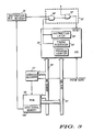
- FIG. 3 illustrates a second embodiment of the invention. Parts similar in connection and operation to those described in FIG. 1 are numbered with similar numbers, but a prime is added to indicate 8 different embodiment.
- information ROM 18′ may contain instructions and bytes of data and has additional memory 18A, which may be part of the same ROM or an additional component.
- An instruction bit decoder 36 receives identification bits from additional memory 18A whenever information bytes in information ROM 18′ are accessed. Detector 36 determines from the identification bits whether it is an instruction that has been accessed and, if it is, sends a signal to the second input of AND gate 34′. This input of AND gate 34′ is not connected to address decoder 12′ in this embodiment.
- timing sequencer 24 sends a fetch signal to instruction latch 26, the fetch signal is also supplied to the first input of AND gate 34.
- the addresss for the selected instruction is sent by address bus 20 to address decoder 12 and memories 14, 16, and 18.
- Address decoder 12 detects the address and sends CE signal to instruction ROM 18 and to the second input of AND gate 34.
- the instruction is available for fetching by CPU 10.
- ROM 18 is enabled by CE and sends the selected instruction to instruction latch 26 by way of data bus 22.
- CE which is a low level signal (see FIG. 2), prevents AND gate 34 from supplying an error signal to OR gate 32.
- CPU 10 sends a fetch signal and the correct address is not detected by address decoder 12, CE will not be generated and AND gate 34 will produce an error signal which will reset CPU 10. Any attempts, either intentional or accidental, to improperly sequence the data or instructions will result in CPU 10 being inhibited. Thus, overruns and other improper functions are inhibited.
- timing sequencer 24′ supplies a fetch signal to AND gate 34′. Simultaneously, the address of the selected instruction is sent to address decoder 12′ and ROM 18′. Rddress decoder 12′ enables ROM 18′ and the selected instruction is supplied to CPU 10′ by way of data bus 22′. Also, one or more identifier bits, associated with the selected instruction, are sent to instruction bit decoder 36 from additional memory 18A. If the identifier bits are detected as identifying an instruction byte, (i.e. an instruction is available) detector 36 sends a low level signal to AND gate 34′ to prevent it from sending an error signal to OR gate 32′. The identifier bits can be virtually and desired code which will identify the fact that an instruction byte (and not a data byte, etc.) has been sent by ROM 18′.
- this invention prevents overruns and operation of a microprocessor out of function.
- the invention increases copy protection and reliability since the CPU will be reset if the proper instructions are not supplied at the correct times. Further, if a power supply voltage drop, incoming noise, software errors, etc. cause a malfunction between the CPU and the associated memories, the CPU will be reset.
- This invention is especially suitable for use with single chip microprocessors, such as in IC cards and the like.
Landscapes
- Engineering & Computer Science (AREA)
- Theoretical Computer Science (AREA)
- Software Systems (AREA)
- Physics & Mathematics (AREA)
- General Engineering & Computer Science (AREA)
- General Physics & Mathematics (AREA)
- Quality & Reliability (AREA)
- Debugging And Monitoring (AREA)
- Advance Control (AREA)
- Storage Device Security (AREA)
- Executing Machine-Instructions (AREA)
Applications Claiming Priority (2)
| Application Number | Priority Date | Filing Date | Title |
|---|---|---|---|
| JP194382/88 | 1988-08-05 | ||
| JP63194382A JPH0244431A (ja) | 1988-08-05 | 1988-08-05 | 保護命令取出し装置 |
Publications (2)
| Publication Number | Publication Date |
|---|---|
| EP0353519A2 true EP0353519A2 (de) | 1990-02-07 |
| EP0353519A3 EP0353519A3 (de) | 1992-04-29 |
Family
ID=16323670
Family Applications (1)
| Application Number | Title | Priority Date | Filing Date |
|---|---|---|---|
| EP19890112835 Withdrawn EP0353519A3 (de) | 1988-08-05 | 1989-07-13 | Geschütztes Gerät zum Befehlsvorausholen |
Country Status (3)
| Country | Link |
|---|---|
| US (1) | US5057999A (de) |
| EP (1) | EP0353519A3 (de) |
| JP (1) | JPH0244431A (de) |
Families Citing this family (7)
| Publication number | Priority date | Publication date | Assignee | Title |
|---|---|---|---|---|
| US5251304A (en) * | 1990-09-28 | 1993-10-05 | Motorola, Inc. | Integrated circuit microcontroller with on-chip memory and external bus interface and programmable mechanism for securing the contents of on-chip memory |
| JP3357514B2 (ja) * | 1995-09-20 | 2002-12-16 | シャープ株式会社 | 暴走検出復帰方式 |
| US5642480A (en) * | 1995-09-28 | 1997-06-24 | Motorola, Inc. | Method and apparatus for enhanced security of a data processor |
| US6789187B2 (en) * | 2000-12-15 | 2004-09-07 | Intel Corporation | Processor reset and instruction fetches |
| KR100410557B1 (ko) * | 2001-11-19 | 2003-12-18 | 주식회사 하이닉스반도체 | 프로그램 수정 가능한 마이크로컨트롤러 및 구동방법 |
| US8819839B2 (en) * | 2008-05-24 | 2014-08-26 | Via Technologies, Inc. | Microprocessor having a secure execution mode with provisions for monitoring, indicating, and managing security levels |
| US8522354B2 (en) | 2008-05-24 | 2013-08-27 | Via Technologies, Inc. | Microprocessor apparatus for secure on-die real-time clock |
Family Cites Families (14)
| Publication number | Priority date | Publication date | Assignee | Title |
|---|---|---|---|---|
| JPS54147747A (en) * | 1978-05-12 | 1979-11-19 | Hitachi Ltd | Data processor |
| DE3176840D1 (en) * | 1980-02-25 | 1988-09-15 | Toshiba Kk | An information-processing system consisting of an arithmetic control unit into a one-chip type by application of a highly-integrated semiconductor device |
| US4402044A (en) * | 1980-11-24 | 1983-08-30 | Texas Instruments Incorporated | Microprocessor with strip layout of busses, ALU and registers |
| US4441154A (en) * | 1981-04-13 | 1984-04-03 | Texas Instruments Incorporated | Self-emulator microcomputer |
| US4590552A (en) * | 1982-06-30 | 1986-05-20 | Texas Instruments Incorporated | Security bit for designating the security status of information stored in a nonvolatile memory |
| US4534030A (en) * | 1982-12-20 | 1985-08-06 | International Business Machines Corporation | Self-clocked signature analyzer |
| US4534018A (en) * | 1983-04-29 | 1985-08-06 | Pitney Bowes Inc. | Non-volatile memory protection circuit with microprocessor interaction |
| US4685056A (en) * | 1985-06-11 | 1987-08-04 | Pueblo Technologies, Inc. | Computer security device |
| GB2177241B (en) * | 1985-07-05 | 1989-07-19 | Motorola Inc | Watchdog timer |
| US4791557A (en) * | 1985-07-31 | 1988-12-13 | Wang Laboratories, Inc. | Apparatus and method for monitoring and controlling the prefetching of instructions by an information processing system |
| US4727549A (en) * | 1985-09-13 | 1988-02-23 | United Technologies Corporation | Watchdog activity monitor (WAM) for use wth high coverage processor self-test |
| JPS62126448A (ja) * | 1985-11-27 | 1987-06-08 | Fuji Electric Co Ltd | メモリの管理・保護方式 |
| US4874935A (en) * | 1986-03-10 | 1989-10-17 | Data Card Coprporation | Smart card apparatus and method of programming same |
| US4667087A (en) * | 1986-03-31 | 1987-05-19 | Max A. Quintana | Secure credit card |
-
1988
- 1988-08-05 JP JP63194382A patent/JPH0244431A/ja active Pending
-
1989
- 1989-06-26 US US07/370,980 patent/US5057999A/en not_active Expired - Lifetime
- 1989-07-13 EP EP19890112835 patent/EP0353519A3/de not_active Withdrawn
Also Published As
| Publication number | Publication date |
|---|---|
| JPH0244431A (ja) | 1990-02-14 |
| US5057999A (en) | 1991-10-15 |
| EP0353519A3 (de) | 1992-04-29 |
Similar Documents
| Publication | Publication Date | Title |
|---|---|---|
| US4298934A (en) | Programmable memory protection logic for microprocessor systems | |
| US6453417B1 (en) | Microcontroller with secure signature extraction | |
| US4388695A (en) | Hardware memory write lock circuit | |
| US5283792A (en) | Power up/power down controller and power fail detector for processor | |
| EP1150300B1 (de) | Halbleiterspeicheranordnung, Steuerungsanordnung und elektronisches Gerät | |
| EP0402683B1 (de) | Verfahren und Vorrichtung zur Aktualisierung in einem EEPROM-Speicher residenter "Firmware" | |
| US5319765A (en) | Semiconductor memory unit utilizing a security code generator for selectively inhibiting memory access | |
| EP0679981B1 (de) | Rücksetzungsschaltung für elektronische Anordnung | |
| US5040178A (en) | Method of fault protection for a microcomputer system | |
| US4903194A (en) | Storage addressing error detection circuitry | |
| EP0201907B1 (de) | Gerät zur Betriebsprüfung einer Fehlererkennungsschaltung | |
| JPH0317133B2 (de) | ||
| EP0449255B1 (de) | Mikrokontrollierer | |
| US5057999A (en) | Microprocessor having a protection circuit to insure proper instruction fetching | |
| EP0331407A2 (de) | IC-Karte | |
| US4875156A (en) | Computer having a protection device to selectively block incorrect control signals | |
| EP0278428A2 (de) | Nichtflüchtiger Speicherschutz | |
| US5812446A (en) | Method and apparatus for the protection of non-volatile memory zones | |
| US4635223A (en) | Fail safe protection circuitry for a commerical microprocessor in encryption equipment | |
| EP0094140A1 (de) | Datenverarbeitungssystem mit Systembus für die Übertragung von Informationen | |
| US4093986A (en) | Address translation with storage protection | |
| US20020049880A1 (en) | Method and apparatus for selecting a separate functional space in a low pin count memory device | |
| US7891556B2 (en) | Memory access controller and method for memory access control | |
| KR20000052570A (ko) | 데이터 처리장치 및 데이터 처리방법 | |
| US5737571A (en) | System for discriminating that an external processor is permitted to access a data storage device utilizing prescribed control signals including access enable signal |
Legal Events
| Date | Code | Title | Description |
|---|---|---|---|
| PUAI | Public reference made under article 153(3) epc to a published international application that has entered the european phase |
Free format text: ORIGINAL CODE: 0009012 |
|
| AK | Designated contracting states |
Kind code of ref document: A2 Designated state(s): DE FR GB IT |
|
| PUAL | Search report despatched |
Free format text: ORIGINAL CODE: 0009013 |
|
| AK | Designated contracting states |
Kind code of ref document: A3 Designated state(s): DE FR GB IT |
|
| 17P | Request for examination filed |
Effective date: 19920601 |
|
| 17Q | First examination report despatched |
Effective date: 19940601 |
|
| STAA | Information on the status of an ep patent application or granted ep patent |
Free format text: STATUS: THE APPLICATION IS DEEMED TO BE WITHDRAWN |
|
| 18D | Application deemed to be withdrawn |
Effective date: 20000219 |