EP0353765A2 - Solenoid drive circuit - Google Patents
Solenoid drive circuit Download PDFInfo
- Publication number
- EP0353765A2 EP0353765A2 EP89114400A EP89114400A EP0353765A2 EP 0353765 A2 EP0353765 A2 EP 0353765A2 EP 89114400 A EP89114400 A EP 89114400A EP 89114400 A EP89114400 A EP 89114400A EP 0353765 A2 EP0353765 A2 EP 0353765A2
- Authority
- EP
- European Patent Office
- Prior art keywords
- voltage
- input
- driver circuit
- flop
- control signal
- Prior art date
- Legal status (The legal status is an assumption and is not a legal conclusion. Google has not performed a legal analysis and makes no representation as to the accuracy of the status listed.)
- Ceased
Links
- 230000003111 delayed effect Effects 0.000 claims abstract description 7
- 230000004044 response Effects 0.000 claims abstract description 3
- 238000010304 firing Methods 0.000 claims description 8
- 230000007274 generation of a signal involved in cell-cell signaling Effects 0.000 claims 1
- 230000001360 synchronised effect Effects 0.000 claims 1
- 239000003990 capacitor Substances 0.000 description 7
- OKTJSMMVPCPJKN-UHFFFAOYSA-N Carbon Chemical compound [C] OKTJSMMVPCPJKN-UHFFFAOYSA-N 0.000 description 4
- 229910052799 carbon Inorganic materials 0.000 description 4
- 230000007704 transition Effects 0.000 description 4
- 238000010586 diagram Methods 0.000 description 3
- 230000009977 dual effect Effects 0.000 description 3
- 230000000694 effects Effects 0.000 description 3
- 239000000919 ceramic Substances 0.000 description 2
- 101100365087 Arabidopsis thaliana SCRA gene Proteins 0.000 description 1
- 101150105073 SCR1 gene Proteins 0.000 description 1
- 101100134054 Saccharomyces cerevisiae (strain ATCC 204508 / S288c) NTG1 gene Proteins 0.000 description 1
- XUIMIQQOPSSXEZ-UHFFFAOYSA-N Silicon Chemical compound [Si] XUIMIQQOPSSXEZ-UHFFFAOYSA-N 0.000 description 1
- XAGFODPZIPBFFR-UHFFFAOYSA-N aluminium Chemical compound [Al] XAGFODPZIPBFFR-UHFFFAOYSA-N 0.000 description 1
- 229910052782 aluminium Inorganic materials 0.000 description 1
- 230000008859 change Effects 0.000 description 1
- 230000008878 coupling Effects 0.000 description 1
- 238000010168 coupling process Methods 0.000 description 1
- 238000005859 coupling reaction Methods 0.000 description 1
- 230000002939 deleterious effect Effects 0.000 description 1
- 230000036039 immunity Effects 0.000 description 1
- 230000004048 modification Effects 0.000 description 1
- 238000012986 modification Methods 0.000 description 1
- 229910052710 silicon Inorganic materials 0.000 description 1
- 239000010703 silicon Substances 0.000 description 1
Images

Classifications
-
- H—ELECTRICITY
- H03—ELECTRONIC CIRCUITRY
- H03K—PULSE TECHNIQUE
- H03K17/00—Electronic switching or gating, i.e. not by contact-making and –breaking
- H03K17/16—Modifications for eliminating interference voltages or currents
-
- H—ELECTRICITY
- H03—ELECTRONIC CIRCUITRY
- H03K—PULSE TECHNIQUE
- H03K17/00—Electronic switching or gating, i.e. not by contact-making and –breaking
- H03K17/13—Modifications for switching at zero crossing
- H03K17/136—Modifications for switching at zero crossing in thyristor switches
Definitions
- the present invention relates to drive circuits in general and, more particularly, to a drive circuit that is responsive to an input AC voltage for providing a switch actuated drive signal to a load circuit such as, a solenoid coil without the deleterious effect of switch contact bounce.
- the driver circuit of the present invention is responsive to an input AC voltage to provide a drive signal to a load circuit, such as, a solenoid coil for each actuation of a switch.
- the input AC voltage sine wave is shaped to produce a positive edge delayed square wave timing signal.
- the timing signal is applied to a continuously clocked flip-flop which generates a control signal for a selected period of time upon actuation.
- the control signal is related to one cycle of the AC input voltage. The selected period of time occurs only during the positive portion of the input AC voltage cycle.
- the control signal from the continuously clocked flip-flop is employed to actuate a firing circuit that supplies the actual drive signal to the load circuit. Switch bounce rejection occurs for a period equal to one full period of the AC input voltage.
- a driver circuit of the present invention indicated generally by the reference numeral 10 for providing a drive signal to a load circuit 12, such as, the coil of an electric stapler.
- the soleonid driver circuit 10 is capable of triggering an SCR 14 for a single half-cycle of the AC line.
- the circuit comprises a power supply section 16, a sine wave shaper 18, a clocked flip-flop 20, an SCR coupling 22 and the SCR 14.
- the power supply section is used to generate V DD (drain voltage) for a dual D flip-flop, FF1 and FF2 such as, a CMOS 4013B.
- a source of input AC voltage (not shown) is applied to driver circuit input terminals 24 and 26.
- the power supply comprises a voltage divider 28 and a half-wave rectifier 30.
- the voltage divider 28 uses resistors R1 and R2.
- the rectifier circuit with a filter capacitor C1 generates an output of 12 volts DC with a ripple of +/-2 volts at nominal AC line input (115 volts).
- the sine wave shaper 18 is used to decrease the rise and fall time of the AC input waveform in order to insure a fast transition through the switching region of the clocked flip-flop.
- the first stage (FF1) of the dual flip-flop is used for this purpose.
- the AC input voltage, which is passed through the voltage divider 28, is used as the input to the wave shaper 18.
- Diode CR2 is used to prevent the AC voltage from going negative and causing damage to the flip-flop FF1.
- the flip-flop FF1 has its clock input disabled and is used as an R-S flip-flop. Since the S input is connected to V DD , the output Q/ will be low as long as R is kept low. When R is forced high (during the positive portion of the AC input), the Q/output will be forced high (the Q output will also be high since the S input is held high). The output Q/ will therefore follow the AC input except for the positive edge delay described below.
- the R input of the flip-flop will be considered high if its voltage is 70% of V DD in the worse case, typically if it is 55% of V DD .
- the peak values at the output of the divider is 14 volts and V DD is 10 volts just prior to the positive peak of the AC input.
- the Q/ output will go high. This corresponds to .39 (.5 worse case) of the peak voltage of 14.
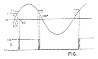
- the flip-flop will switch at 22 (30 worse case) degrees into the positive cycle (see Figure 1). Since the triggering of the SCR 14, as described below, depends on this timing, the solenoid coil 12 will fire at 22 to 30 degrees into the positive cycle. This effect is considered negligible since less than 5% of the energy is contained in this early portion of the cycle.
- the Q/ output waveform may exhibit double switching between set and reset (a "glitch") near the time when the flip-flop sets or resets.
- Capacitor C2 prevents such "glitches”.
- the second flip-flop (FF2) is used as a clocked flip-flop in order to set at the beginning (or within 30 o of the beginning) of the positive cycle of the AC voltage. FF2, however, will not change state unless switch S1 is closed. With S1 open, the D input of FF2 remains low and the flip-flop will remain reset.
- the flip-flop will trigger if the D input happens to be high during the positive transition of the waveform into the Clock input. If the next positive transition of this waveform occurs when the D input is low, the flip-flop will reset.
- the resetting of FF2 is undesirable because eventually the D input will go high again and there will be two positive transitions into C3 thus causing the SCR to fire on two successive positive cycles of the AC input. In order for this to occur, the contact bounce on the switch must last for at least the duration of one cycle of the AC input.
- the same analysis applies to the opening of the switch S1 in which case the D input goes from high to low.
- the circuit thus provides inherent switch bounce rejection equal to one cycle of the AC input (16.6 milliseconds for 60 Hz and 20 milliseconds for 50 Hz).
- Capacitor C4 reduces high frequency noise pick-up in the leads to the switch. This noise can cause firing of the circuit when the AC power is applied to the circuit or when AC line transients are present.
- capacitor C5 The purpose of capacitor C5 is to prevent firing of the SCR due to AC line noise.
- This noise which can consist of spikes of voltage of up to 2000 volts in amplitude and rise time of several microseconds, can exceed the dv/dt noise rejection of the SCR.
- C5 reduces the magnitude of dv/dt across the SCR.
Landscapes
- Electronic Switches (AREA)
Abstract
Description
- The present invention relates to drive circuits in general and, more particularly, to a drive circuit that is responsive to an input AC voltage for providing a switch actuated drive signal to a load circuit such as, a solenoid coil without the deleterious effect of switch contact bounce.
- Various drive circuits for actuating electrically operated stapling devices have been disclosed in the art. For example, U. S. Patent No. 4,333,019 and U. S. Patent No. 4,492,880 disclose such circuits. Drive circuits for electric staplers and the like should provide a high degree of immunity from false actuations that can be produced by noise and other pulses in the AC line voltage. In addition, such drive circuits should prevent accidental firings that may result from switch bounce and other artifacts.
- It is accordingly a general object of the present invention to provide an improved driver circuit.
- It is a specific object of the invention to provide an improved driver circuit for use with an electric stapler.
- It is a further object of the invention to provide a driver circuit that is responsive to an input AC voltage to generate a drive signal for a load circuit, such as, a solenoid coil in response to the actuation of a switch.
- It is another object of the invention to provide a driver circuit that is independent of the frequency of the input AC voltage.
- It is still another object of the invention to provide a driver circuit that provides switch bounce rejection for one full cycle of the input AC voltage.
- This application is a continuation-in-part application of Serial No. 228,291, filed August 4, 1988 by Harold Weiss and Edward I. Parker for Solenoid Drive Circuit.
- The driver circuit of the present invention is responsive to an input AC voltage to provide a drive signal to a load circuit, such as, a solenoid coil for each actuation of a switch. The input AC voltage sine wave is shaped to produce a positive edge delayed square wave timing signal. The timing signal is applied to a continuously clocked flip-flop which generates a control signal for a selected period of time upon actuation. The control signal is related to one cycle of the AC input voltage. The selected period of time occurs only during the positive portion of the input AC voltage cycle. The control signal from the continuously clocked flip-flop is employed to actuate a firing circuit that supplies the actual drive signal to the load circuit. Switch bounce rejection occurs for a period equal to one full period of the AC input voltage.
- The above objects and other objects and features and advantages of the present invention will become apparent from a detailed description of a preferred embodiment of the invention, selected for purposes of illustration and shown in the accompanying drawings, in which:
- FIG. 1 is a wave form diagram showing the AC input voltage wave plotted against the Q/output of the first flip-flop;
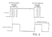
- FIG. 2 is a wave form diagram showing the effect of switch bounce; and,
- FIG. 3 is a schematic diagram of the driver circuit of the present invention.
- Referring now the drawings and particularly to the schematic of FIG. 3, there is shown a driver circuit of the present invention indicated generally by the
reference numeral 10 for providing a drive signal to aload circuit 12, such as, the coil of an electric stapler. - The
soleonid driver circuit 10 is capable of triggering anSCR 14 for a single half-cycle of the AC line. The circuit comprises apower supply section 16, asine wave shaper 18, a clocked flip-flop 20, anSCR coupling 22 and theSCR 14. - The power supply section is used to generate VDD (drain voltage) for a dual D flip-flop, FF₁ and FF₂ such as, a
CMOS 4013B. A source of input AC voltage (not shown) is applied to drivercircuit input terminals voltage divider 28 and a half-wave rectifier 30. Thevoltage divider 28 uses resistors R₁ and R₂. The rectifier circuit with a filter capacitor C₁ generates an output of 12 volts DC with a ripple of +/-2 volts at nominal AC line input (115 volts). - The
sine wave shaper 18 is used to decrease the rise and fall time of the AC input waveform in order to insure a fast transition through the switching region of the clocked flip-flop. The first stage (FF₁) of the dual flip-flop is used for this purpose. The AC input voltage, which is passed through thevoltage divider 28, is used as the input to thewave shaper 18. Diode CR₂ is used to prevent the AC voltage from going negative and causing damage to the flip-flop FF₁. - The flip-flop FF₁ has its clock input disabled and is used as an R-S flip-flop. Since the S input is connected to VDD, the output Q/ will be low as long as R is kept low. When R is forced high (during the positive portion of the AC input), the Q/output will be forced high (the Q output will also be high since the S input is held high). The output Q/ will therefore follow the AC input except for the positive edge delay described below.
- The R input of the flip-flop will be considered high if its voltage is 70% of VDD in the worse case, typically if it is 55% of VDD. For 115 VAC input, the peak values at the output of the divider is 14 volts and VDD is 10 volts just prior to the positive peak of the AC input. Thus, when the R input to the flip-flop is 5.5 volts (7 volts worse case), the Q/ output will go high. This corresponds to .39 (.5 worse case) of the peak voltage of 14. Thus, the flip-flop will switch at 22 (30 worse case) degrees into the positive cycle (see Figure 1). Since the triggering of the
SCR 14, as described below, depends on this timing, thesolenoid coil 12 will fire at 22 to 30 degrees into the positive cycle. This effect is considered negligible since less than 5% of the energy is contained in this early portion of the cycle. - Due to the slow rise and fall times of the signal at the Reset input, the Q/ output waveform may exhibit double switching between set and reset (a "glitch") near the time when the flip-flop sets or resets. Capacitor C₂ prevents such "glitches".
- The second flip-flop (FF₂) is used as a clocked flip-flop in order to set at the beginning (or within 30o of the beginning) of the positive cycle of the AC voltage. FF₂, however, will not change state unless switch S₁ is closed. With S₁ open, the D input of FF₂ remains low and the flip-flop will remain reset.
- When S₁ is closed, the D input of FF₂ will go high and the next positive edge of the timing signal from FF₁ will set FF₂. When FF₂ is set, the Q output will switch from low to high thereby generating a positive pulse through C₃ and triggering the SCR.
- The closing of switch S₁ does not generate a single step function from low to high at the D input because the switch is subject to contact bounce. Figure 2 shows the waveform at the D of FF₂ input when the effect of switch bounce is considered.
- The flip-flop will trigger if the D input happens to be high during the positive transition of the waveform into the Clock input. If the next positive transition of this waveform occurs when the D input is low, the flip-flop will reset. The resetting of FF₂ is undesirable because eventually the D input will go high again and there will be two positive transitions into C₃ thus causing the SCR to fire on two successive positive cycles of the AC input. In order for this to occur, the contact bounce on the switch must last for at least the duration of one cycle of the AC input. The same analysis applies to the opening of the switch S₁ in which case the D input goes from high to low. The circuit thus provides inherent switch bounce rejection equal to one cycle of the AC input (16.6 milliseconds for 60 Hz and 20 milliseconds for 50 Hz).
- Capacitor C₄ reduces high frequency noise pick-up in the leads to the switch. This noise can cause firing of the circuit when the AC power is applied to the circuit or when AC line transients are present.
- The purpose of capacitor C₅ is to prevent firing of the SCR due to AC line noise. This noise, which can consist of spikes of voltage of up to 2000 volts in amplitude and rise time of several microseconds, can exceed the dv/dt noise rejection of the SCR. C₅ reduces the magnitude of dv/dt across the SCR.
- By way of illustration only, the following parts list can be employed in constructing the driver circuit shown in Figure 3.
-
- R₁ Resistor, carbon, 33K ohms, 1/2 watt, 5% (115 volts)
Resistor, carbon, 68K ohms, 1 watt,5% (230 volts) - R₂ Resistor, carbon, 3.9K ohms, 1/4 watt, 5%
- R₃ Resistor, carbon, 100K ohms, 1/4 watt, 5%
- C₁ Capacitor, aluminum electrolytic, radial leads, 2,2 Mfd., +/-20%, 25 volts
- C₂,C₄, C₅ Capacitor, ceramic disc, .0047 Mfd., +/-20%, 500 volts
- C₃ Capacitor, ceramic disc, .047 Mfd., +/20%, 25 volts
- CR₁ Diode, 1N4148
- CR₂
- U₁ D-Type Dual Flip-Flop, CMOS, 4013B:
Fairchild F4013BC
Motorola MC1403BCP
National CD4013BC
Panasonic MN4013B
RCA 4013B
Signetics HEF4013BP
SSS SCL4013BE - SCR₁ Silicon Controlled Rectifier:
RCA S2800D,E,M (400, 500, 600 VDRM)
TAG S1007M - Having described in detail a preferred embodiment of our invention, it will now be apparent to those skilled in the art that numerous modifications can be made therein without departing from the scope of the invention as defined in the following claims.
Claims (11)
Applications Claiming Priority (4)
| Application Number | Priority Date | Filing Date | Title |
|---|---|---|---|
| US22829188A | 1988-08-04 | 1988-08-04 | |
| US32543889A | 1989-03-20 | 1989-03-20 | |
| US325438 | 1989-03-20 | ||
| US228291 | 1994-04-15 |
Publications (2)
| Publication Number | Publication Date |
|---|---|
| EP0353765A2 true EP0353765A2 (en) | 1990-02-07 |
| EP0353765A3 EP0353765A3 (en) | 1991-03-27 |
Family
ID=26922231
Family Applications (1)
| Application Number | Title | Priority Date | Filing Date |
|---|---|---|---|
| EP19890114400 Ceased EP0353765A3 (en) | 1988-08-04 | 1989-08-03 | Solenoid drive circuit |
Country Status (1)
| Country | Link |
|---|---|
| EP (1) | EP0353765A3 (en) |
Cited By (1)
| Publication number | Priority date | Publication date | Assignee | Title |
|---|---|---|---|---|
| EP0590687A1 (en) * | 1992-10-02 | 1994-04-06 | Eastman Kodak Company | Apparatus and technique for connecting a source of zero crossing AC voltage to and disconnecting it from an AC load line |
Family Cites Families (2)
| Publication number | Priority date | Publication date | Assignee | Title |
|---|---|---|---|---|
| US4370564A (en) * | 1980-06-04 | 1983-01-25 | Ricoh Company, Ltd. | AC Switching device |
| DE3216928A1 (en) * | 1982-05-06 | 1983-11-10 | Pütz, Willi, 6277 Camberg | Contact-controlled switch |
-
1989
- 1989-08-03 EP EP19890114400 patent/EP0353765A3/en not_active Ceased
Cited By (2)
| Publication number | Priority date | Publication date | Assignee | Title |
|---|---|---|---|---|
| EP0590687A1 (en) * | 1992-10-02 | 1994-04-06 | Eastman Kodak Company | Apparatus and technique for connecting a source of zero crossing AC voltage to and disconnecting it from an AC load line |
| US5410193A (en) * | 1992-10-02 | 1995-04-25 | Eastman Kodak Company | Apparatus and technique for connecting a source of zero crossing AC voltage to and disconnecting it from an AC load line |
Also Published As
| Publication number | Publication date |
|---|---|
| EP0353765A3 (en) | 1991-03-27 |
Similar Documents
| Publication | Publication Date | Title |
|---|---|---|
| KR940007080B1 (en) | Load control system | |
| US5804991A (en) | Zero crossing circuit for a relay | |
| AU709315B2 (en) | Triac control circuit | |
| US4725769A (en) | Current limited for constant current for switching driving devices | |
| US4394583A (en) | Electric fence energizers | |
| MXPA06014428A (en) | Apparatus and methods for regulating delivery of electrical energy. | |
| US4163923A (en) | Variable duty cycle lamp circuit | |
| NL8201481A (en) | SYSTEM FOR ELECTRICAL POWERING AND SWITCHING OF A NUMBER OF POWER-USING APPLIANCES. | |
| US4270058A (en) | Power supply and control circuit for series connected controller | |
| US4443709A (en) | Frequency responsive system power sequencer | |
| US6249417B1 (en) | Electrical circuit for producing a substantially constant pulsed magnetic field for repelling rodents | |
| EP0152414B1 (en) | A driver circuit | |
| US5144520A (en) | Power solenoid drive circuit with switch bounce rejection | |
| US4260947A (en) | Phase control circuit for regulating power | |
| US5146388A (en) | Variable power drive circuit | |
| EP0590687A1 (en) | Apparatus and technique for connecting a source of zero crossing AC voltage to and disconnecting it from an AC load line | |
| JPH04109862A (en) | Dynamic ignition method and control circuit for multiple triacs | |
| US4333019A (en) | Silicon controlled rectifier trigger circuit | |
| US3648076A (en) | Capacitance-responsive control system | |
| GB1592971A (en) | Electrical appliance control | |
| US4034240A (en) | Sine-to-square wave converter | |
| US5565750A (en) | Apparatus for applying field excitation to a synchronous electric motor | |
| JPH0569285B2 (en) | ||
| US4926062A (en) | Touch control circuit for ornamental lamps and method therefore | |
| US4223195A (en) | Pulse transformer |
Legal Events
| Date | Code | Title | Description |
|---|---|---|---|
| PUAI | Public reference made under article 153(3) epc to a published international application that has entered the european phase |
Free format text: ORIGINAL CODE: 0009012 |
|
| AK | Designated contracting states |
Kind code of ref document: A2 Designated state(s): AT BE CH DE ES FR GB GR IT LI LU NL SE |
|
| PUAL | Search report despatched |
Free format text: ORIGINAL CODE: 0009013 |
|
| AK | Designated contracting states |
Kind code of ref document: A3 Designated state(s): AT BE CH DE ES FR GB GR IT LI LU NL SE |
|
| 17P | Request for examination filed |
Effective date: 19910911 |
|
| RAP1 | Party data changed (applicant data changed or rights of an application transferred) |
Owner name: STANLEY-PARKER, INC. |
|
| 17Q | First examination report despatched |
Effective date: 19940428 |
|
| STAA | Information on the status of an ep patent application or granted ep patent |
Free format text: STATUS: THE APPLICATION HAS BEEN REFUSED |
|
| 18R | Application refused |
Effective date: 19960408 |