EP0354462A2 - Agencement de circuit pour détecteurs d'infrarouge - Google Patents
Agencement de circuit pour détecteurs d'infrarouge Download PDFInfo
- Publication number
- EP0354462A2 EP0354462A2 EP89114285A EP89114285A EP0354462A2 EP 0354462 A2 EP0354462 A2 EP 0354462A2 EP 89114285 A EP89114285 A EP 89114285A EP 89114285 A EP89114285 A EP 89114285A EP 0354462 A2 EP0354462 A2 EP 0354462A2
- Authority
- EP
- European Patent Office
- Prior art keywords
- circuit arrangement
- circuit
- arrangement according
- transistor
- capacitor
- Prior art date
- Legal status (The legal status is an assumption and is not a legal conclusion. Google has not performed a legal analysis and makes no representation as to the accuracy of the status listed.)
- Granted
Links
Images



Classifications
-
- G—PHYSICS
- G01—MEASURING; TESTING
- G01J—MEASUREMENT OF INTENSITY, VELOCITY, SPECTRAL CONTENT, POLARISATION, PHASE OR PULSE CHARACTERISTICS OF INFRARED, VISIBLE OR ULTRAVIOLET LIGHT; COLORIMETRY; RADIATION PYROMETRY
- G01J5/00—Radiation pyrometry, e.g. infrared or optical thermometry
- G01J5/10—Radiation pyrometry, e.g. infrared or optical thermometry using electric radiation detectors
- G01J5/28—Radiation pyrometry, e.g. infrared or optical thermometry using electric radiation detectors using photoemissive or photovoltaic cells
- G01J5/30—Electrical features thereof
-
- H—ELECTRICITY
- H04—ELECTRIC COMMUNICATION TECHNIQUE
- H04N—PICTORIAL COMMUNICATION, e.g. TELEVISION
- H04N25/00—Circuitry of solid-state image sensors [SSIS]; Control thereof
- H04N25/20—Circuitry of solid-state image sensors [SSIS]; Control thereof for transforming only infrared radiation into image signals
- H04N25/21—Circuitry of solid-state image sensors [SSIS]; Control thereof for transforming only infrared radiation into image signals for transforming thermal infrared radiation into image signals
Definitions
- the invention relates to a circuit arrangement for infrared detectors, in particular for thermal imaging devices with photoresistors as detector elements.
- Highly sensitive devices for detecting infrared radiation have a detector which consists of many independent detector elements.
- the maximum number of detector elements is limited to approximately 300 in the wavelength range around 10 ⁇ m. Therefore the image has to be scanned optically.
- the wavelength range around 4 ⁇ m there are detectors with 250,000 detector elements. The quantum efficiency of these detectors is so bad, however, that the image is scanned with a much smaller number of detector elements in this area for highly sensitive devices.
- detectors with electronic scanning methods based on the CCD principle are not available for the infrared ranges mentioned above.
- a preamplifier and a post-amplifier are therefore assigned to each detector element.
- the effort for the amplifiers is very large. 288 preamplifiers and 288 post amplifiers are required. In addition, the amplifiers are capacitively coupled, so that a large number of coupling capacitors are added.
- the capacitance of the coupling capacitors is relatively large because the scan frequency is only 50 Hz. Therefore, a compromise is often made and the coupling capacitors are dimensioned too small, which then leads to undesirable roof slopes in the signal.
- the object of the invention is to provide a circuit arrangement of the type mentioned at the outset with which the disadvantages mentioned above are avoided.
- the circuit arrangement according to the invention is simple in construction and accordingly takes up a small installation space. It provides a good signal-to-noise ratio.
- the circuit arrangement does not require coupling capacitors.
- This property is particularly important when tracking fast moving objects. It is necessary for a large dynamic range of the circuit arrangement according to the invention and for the use of the full circuit sensitivity under all observation conditions; eg if the full amplification is nevertheless set in a high-contrast scene in order to recognize an object with low local contrast, the temperatures of the Object deviate greatly from the mean temperature of the scene.
- the above-mentioned clamping also has the task of regulating the resulting offset voltages of the amplifiers to zero.
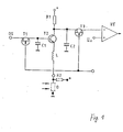
- Figure 1 shows a circuit arrangement according to the invention in an exemplary embodiment.
- One of the 288 detectors D is in series with an inductance L in the emitter line of a transistor T2, at the base of which there are an electronic switch T1 and a capacitor C1 as part of a voltage control loop.
- a control voltage OS is supplied to the electronic switch T1.
- the collector direct current for transistor T2 is supplied via a resistor R1.
- At the input M there is a control voltage for controlling the electronic switches T1 and T3.
- the transistor T2 amplifies the signal voltage of the detector D.
- the time constant (R1. C2) is greater than one sampling period between two successive detectors. Therefore, the circuit arrangement works as an integrator for the photo current supplied by the detector D.
- the signal current stored in the capacitor C2 during a sampling period is discharged to the reference voltage U0 during the short sampling time ( ⁇ 40 ns) via the electronic switch T3 (multiplexer).
- the input stage of the amplifier VE has an active input resistor, which accelerates the charge transfer. Only one common VE amplifier is required for all 288 channels.
- the average direct current for the transistor T2 is supplied via the resistor R1, so that only the signal currents flow via the switch T3.
- FIG. 2 shows the relative frequency response of capacitor C2 together with switch T3. The influence of inductance L is therefore not taken into account.
- the frequency normalized to the column scanning frequency f ⁇ is plotted on the horizontal axis.
- the maximum signal frequency f omax which contains optical information, is 26.25 kHz. This frequency is also entered in FIG. 2.
- the detector D is arranged in the emitter line of the transistor T2.
- This arrangement has the advantage that the tolerances of quantum efficiency and resistance of the detector element do not add up.
- the differences in the signals at the output of the individual 288 preamplifier channels are therefore smaller than with the conventional basic control.
- the power gain of the basic circuit is lower than that of an emitter circuit, it is sufficient.
- the circuit has the advantage that the effective external resistance in the base circuit is almost zero. Accordingly, the base current sparkle noise is very low in contrast to circuits with coupling capacitors in the base circuit, because there the impedance of the coupling capacitors rises sharply at very low frequencies.
- the MESFET T3 working as a multiplexer, switches the signal to the common output for all preamplifier channels.
- GaAs-FETs are used as switches because they enable very short switching times, low switch-on resistances, low switching interference voltages and very low crosstalk between the input and output. Nevertheless, the switching interference is not negligible compared to the smallest signal. However, these residual disturbances only act like an offset voltage of the amplifiers and are therefore rendered ineffective by an offset voltage control loop according to the invention.
- the components T1, C1 belong to the offset voltage control loop.
- the field effect transistor T1 which can also be a bipolar transistor, switches the control voltage OS briefly to the capacitor C1. This capacitor stores the information until the next switching.
- the offset voltage regulator adjusts the voltage OS until the voltage U0 is at the collector of the transistor T2 at the time when the clamping surface is scanned.
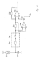
- the recharging of the capacitor C1 can be accelerated by an external, active circuit - which is common to all 288 channels - for example the circuit according to FIG. 4, 5 or 6.
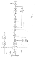
- Fig. 3 shows the block diagram of the analog signal processing, e.g. for a thermal imaging device.
- the elements to the left of the dashed line are each assigned to a detector element, so they are needed 288 times. In contrast, in the section to the right of this, the signals from all 288 detector elements are processed sequentially. Accordingly, the functional elements of this section are only required once.
- the elements to the left of the dashed line contain the circuit arrangement according to the invention, e.g. 1 or 7.
- the essential parts of this circuit arrangement are named here with the corresponding reference numerals in FIG.
- the amplifier VV referred to as the preamplifier, is formed in cooperation with the multiplexer T3 by the transistor T2, the resistor R1, the inductor L and the capacitor C2.
- the output of the multiplexer T3 controls the discharge amplifier VE, which converts the charge stored in the capacitors of the preamplifiers and proportional to the detector signal into a voltage. In addition, the charge of these capacitors must be reset to a defined value by this amplifier. This is followed by actuator SG1, which controls the individual gain of the 288 channels.
- the signal H coming from the brightness controller is added.
- the sign of the brightness signal is such that the amplitude of the signal to be processed is brought close to the amplitude of the signal that is present when the clamping surface is scanned. This is necessary because the signal background, which is largely eliminated by this measure, is several powers of ten greater than may be the smallest detectable signal. As a result, the subsequent stages are subject to only minor requirements with regard to the large signal behavior.
- the electronic switch S2 closes while the image is being scanned. It is open when the clamping surfaces are scanned and during the scanner return.
- the following amplifiers V1, V2, V3 are very broadband (100 MHz). It is particularly important that their recovery time after an overload is much shorter than the signal duration for one pixel. This is necessary because, with large intensifications when viewing high-contrast images, clipping in uninteresting parts of the image is inevitable. The short recovery times now guarantee that no tracing occurs after the overdriven image sections.
- the amplifier V1 in particular is also very low-noise because the noise bandwidth of the common channel is greater by a factor of 300 than that of the amplifier.
- the amplification can be set with the actuators SG2, SG3.
- a contrast signal K is fed in.
- the filter F1 limits the bandwidth to the bandwidth of ⁇ 25 MHz that is absolutely necessary for the multiplex transmission. This is necessary so that the amplitude of the noise behind the multiplexer can be neglected compared to the noise from the detector.
- the noise generated in the common channel is considerably broadband than the preamplifier noise, but without a low-pass filter it would be irreversibly reflected in the useful signal range on the non-linear characteristic of limiter B.
- the limiter B delivers a signal amplitude at the output which is adapted to the modulation range of the A / D converter. In this way, the overloading of the A / D converter is avoided.
- the recovery time of the A / D converter is greater than that of limiter B. Without limiter B, crosstalk between adjacent signals could occur, which must be avoided in particular because, due to the interlacing method and the selected column scanning method, signals that are adjacent in time are not spatially correspond to neighboring pixels.
- the amplifier V4 drives the A / D converter.
- the control signal OS of the offset voltage control loop sets the voltage at the output of the amplifier V4 - while the clamping surfaces are scanned - to a predetermined reference level.
- Another control loop according to the invention via the components S4, V6 ensures an offset voltage adjustment of the amplifier chain V2 to V4: this control loop works during the return time of the scanner.
- switch S3 is opened and S4 closed during this time;
- the offset according to the invention is used here voltage control loop described again coherently.
- This offset voltage control loop enables DC voltage coupling from the detector to the output of the main amplifier by regulating the resulting offset voltage to zero.
- this controller takes over the task that the clamping circuit otherwise has.
- the optical reference surface to the left of the image to be scanned is used as a reference radiator for the offset control loop.
- a corresponding surface which is about 10 K warmer relative to the left surface.
- the temperature can be adjusted to the temperature window set by heating or cooling.
- This area is the radiation reference area for the control loop, which is the compensates for different sensitivities of the individual detector elements by influencing the transmission factor of the actuator SG1.
- the system controller calculates the manipulated variables and controls the corresponding D / A converter.
- the amplitudes of the individual channels at the output of the actuator SG1 when the radiation reference surface is scanned are all of the same size. So that the reference signal has the optimal size, the gain of the main amplifier is briefly changed during this time, by intervention in the control signal K for the actuators SG2, SG3. (The main amplifier is the amplifier circuit from amplifier VE to V4).
- the resistor R1 in FIG. 1 can be replaced by a current source.
- other components acting as switches can be used for the electronic switches T1, T3 in FIG. 1.
- the arrangement of the detector D in the emitter circuit offers advantages. In principle, however, the detector can also be inserted in the base circle, as shown in FIG. 7. However, more components are required if the offset control voltage OS is also to be supplied to the base.
- the electronic switches T1, T3 in FIG. 1 can be made conductive at different times.
- the resistor R1 in FIG. 1 or the equivalent current source can also be completely dispensed with.
- the charge loss of the capacitor C2 through the direct current of the transistor T2 is then briefly (briefly in Comparison to the sampling period) replaced by an electronic switch, as shown in FIG. 7. In principle, this can be done via the electronic switch T3.
- the amount of charge for the charge equalization for the transistor direct current can be regulated with the aid of the offset voltage regulator described above. In this case, the sample and hold circuit T1, C1 in the base circuit of the transistor T2 can be omitted.
- R11 is the unwanted resistance of the electronic switch when the switch is on.
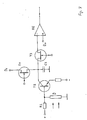
- Fig. 4 shows such an active rapid recharge circuit.
- the collector current of the transistor T2 or its base current and other leakage currents are symbolized here by the current source Q11.
- the capacitor C11 to be recharged (corresponding to C2 in FIG. 1) is discharged via the electronic switch S11 with the internal resistor R11.
- the discharge current causes a voltage drop across the resistor R12. This voltage drop is after the sign reversal in the amplifier V11 at the input of the amplifier V12.
- the sign of this feedback is chosen so that the amplifier applies a voltage to the electronic switch via the resistors R13, R12, which increases the charge-reversal current.
- the negative internal resistance of the recharging circuit can be set by selecting the resistors R12, R13. However, due to the inevitable tolerances, the resulting discharge resistance can practically only be reduced by a factor of 10.
- the voltage to which the capacitor C11 is recharged is specified by the reference voltage U0, A11 is a summing stage.
- a rapid recharging circuit according to the invention with which the resulting discharge resistance can be reduced by more than a factor of 50 even with very short recharging times, is shown in FIG U0 determined and corresponding to this difference by means of the amplifier V13 to the electronic switch S11, via which the charge-reversal current flows, a voltage is applied which increases the charge-reversal current.
Landscapes
- Engineering & Computer Science (AREA)
- Multimedia (AREA)
- Signal Processing (AREA)
- Physics & Mathematics (AREA)
- General Physics & Mathematics (AREA)
- Spectroscopy & Molecular Physics (AREA)
- Transforming Light Signals Into Electric Signals (AREA)
- Amplifiers (AREA)
- Photometry And Measurement Of Optical Pulse Characteristics (AREA)
Applications Claiming Priority (2)
| Application Number | Priority Date | Filing Date | Title |
|---|---|---|---|
| DE3827465A DE3827465A1 (de) | 1988-08-12 | 1988-08-12 | Verstaerker fuer infrarotdetektoren |
| DE3827465 | 1988-08-12 |
Publications (3)
| Publication Number | Publication Date |
|---|---|
| EP0354462A2 true EP0354462A2 (fr) | 1990-02-14 |
| EP0354462A3 EP0354462A3 (fr) | 1991-07-10 |
| EP0354462B1 EP0354462B1 (fr) | 1995-04-05 |
Family
ID=6360765
Family Applications (1)
| Application Number | Title | Priority Date | Filing Date |
|---|---|---|---|
| EP89114285A Expired - Lifetime EP0354462B1 (fr) | 1988-08-12 | 1989-08-02 | Agencement de circuit pour détecteurs d'infrarouge |
Country Status (3)
| Country | Link |
|---|---|
| US (1) | US5038026A (fr) |
| EP (1) | EP0354462B1 (fr) |
| DE (2) | DE3827465A1 (fr) |
Families Citing this family (3)
| Publication number | Priority date | Publication date | Assignee | Title |
|---|---|---|---|---|
| US5196703A (en) * | 1991-09-27 | 1993-03-23 | Texas Instruments Incorporated | Readout system and process for IR detector arrays |
| US5442176A (en) * | 1993-10-06 | 1995-08-15 | Raytheon Company | Infrared detector array |
| FR2844129B1 (fr) * | 2002-09-03 | 2004-10-29 | Suisse Electronique Microtech | Procede et capteur pour determiner le contraste local d'une scene observee, par detection de la luminance emanant de cette scene |
Family Cites Families (9)
| Publication number | Priority date | Publication date | Assignee | Title |
|---|---|---|---|---|
| US4173723A (en) * | 1978-01-12 | 1979-11-06 | Rockwell International Corporation | Photo detector input circuit |
| US4567363A (en) * | 1983-06-20 | 1986-01-28 | Santa Barbara Research Center | Switched capacitor transresistance amplifier |
| US4733077A (en) * | 1984-12-20 | 1988-03-22 | Hughes Aircraft Company | Noise immune infrared readout circuitry |
| US4659928A (en) * | 1985-04-22 | 1987-04-21 | Texas Instruments Incorporated | Focal plane array infrared device |
| US4775798A (en) * | 1985-05-30 | 1988-10-04 | Thomson-Csf | Device for detection with time delay and phase integration |
| GB2181010B (en) * | 1985-09-20 | 1989-09-06 | Philips Electronic Associated | Infrared imaging devices |
| DE3615925A1 (de) * | 1986-05-12 | 1987-11-19 | Hughes Aircraft Co | Integrierender kapazitiv gekoppelter transimpedanzverstaerker |
| US4791286A (en) * | 1987-04-27 | 1988-12-13 | Irvine Sensors Corporation | Pre-amplifier in focal plane detector array |
| US4868902A (en) * | 1988-02-03 | 1989-09-19 | Hughes Aircraft Company | GaAs capacitive feedback transimpedance amplifier |
-
1988
- 1988-08-12 DE DE3827465A patent/DE3827465A1/de not_active Withdrawn
-
1989
- 1989-08-02 EP EP89114285A patent/EP0354462B1/fr not_active Expired - Lifetime
- 1989-08-02 DE DE58909154T patent/DE58909154D1/de not_active Expired - Fee Related
- 1989-08-04 US US07/389,684 patent/US5038026A/en not_active Expired - Lifetime
Also Published As
| Publication number | Publication date |
|---|---|
| DE3827465A1 (de) | 1990-02-15 |
| DE58909154D1 (de) | 1995-05-11 |
| EP0354462B1 (fr) | 1995-04-05 |
| EP0354462A3 (fr) | 1991-07-10 |
| US5038026A (en) | 1991-08-06 |
Similar Documents
| Publication | Publication Date | Title |
|---|---|---|
| DE3432229C2 (de) | Bildaufnahmevorrichtung | |
| DE19809727C2 (de) | Endoskopsystem mit Fluoreszenzlicht | |
| DE69327986T2 (de) | System zur automatischen Kompensation der Kabeldämpfung | |
| DE69221054T2 (de) | Lese-System und Verfahren für Infrarotdetektoranordnungen | |
| DE2845816C2 (de) | Schaltung zur Kontrasterhöhung eines Videosignales | |
| DE3913803A1 (de) | Belichtungsregeleinrichtung | |
| DE2029627C3 (de) | Kompensationsschaltung für eine optische Abtasteinrichtung | |
| EP0848882A1 (fr) | Dispositif de detection de lumiere a courant de decalage programmable | |
| EP0354462B1 (fr) | Agencement de circuit pour détecteurs d'infrarouge | |
| DE2700274A1 (de) | Stromversorgungseinrichtung fuer bildverstaerker | |
| DE2801495C3 (de) | Vorrichtung zur Erzeugung eines oder mehrerer Bildsignale, die eine Information über die Bildschärfe eines Bildes oder über die Lagedifferenz zwischen zwei Bildern enthalten | |
| EP0510408B1 (fr) | Agencement de photodétecteur | |
| DE10125307A1 (de) | Optischer Sensor | |
| DE2037997A1 (de) | Infrarotthermograph mit automatischer Helligkeitssteuerung | |
| DE2208344A1 (de) | Anordnung mit mehreren Strahlungsfühlern | |
| DE2501653C3 (de) | Schaltungsanordnung zum logarithmischen Verstärken | |
| WO2002032114A1 (fr) | Capteur optique | |
| DE3147567C2 (de) | Belichtungssteuerung für eine Kamera | |
| DE3339195C2 (fr) | ||
| DE60133195T2 (de) | Signalverarbeitung für photoleitende Detektoren | |
| DE4343072C1 (de) | Röntgendiagnostikeinrichtung | |
| DE3615925A1 (de) | Integrierender kapazitiv gekoppelter transimpedanzverstaerker | |
| DE69215943T2 (de) | Verarbeitungsschaltung mit Integrator und Tiefpassfilter für jeden Pixel einer infraroten Bildebene-Matrix | |
| DE2526375C3 (de) | Verfahren und Schaltungsanordnung zur Gleichmachung der Verstärkung von mehreren wechselspannungsgekoppelten Video-Detektorverstärkerkanälen eines Überwachungssystems | |
| DE2853456A1 (de) | Steuerschaltung fuer eine bildaufnahmeroehre |
Legal Events
| Date | Code | Title | Description |
|---|---|---|---|
| PUAI | Public reference made under article 153(3) epc to a published international application that has entered the european phase |
Free format text: ORIGINAL CODE: 0009012 |
|
| AK | Designated contracting states |
Kind code of ref document: A2 Designated state(s): DE FR GB IT NL |
|
| PUAL | Search report despatched |
Free format text: ORIGINAL CODE: 0009013 |
|
| AK | Designated contracting states |
Kind code of ref document: A3 Designated state(s): DE FR GB IT NL |
|
| 17P | Request for examination filed |
Effective date: 19920110 |
|
| 17Q | First examination report despatched |
Effective date: 19931019 |
|
| ITF | It: translation for a ep patent filed | ||
| GRAA | (expected) grant |
Free format text: ORIGINAL CODE: 0009210 |
|
| AK | Designated contracting states |
Kind code of ref document: B1 Designated state(s): DE FR GB IT NL |
|
| GBT | Gb: translation of ep patent filed (gb section 77(6)(a)/1977) |
Effective date: 19950403 |
|
| REF | Corresponds to: |
Ref document number: 58909154 Country of ref document: DE Date of ref document: 19950511 |
|
| ET | Fr: translation filed | ||
| PLBE | No opposition filed within time limit |
Free format text: ORIGINAL CODE: 0009261 |
|
| STAA | Information on the status of an ep patent application or granted ep patent |
Free format text: STATUS: NO OPPOSITION FILED WITHIN TIME LIMIT |
|
| 26N | No opposition filed | ||
| REG | Reference to a national code |
Ref country code: GB Ref legal event code: 732E |
|
| NLS | Nl: assignments of ep-patents |
Owner name: BRITISH AEROSPACE PUBLIC LIMITED COMPANY |
|
| REG | Reference to a national code |
Ref country code: FR Ref legal event code: TP |
|
| PGFP | Annual fee paid to national office [announced via postgrant information from national office to epo] |
Ref country code: FR Payment date: 20000807 Year of fee payment: 12 |
|
| PGFP | Annual fee paid to national office [announced via postgrant information from national office to epo] |
Ref country code: GB Payment date: 20000811 Year of fee payment: 12 |
|
| PGFP | Annual fee paid to national office [announced via postgrant information from national office to epo] |
Ref country code: NL Payment date: 20000814 Year of fee payment: 12 |
|
| PGFP | Annual fee paid to national office [announced via postgrant information from national office to epo] |
Ref country code: DE Payment date: 20000823 Year of fee payment: 12 |
|
| PG25 | Lapsed in a contracting state [announced via postgrant information from national office to epo] |
Ref country code: GB Free format text: LAPSE BECAUSE OF NON-PAYMENT OF DUE FEES Effective date: 20010802 |
|
| PG25 | Lapsed in a contracting state [announced via postgrant information from national office to epo] |
Ref country code: NL Free format text: LAPSE BECAUSE OF NON-PAYMENT OF DUE FEES Effective date: 20020301 |
|
| GBPC | Gb: european patent ceased through non-payment of renewal fee |
Effective date: 20010802 |
|
| PG25 | Lapsed in a contracting state [announced via postgrant information from national office to epo] |
Ref country code: FR Free format text: LAPSE BECAUSE OF NON-PAYMENT OF DUE FEES Effective date: 20020430 |
|
| NLV4 | Nl: lapsed or anulled due to non-payment of the annual fee |
Effective date: 20020301 |
|
| PG25 | Lapsed in a contracting state [announced via postgrant information from national office to epo] |
Ref country code: DE Free format text: LAPSE BECAUSE OF NON-PAYMENT OF DUE FEES Effective date: 20020501 |
|
| REG | Reference to a national code |
Ref country code: FR Ref legal event code: ST |
|
| PG25 | Lapsed in a contracting state [announced via postgrant information from national office to epo] |
Ref country code: IT Free format text: LAPSE BECAUSE OF NON-PAYMENT OF DUE FEES;WARNING: LAPSES OF ITALIAN PATENTS WITH EFFECTIVE DATE BEFORE 2007 MAY HAVE OCCURRED AT ANY TIME BEFORE 2007. THE CORRECT EFFECTIVE DATE MAY BE DIFFERENT FROM THE ONE RECORDED. Effective date: 20050802 |