EP0354487A2 - Appareil électronique, numérique, de commutation et/ou de régulation, en particulier interrupteur horaire - Google Patents
Appareil électronique, numérique, de commutation et/ou de régulation, en particulier interrupteur horaire Download PDFInfo
- Publication number
- EP0354487A2 EP0354487A2 EP89114429A EP89114429A EP0354487A2 EP 0354487 A2 EP0354487 A2 EP 0354487A2 EP 89114429 A EP89114429 A EP 89114429A EP 89114429 A EP89114429 A EP 89114429A EP 0354487 A2 EP0354487 A2 EP 0354487A2
- Authority
- EP
- European Patent Office
- Prior art keywords
- input
- switching
- time
- program
- memory
- Prior art date
- Legal status (The legal status is an assumption and is not a legal conclusion. Google has not performed a legal analysis and makes no representation as to the accuracy of the status listed.)
- Granted
Links
Images







Classifications
-
- G—PHYSICS
- G04—HOROLOGY
- G04G—ELECTRONIC TIME-PIECES
- G04G15/00—Time-pieces comprising means to be operated at preselected times or after preselected time intervals
- G04G15/006—Time-pieces comprising means to be operated at preselected times or after preselected time intervals for operating at a number of different times
Definitions
- the invention relates to an operating device and arrangement for an electronic digital switching and / or regulating device, in particular a time switch, optionally with a display device, with at least one first operating element for programming and calling up the stored switching time programs and at least one second operating element for the optional setting of the current current time and the switching times for a selectable structure of the program combination.
- the subject matter of the invention includes assemblies belonging to the device, namely an adjustable clock for the current time, a "summer / winter" time change, the setting of a holiday (pseudo-Sunday) program and one-time duration options - and duration via a definable number of days (vacation program) programmable manual switching, whereby its electronic functions can be controlled or influenced by combined operation and a comparator unit for the outputs of the memory cells with the programmed ON (I) and OFF switching times ( O) in hours (h) and minutes (m) on the one hand and the outputs with the current time of day (h, m) and weekday data (d) on the other.
- an adjustable clock for the current time
- a "summer / winter" time change the setting of a holiday (pseudo-Sunday) program and one-time duration options - and duration via a definable number of days (vacation program) programmable manual switching
- a comparator unit for the outputs of the
- An electronic timer for digital switching and control tasks is known from DE-OS 32 14 372, which has an operating device with a keyboard and therein as operating elements a plurality of pushbuttons, with which all the provided ON and OFF switching times, switching channels, the assigned days of the week, etc. at any time and independently of each other, ie. parallel, and can be set correctable.
- a certain amount of circuitry is of course indispensable for this.
- the effort on operating elements is extremely reduced, for example. in that of the EU patent application 0 197 336 to two, so that the understandably numerous adjustment measures must be carried out in the course of an absolutely necessary repeated repetition of the more or less large number of operations of the operating elements. It is easy to see that this often leads to incorrect settings conditions are unavoidable and repeated, cumbersome corrections must be accepted accordingly.
- the present invention is based on the object, that is to say, in the case of an operating device and arrangement according to the preamble of claim 1, while largely maintaining the ease of use and functionality.
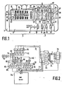
- Fig. 1 for the purpose of comparing the new operating device to that of the prior art of DE-OS 32 14 372, the division of the front panel 2 into an operating and a display field 4 is shown, the total programming operating elements the CLOCK, ON and OFF switching times for the daily range h, m, s, the days of the week, switching channels, with control and function buttons, for the acknowledgment and program saving procedures using the function selection button So ten buttons 15 to 29 in a coded order, 4 function selection buttons "Test", “Check”, “clear” and “reset” Although the high level of convenience of immediate and always accessible, to each data group of a complete data set, ON and OFF switching times with associated information about days of the week, channels, and simultaneous display of the same, but combined with a considerable amount of space and costs. The cost and space requirement of this convenient time program switching device is primarily due to the extensive organization of its control unit.
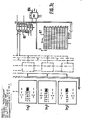
- the circuitry implementation of the comfortable organization of the programming of DE-OS 32 14 372 is shown in a very simplified summary in FIG.
- the generator group 51 feeds via the one branch 52 and the key switches 53, which belong to the operating unit, in the operating mode "set time" 54, the memories 55 for the current current time in the associated buffer.
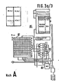
- the concept of the differently disposable partial programs in Fig. 3a is based on actuations of the function selection keys, the setting keys in different serial combinations and in continuous sequence during installation of the program with a specified block of days of the week and in expansion of the respective actuation of the setting buttons in combination with acknowledgment when the switch-on data group is displayed for an ON switching time and then for a switching off time and finally the channel selection, and completion by pressing the function key, with a freely selectable block of days of the week initially for the ON switching time, weekday (s), after a further sequence of actuating and acknowledgment buttons and pressing the function key for OFF switching time and weekday (s) when the OFF switching time group is displayed, the latter with logically correct display of the switch-off days after comparison of the values of the ON switching data with those of the OFF switching data or by additional actuation of the setting key before the acknowledgment after pressing the function key again, and completion by pressing the function key Actuation of the setting and acknowledgment buttons for channel selection, and completion by pressing the function key and returning to
- Each sub-program of the program menu and, if applicable, each of its sub-sections must be closed separately by pressing the function selection key, which enables the input of another sub-program.
- Each of the completely entered partial programs is displayed in succession by repeatedly pressing the function selection key (marked "clock” symbol) as a complete image on the display device until the function selection returns to the first partial memory of the menu. This is displayed when the user program memory is full.
- the programming runs with an alternating sequence of pressing the function key - once at the beginning of a series with the flashing key and the setting key - once or several times - and the acknowledgment key - once - after which the next picture of the menu released for input flashes .
- the starting point of the program menu is indicated by the picture "Monday, midnight” and by empty circles displayed as symbols for "channel”; a colon between the hour and minute display flashes. After pressing the function selection key for the first time, the "clock symbol” appears for the instruction "set time”.
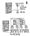
- the column of block diagrams for these cases shows that this possibility is achieved by a step-by-step acknowledgment, either by setting the switch-on time directly together with the days of the week, or by confirming the weekdays for switch-off times automatically set in the section there, by pressing the confirmation button or by Intermediate actuation of the set button ie. the independently programmed selection of the days of the week and the subsequent acknowledgment.
- the column of block diagrams with fixed days of the week shows that the stages of the partial program execution can be processed continuously in one go, composed of alternating sequences of actuating and acknowledgment key actuation.
- This programming in stages also allows simple corrections - repeatable in case of erroneous operation - a few steps to get to the correction point in the program.
- only short jumps are required in order to get from one function block of the partial program to another or from one partial program to another; even without the need for corrections, program jumps can only be made in this way using the function selection key.
- the present new differs from the usual time control by the possibility that by pressing the " ⁇ 1h" key 248 the time control can be shifted from the built-in clock by + 1h, -2h, + 1h etc. This is effected by means of an intermediate time memory 249, the content of which is set additively changed by a shift memory 250.
- the switch to the succeeds in the present case first or at least the second time In contrast to the usual summer-winter switching arrangements, which have the disadvantage that the operator does not know whether to set the time ahead or readjust and therefore have to correct or even re-enter in the worst case, the switch to the succeeds in the present case first or at least the second time.
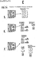
- the holiday (pseudo-Sundays) program represents a technical extension of the program; with the days of the week, which form a kind of short vacation within continuous succession, and the same programs should receive, for example. that of a Sunday, through such days, e.g. Sundays to be replaced.
- the measures necessary in this regard are to be regarded as special hardware features and are dealt with in connection with FIG. 3c.
- these subroutines - as building blocks of the subroutines of the menu program - have a sub-structure in the form of a hierarchy that performs the function of setting the switching times, graduated in counters for the hours and minutes of the ON- Switching time for a channel of the output switch device storing the selected switch-on times in an addressable buffer by actuating an acknowledgment button via an acknowledgment module and finally the function of advancing into a subroutine of essentially the same type or - if the intended number of modules of this type has been processed - Switch to a subsequent stage in the menu by pressing the function selection key.
- the sub-function blocks differ in that they either contain a fixed block (ROM memory) for the days of the week, the advance from module to module automatically to the next position and filing of the ON and OFF switching times, as well as the position and Filing the Channels, takes place, or are freely selectable by means of an intermediate stage.
- the function of setting the days of the week takes place with the help of their continuous addressing in a shift register by means of the setting key, storing those days of the week that are to be adopted by pressing the acknowledgment key in an A-stable block and from there in an addressable weekly memory.
- the operating system for the user program can be optionally assembled from modules, which in the basic level are preferably two counter units in one level, acknowledgment and advance levels in expansion levels, permanent memory units for weekday blocks and finally the variants of the selectable setting one of included multiple channels.
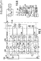
- FIG. 4 shows in a block diagram between the thick lines 101 for the actuating button 102, 103 for the acknowledgment button 104 - input group A for signals of the switch-on time - via the AND gate 105 for the counter 106 (hours) or AND gate 107 for the counter 108 (minutes) can be recognized as the basic stage 109 of the subroutine module 110 with the AND gates 113, 114 connected to outputs 115, 116, respectively.
- An output 115 of the counter block (h) is on the one hand with the input 116 of the AND gate 113 for the buffer 117 (FF) and the output 116 '(counter block m) with the input 118 of the AND gate 114 for the buffer 119 (FF ) connected.
- the output signal 122 of the buffer memory 117 which confirms the transfer of the input into the counter 123, releases the counter 108 for the actuating signal at the second input 126 of the AND gate 107 via the line 124 and the input 125 of the AND gate 107.
- This is followed by the storage of the minute input in the counter 108 and thus via its output 116 'and the input 118 of the AND gate 114 the transfer of the signal to its output - which forms the output of the input group "A" 127 for the switch-on times -
- the output 128 of leads via line 129 to the second input 130 of the AND gate 131 of the input group "B" 132 with the shift register 133 for the position of the days of the week.
- an actuating signal can be entered by actuating the actuating key 102 via the second input 134, each actuation of the actuating key via line 135, the content of the displayed weekday symbol being changed by the actuating pulse a position in the shift register 133 is shifted, or, if the input of the displayed symbol is to be saved, via the line 136 to the input 137 of the AND gate 138 of the acknowledgment group 139 and, when the acknowledgment key (104) is pressed, a takeover command via the second Entrance 140 and the line 141 is fed to the buffer (FF) 142.
- FF buffer
- the signals for the OFF switching times are input via the input group "C" 154 for the OFF switching times, which are equipped with modules in the same way as the input group "A".
- the addresses are derived and stored in the weekday register 147 if the acknowledgment key 104 is actuated and then at these addresses - in accordance with the weekdays for the ON switching data - the weekdays for the OFF switching times in the weekday- Register 147 can be saved.
- the signal at the output of the acknowledgment group 139 can no longer be freely released for the free programming of the weekdays as soon as the acknowledgment key (104) of the acknowledgment group has already been pressed, which results in the output signal of the buffer 166 blocks the NAND gate 164 and the AND gate 165 in the input of the weekday register 147.
- the acknowledgment signal negates 167 the line 162 of the output signal of the buffer memory 166 to the address register 163 of the freely programmed days of the week.
- the weekday registers 143 and 147 with the associated address registers 145, 163 are functionally combined with the ON switching time registers 168 and the OFF switching time register 169 to form the programming memory 170.
- the ON-switching time register 168 is over by the output of the counter output 115 the line 171 in its first pair of job groups (h) 172 and the second job group pair (m) 174 loaded from the counter output 116 via the line 173.
- the OFF switching time register is loaded via line 175 from output 176 of counter 177 of OFF switching time input group 154 for the hours (h) or via line 178 from output 179 of counter 180 of minutes ( m).
- the exemplary embodiment for the functional sub-program "free programming" of the times of day and days of the week is processed by a first actuation of the function selection button, which is indicated symbolically in connection with the AND gate 181, and for the first section of the ON switching times, continued by a second actuation, which is indicated by the AND gate 182, and completed by a third actuation of the function selection button, which is explained in connection with FIG.
- the connection of the function selection button (183) with the block diagram described above is shown by the thick line 184.
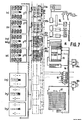
- Fig. 5 - as an extract from the complete program menu of Fig. 3 - is a block diagram of the variant of programming the ON and OFF switching times for selectable switching channels with a fixed block of, for example. reproduced seven days of the week in the manner of the representation of Fig.4.
- the thick lines 101, 103 and 184 to the actuating key (102), acknowledgment key (104) and the function selection key (183) are symbolically entered.
- the latter creates a partial function program or an Ab Cut of it selected, depending on whether the function sub-program can be processed in one go or in several sections, after the processing of which the function selection button must be pressed again, after which the control button can always be pressed to address the selected sub-program .
- the weekday data permanently stored in a ROM memory 201 are stored together with the freely stored ON and OFF switching times and the channel selection data in the programming memory 170 and are linked from there in logical comparator units 202 in order for the Extraction of the ALE link results from the registers assigned to them for the switching devices in the output, together with the relevant signal, to switch the result signals for the switching to the ON or OFF operating state.
- Fig. 5 shows that this principle enables consistent automatic operation by each actuating key actuation indicating the actuating key input or acknowledgment required below and, conversely, each acknowledgment indicating the required subsequent input.
- the circuit logic of each part program is like that of FIG.
- the acknowledgment 210, 211 of the channel selection data leads to another partial program by confirmation by means of the function selection button (183).
- FIG. 6 shows an exemplary embodiment for the time control by means of an electronic clock module 241 known per se with the time cut stages 242 (day of the week “d"), 243 (hours “h") and 244 (minutes “m") designed as counters. with the clock generator 246, consisting of an oscillator 247 and various divider stages, among others for 1 ms, 1/2 s, 1/8 s and 1 s clock signal outputs, e.g. T 1 and T 2, as well as the signals for the ongoing 1 s advancement of the electronic clock module 241.
- the time segment stages 242 to 245 can also be set from the RAM 555 in a manner customary in the industry.
- Two different clock signals are generated by the clock generators 246 via the AND gates 266, 267 released alternately by controlling the second inputs from a time-delayed monostable FLOP element controlled via line 268 to the outputs T 1 and T 2 interchanged after a period of time.
- the time-delayed switchover of the clock signal pushbutton signal input with the setting pushbuttons takes place from individual pulses to a faster sequence of clock pulse series.
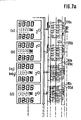
- Fig.3a the special case (2d) is included, in which by installing the partial programs (c2) and (c3) for a more complicated programming two cases, namely for the switching times A OUT Clock five days of the week memory o3.oo 12.oo Clock (Mon-Fri) freely programmable weekday memory 12.oo 16.oo Clock (Mon-Thu) - modularly composed of sub-programs - is realized for a long weekend.
- This example is representative of the multiple usability of the memory organization described, in which the entire program can be assembled in a simple manner using the loop from partial programs of different data, even if from defined formats, that is to say from program modules with overlapping functions.
- the modularity extends to largely any, ie. all data for daily ON and OFF switching data, the weeks subject to change for ON and OFF switching, as well as channels; it is only necessary to divide the entire program into program sections accordingly.
- the display images (e1) to e3) are - as long as the memory is not full, which can be displayed - always additionally available and show the operator whether or that capacity is still available for further sub-programs.
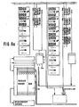
- Each input group contains - as already shown 4 and 5 is explained - an hour and a minute counter each (cf., for example, 106, 108 for the ON- 127 and the OFF-switching time group 146 ).
- Each input branch has its own acknowledgment group, e.g. 113 for the hour digit ON or e.g. 117 the minute position ON or the days of the week 142 ON (see explanation of Fig. 4 and 5). Programs with fixed weekdays are naturally not acknowledged because they have not been entered.
- the channel selector group 307 has corresponding acknowledgment groups.
- the partial memories for example, are just as systematic as the modules described so far. 318 of the intermediate register 319 constructed from matching memory elements, for example. an ON switching time register 168, an OFF switching time register 169, a weekday ON 143, a weekday OFF register 147, a weekday ON 145, a weekday OFF address register, and a channel selection Register.
- Each acknowledgment causes the content of the next entry point to be shown on the display, which is effected by the relevant acknowledgment group 553 via the line concerned, so that the input is then operated.
- This operator guidance takes place both by flashing the colon after the function selection as well as after each completed entry of the ON switching time, first the hours, then the minutes, then by blinking the symbols for the days of the week, also after completing or acknowledging the choice of days of the week, etc., whose symbols remain. Pressing the setting buttons without prior confirmation after entering the days of the week causes the OFF switching time display to flash, Entering and acknowledging the hours and minutes - individually by themselves - causes the channel display to flash, their acknowledgment or places cause the acknowledged channel display to stop or to be replaced.
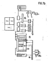
- an additional circuit is set up in the time control group (FIG. 8), with which the time-of-day switching program brought forward and entered for a selected day, in particular Sunday, is also temporally related for other days so that it can be processed, e.g. for Thursday, Friday, Saturday and Sunday are processed in the same way.
- the relevant additional circuit consists of a preselection counter 564, which is operated by means of the manual switch button 565 - actuated n times - for n days before Sunday to run this program.
- the preset counter is reset after each day of the program memory 556 by the weekday signal 566 of the clock 559 until the end of the reset to zero - when "F 0" appears on the display - for example. in the line for the OFF switching times - the sequence of the switching program is normal again.
- both the circuit arrangement of the new time program switching device has an extreme structure and is modular in every detail, and consequently the program parts are accordingly constructed from identical stages and components.
- this is also expressed by the fact that a single actuating key 102, a single acknowledgment key 104 and a single function selection key 183 are sufficient for the operation for the selection of all partial programs, so that each of the function groups can be selected almost in time, namely the input groups, the acknowledgment groups, the ON - and OFF-time switch block to activate the day of the week selection, the aforementioned three single connecting lines 101, 103, 184 being sufficient.
Landscapes
- Physics & Mathematics (AREA)
- General Physics & Mathematics (AREA)
- Electric Clocks (AREA)
- Oscillators With Electromechanical Resonators (AREA)
- Communication Control (AREA)
- Programmable Controllers (AREA)
Priority Applications (1)
| Application Number | Priority Date | Filing Date | Title |
|---|---|---|---|
| AT89114429T ATE88287T1 (de) | 1988-08-11 | 1989-08-04 | Elektronische digitale schalt- und/oder regelvorrichtung, insbesondere schaltuhr. |
Applications Claiming Priority (2)
| Application Number | Priority Date | Filing Date | Title |
|---|---|---|---|
| DE3827327A DE3827327A1 (de) | 1988-08-11 | 1988-08-11 | Bedieneinrichtung und -anordnung fuer ein elektronisches digitales schalt- und/oder regelgeraet, insbesondere schaltuhr |
| DE3827327 | 1988-08-11 |
Publications (3)
| Publication Number | Publication Date |
|---|---|
| EP0354487A2 true EP0354487A2 (fr) | 1990-02-14 |
| EP0354487A3 EP0354487A3 (fr) | 1991-07-17 |
| EP0354487B1 EP0354487B1 (fr) | 1993-04-14 |
Family
ID=6360669
Family Applications (1)
| Application Number | Title | Priority Date | Filing Date |
|---|---|---|---|
| EP89114429A Expired - Lifetime EP0354487B1 (fr) | 1988-08-11 | 1989-08-04 | Appareil électronique, numérique, de commutation et/ou de régulation, en particulier interrupteur horaire |
Country Status (4)
| Country | Link |
|---|---|
| EP (1) | EP0354487B1 (fr) |
| AT (1) | ATE88287T1 (fr) |
| DE (2) | DE3827327A1 (fr) |
| ES (1) | ES2040422T3 (fr) |
Cited By (2)
| Publication number | Priority date | Publication date | Assignee | Title |
|---|---|---|---|---|
| WO1994016400A1 (fr) * | 1993-01-05 | 1994-07-21 | Honeywell Inc. | Interface d'utilisateur a usages multiples |
| EP0825501A1 (fr) * | 1996-08-16 | 1998-02-25 | LEGRAND GmbH | Dispositif de commutation contrÔlé par programme avec commande à menu |
Family Cites Families (2)
| Publication number | Priority date | Publication date | Assignee | Title |
|---|---|---|---|---|
| DE3123711A1 (de) * | 1981-06-15 | 1983-01-05 | Dieter Gräßlin Feinwerktechnik, 7742 St Georgen | "digitalelektronisches zeitschaltwerk" |
| DE3668508D1 (de) * | 1985-04-03 | 1990-03-01 | Siemens Ag | Bedienungseinheit fuer eine schaltuhr. |
-
1988
- 1988-08-11 DE DE3827327A patent/DE3827327A1/de not_active Withdrawn
-
1989
- 1989-08-04 AT AT89114429T patent/ATE88287T1/de active
- 1989-08-04 DE DE8989114429T patent/DE58904056D1/de not_active Expired - Fee Related
- 1989-08-04 EP EP89114429A patent/EP0354487B1/fr not_active Expired - Lifetime
- 1989-08-04 ES ES198989114429T patent/ES2040422T3/es not_active Expired - Lifetime
Cited By (2)
| Publication number | Priority date | Publication date | Assignee | Title |
|---|---|---|---|---|
| WO1994016400A1 (fr) * | 1993-01-05 | 1994-07-21 | Honeywell Inc. | Interface d'utilisateur a usages multiples |
| EP0825501A1 (fr) * | 1996-08-16 | 1998-02-25 | LEGRAND GmbH | Dispositif de commutation contrÔlé par programme avec commande à menu |
Also Published As
| Publication number | Publication date |
|---|---|
| ES2040422T3 (es) | 1993-10-16 |
| EP0354487B1 (fr) | 1993-04-14 |
| DE58904056D1 (de) | 1993-05-19 |
| DE3827327A1 (de) | 1990-02-15 |
| EP0354487A3 (fr) | 1991-07-17 |
| ATE88287T1 (de) | 1993-04-15 |
Similar Documents
| Publication | Publication Date | Title |
|---|---|---|
| DE3030246C2 (de) | Dateneingabevorrichtung | |
| DE883968C (de) | Durch Impulse gesteuerte elektronische Anordnung, insbesondere Rechengeraet | |
| EP0069046B1 (fr) | Appareil électronique de régulation | |
| DE2259957B2 (de) | Elektronische Uhr | |
| DE2700165A1 (de) | Uhr in integrierter schaltungstechnik | |
| DE3026128C2 (fr) | ||
| DE2922925C2 (de) | Als Haupt- oder Nebenuhr einsetzbare programmierte Digitaluhr | |
| DE3039843C2 (fr) | ||
| EP0092211B1 (fr) | Dispositif de commutation de programme de temps électronique | |
| DE69517641T2 (de) | Programmierbare elektronische Vorrichtung zur Steuerung von Bewässerungssystemen | |
| EP0167848B1 (fr) | Dispositif et procédé pour la programmation et l'affichage des moments de commutation d'un interrupteur horaire numérique | |
| EP0354487B1 (fr) | Appareil électronique, numérique, de commutation et/ou de régulation, en particulier interrupteur horaire | |
| DE2813477C3 (de) | Elektronische Kalenderanzeigevorrichtung | |
| DE2320104C3 (de) | Mehrzweckbefehlsgeber | |
| DE2649197C2 (de) | Elektronische Uhr | |
| EP0197336B1 (fr) | Dispositif de commande pour interrupteur horaire | |
| DE69024695T2 (de) | Elektronische Anzeigevorrichtung zum Anzeigen der Kalenderinformation | |
| DE4210874C2 (de) | Elektronische Zeitschaltuhr | |
| DE2857653C2 (fr) | ||
| DE2716387C3 (de) | Elektronische Uhr | |
| DE69006807T2 (de) | Weltuhr. | |
| DE2826836C2 (de) | Verfahren und Vorrichtung zum Abrufen und Ablegen von Daten oder Programmen | |
| DE4335990C2 (de) | Vorrichtung zur Programmierung | |
| DE9312338U1 (de) | Elektrische Schaltvorrichtung mit einer Schaltuhr | |
| AT384512B (de) | Schaltung fuer einen programmierbaren fernsehempfaenger |
Legal Events
| Date | Code | Title | Description |
|---|---|---|---|
| PUAI | Public reference made under article 153(3) epc to a published international application that has entered the european phase |
Free format text: ORIGINAL CODE: 0009012 |
|
| AK | Designated contracting states |
Kind code of ref document: A2 Designated state(s): AT BE CH DE ES FR GB IT LI NL SE |
|
| 17P | Request for examination filed |
Effective date: 19900322 |
|
| RAP1 | Party data changed (applicant data changed or rights of an application transferred) |
Owner name: LEGRAND GMBH |
|
| PUAL | Search report despatched |
Free format text: ORIGINAL CODE: 0009013 |
|
| AK | Designated contracting states |
Kind code of ref document: A3 Designated state(s): AT BE CH DE ES FR GB IT LI NL SE |
|
| 17Q | First examination report despatched |
Effective date: 19920206 |
|
| GRAA | (expected) grant |
Free format text: ORIGINAL CODE: 0009210 |
|
| AK | Designated contracting states |
Kind code of ref document: B1 Designated state(s): AT BE CH DE ES FR GB IT LI NL SE |
|
| PG25 | Lapsed in a contracting state [announced via postgrant information from national office to epo] |
Ref country code: SE Effective date: 19930414 Ref country code: NL Effective date: 19930414 Ref country code: BE Effective date: 19930414 |
|
| REF | Corresponds to: |
Ref document number: 88287 Country of ref document: AT Date of ref document: 19930415 Kind code of ref document: T |
|
| REF | Corresponds to: |
Ref document number: 58904056 Country of ref document: DE Date of ref document: 19930519 |
|
| ET | Fr: translation filed | ||
| ITF | It: translation for a ep patent filed | ||
| GBT | Gb: translation of ep patent filed (gb section 77(6)(a)/1977) |
Effective date: 19930616 |
|
| PG25 | Lapsed in a contracting state [announced via postgrant information from national office to epo] |
Ref country code: AT Effective date: 19930804 |
|
| PG25 | Lapsed in a contracting state [announced via postgrant information from national office to epo] |
Ref country code: LI Effective date: 19930831 Ref country code: CH Effective date: 19930831 |
|
| NLV1 | Nl: lapsed or annulled due to failure to fulfill the requirements of art. 29p and 29m of the patents act | ||
| REG | Reference to a national code |
Ref country code: ES Ref legal event code: FG2A Ref document number: 2040422 Country of ref document: ES Kind code of ref document: T3 |
|
| PLBE | No opposition filed within time limit |
Free format text: ORIGINAL CODE: 0009261 |
|
| STAA | Information on the status of an ep patent application or granted ep patent |
Free format text: STATUS: NO OPPOSITION FILED WITHIN TIME LIMIT |
|
| 26N | No opposition filed | ||
| REG | Reference to a national code |
Ref country code: CH Ref legal event code: PL |
|
| PGFP | Annual fee paid to national office [announced via postgrant information from national office to epo] |
Ref country code: GB Payment date: 19980803 Year of fee payment: 10 |
|
| PGFP | Annual fee paid to national office [announced via postgrant information from national office to epo] |
Ref country code: FR Payment date: 19980806 Year of fee payment: 10 Ref country code: ES Payment date: 19980806 Year of fee payment: 10 |
|
| PGFP | Annual fee paid to national office [announced via postgrant information from national office to epo] |
Ref country code: DE Payment date: 19980924 Year of fee payment: 10 |
|
| PG25 | Lapsed in a contracting state [announced via postgrant information from national office to epo] |
Ref country code: GB Free format text: LAPSE BECAUSE OF NON-PAYMENT OF DUE FEES Effective date: 19990804 |
|
| PG25 | Lapsed in a contracting state [announced via postgrant information from national office to epo] |
Ref country code: ES Free format text: LAPSE BECAUSE OF NON-PAYMENT OF DUE FEES Effective date: 19990805 |
|
| GBPC | Gb: european patent ceased through non-payment of renewal fee |
Effective date: 19990804 |
|
| PG25 | Lapsed in a contracting state [announced via postgrant information from national office to epo] |
Ref country code: FR Free format text: LAPSE BECAUSE OF NON-PAYMENT OF DUE FEES Effective date: 20000428 |
|
| PG25 | Lapsed in a contracting state [announced via postgrant information from national office to epo] |
Ref country code: DE Free format text: LAPSE BECAUSE OF NON-PAYMENT OF DUE FEES Effective date: 20000601 |
|
| REG | Reference to a national code |
Ref country code: FR Ref legal event code: ST |
|
| REG | Reference to a national code |
Ref country code: ES Ref legal event code: FD2A Effective date: 20000911 |
|
| PG25 | Lapsed in a contracting state [announced via postgrant information from national office to epo] |
Ref country code: IT Free format text: LAPSE BECAUSE OF NON-PAYMENT OF DUE FEES;WARNING: LAPSES OF ITALIAN PATENTS WITH EFFECTIVE DATE BEFORE 2007 MAY HAVE OCCURRED AT ANY TIME BEFORE 2007. THE CORRECT EFFECTIVE DATE MAY BE DIFFERENT FROM THE ONE RECORDED. Effective date: 20050804 |