EP0355555B1 - Schaltung zur Verarbeitung eines sich zeitlich ändernden Signals - Google Patents
Schaltung zur Verarbeitung eines sich zeitlich ändernden Signals Download PDFInfo
- Publication number
- EP0355555B1 EP0355555B1 EP89114568A EP89114568A EP0355555B1 EP 0355555 B1 EP0355555 B1 EP 0355555B1 EP 89114568 A EP89114568 A EP 89114568A EP 89114568 A EP89114568 A EP 89114568A EP 0355555 B1 EP0355555 B1 EP 0355555B1
- Authority
- EP
- European Patent Office
- Prior art keywords
- time
- circuit
- coupled
- path
- varying signal
- Prior art date
- Legal status (The legal status is an assumption and is not a legal conclusion. Google has not performed a legal analysis and makes no representation as to the accuracy of the status listed.)
- Expired - Lifetime
Links
- 239000003990 capacitor Substances 0.000 claims description 36
- 230000001934 delay Effects 0.000 claims description 5
- 230000000153 supplemental effect Effects 0.000 claims 2
- 230000003111 delayed effect Effects 0.000 description 3
- 238000005070 sampling Methods 0.000 description 3
- 238000010586 diagram Methods 0.000 description 2
- 230000001902 propagating effect Effects 0.000 description 2
- 230000005540 biological transmission Effects 0.000 description 1
- 230000008878 coupling Effects 0.000 description 1
- 238000010168 coupling process Methods 0.000 description 1
- 238000005859 coupling reaction Methods 0.000 description 1
- 230000005669 field effect Effects 0.000 description 1
- 230000000644 propagated effect Effects 0.000 description 1
Images

Classifications
-
- G—PHYSICS
- G11—INFORMATION STORAGE
- G11C—STATIC STORES
- G11C27/00—Electric analogue stores, e.g. for storing instantaneous values
- G11C27/02—Sample-and-hold arrangements
- G11C27/024—Sample-and-hold arrangements using a capacitive memory element
- G11C27/026—Sample-and-hold arrangements using a capacitive memory element associated with an amplifier
Definitions
- This invention relates generally to circuits for processing a time-varying signal.
- the present invention relates generally to high speed circuits where the timing of signals occurring in a main path and an auxiliary path, such as in a feedback path, is critical.
- a sample-and-hold circuit one circuit type where this is particularly true is a sample-and-hold circuit.
- Sample-and-hold circuits are often used on the input of an analog-to-digital converter for providing a stable input signal for the converter.
- High speed converters are becoming very common as digital signal processing of high frequency signals is undertaken.
- Sample-and-hold circuits typically employ an analog switching device, generally referred to as a sampling gate, for periodically connecting a capacitor to an input signal to be sampled.
- a sampling gate for periodically connecting a capacitor to an input signal to be sampled.
- the capacitor is connected to the signal so that it charges and discharges to track the voltage level of the signal.
- the switch is turned off, disconnecting the capacitor from the input signal.
- the capacitor holds that voltage level existing on the input signal at the time the capacitor is disconnected.
- the charge on the capacitor should stay constant, providing a constant output voltage.
- the capacitor is also typically connected to a high impedance input of a buffer amplifier which provides the hold output signal of the sample-and-hold circuit, the high impedance input ensuring minimal discharge of the capacitor during the hold phase of the circuit operation.
- the switches used in sample and hold circuits are typically either Schottky diode bridges or field-effect transistors.
- the diode bridge which is perhaps the simplest of the switches, is switched by a pair of controlled current sources.
- Circuit 10 includes an input terminal 12 for receiving the input signal to be sampled. This terminal is connected to an input buffer amplifier 14.
- the output of amplifier 14 is input into a switch in the form of a Schottky diode bridge 18 which is controlled by a pair of current sources 20 and 22. These current sources receive a control signal from a control signal generator 23.
- the diode bridge adjacent each current source has blow-by current shunt diodes 24 and 26 which are biased by fixed voltage sources 28 and 30.
- the output of the switch is coupled to a hold capacitor 32, one side of which is grounded. This capacitor tracks the input signal during the track state and holds a charge proportional to the input signal when in the hold state.
- the capacitor 32 is coupled to an output amplifier 34 for outputting the output signal on an output terminal 36.
- the bias voltages for diodes 24 and 26 are bootstrapped from the circuit output through a bias circuit 38.
- This circuit configuration is more effective than prior versions of the circuit. However, in high speed applications, it tends to have limited use because of the longer settling time required by the bootstrapping arrangement. This is due primarily to the time delay in the signal propagating to the output and then feeding back to the operative circuit component, such as the switch or amplifier.
- sample-and-hold circuits also typically have a hold capacitor which is grounded so that it must take the complete charge of the input signal. Thus, changes in charge take more time than if less stored charge was required.
- the invention is characterized by the features of claim 1.
- the present invention overcomes the disadvantage of prior art circuits generally, and sample-and-hold circuits in particular, such as the one shown in Fig. 1, by providing a referencing voltage source on a main signal path which has fast settling times.
- This aspect of the invention is provided in a circuit for processing a time-varying signal comprising a main subcircuit coupled between an input and an output terminal for conducting the time-varying signal along a first path.
- An auxiliary subcircuit substantially identical to at least a portion of the main subcircuit and coupled between the input terminal and the main subcircuit conducts the time-varying signal along a second path.
- a delay subcircuit delays the time of propagation of the time-varying signal along one of the first and second paths so that the time-varying signal at a selected point along the first path has a predetermined time relationship with respect to the time-varying signal traveling along the second path at the point it is fed to the main subcircuit.
- a sample-and-hold circuit for sampling a time-varying signal. Included are a main sample-and-hold subcircuit and an auxiliary sample-and-hold subcircuit.
- Each sample-and-hold subcircuit comprises an input buffer amplifier coupled to an input terminal, a diode-bridge switch responsive to a control signal and coupled to the input buffer amplifier, a charge-holding capacitor coupled to the switch, and an output buffer amplifier coupled to the capacitor.
- the output of the auxiliary output amplifier further is coupled to the main switch and the output of the main output amplifier is coupled to the output terminal.
- a control-signal generator generates the signal for controlling the switches such that the same part of the time-varying signal passing through the main and auxiliary subcircuits is sampled.
- a delay subcircuit delays the time-varying signal passing through the main subcircuit such that the time-varying signals traveling through the main and auxiliary subcircuits reach the main switch at substantially the same time.
- One aspect of the present invention also further enhances high speed operation by providing a hold capacitor which only tracks and holds a small charge, thereby charging more quickly.
- this is provided by an auxiliary sample-and-hold subcircuit wherein an auxiliary charge-holding capacitor is coupled to a switch for holding substantially the voltage of the time-varying signal received through the auxiliary switch.
- a main charge-holding capacitor coupled between the outputs of main and auxiliary switches holds the difference in voltage between the voltage of the time-varying signal received through the main switch and the voltage on the auxiliary capacitor.
- Fig. 1 is a block diagram of a conventional sample-and-hold circuit.
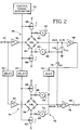
- Fig. 2 is a block diagram of a sample-and-hold circuit made according to the present invention.
- Figs. 3 and 4 are sample waveforms of a signal in the circuit of Fig. 2 at two different times.
- Fig. 1 is described in the section entitled Background of the Invention.
- a sample-and-hold circuit 40 made according to the invention is shown in Fig. 2.
- the circuit of Fig. 2 similar to the circuit of Fig. 1, includes an input terminal 42, a main sample-and-hold subcircuit 44, and an output terminal 46, all defining what may be referred to as a first signal path.
- a second signal path is defined by an auxiliary sample-and-hold subcircuit 48 substantially identical in its main elements, as will be seen, as main subcircuit 44.
- a delay element 50 such as is provided conventionally by a transmission line, is posed between the input terminal 42 and the input to main subcircuit 44.
- Main subcircuit 44 includes an input buffer amplifier 52 of conventional and well known design connected to delay unit 50.
- the output of the amplifier 52 is also input into a conventional Schottky diode bridge forming a sampling gate switch 56, similar to bridge 18 of Fig. 1. It is driven by two controllable current sources 58 and 60.
- Sources 58 and 60 are controlled by a control signal received from a control signal generator 62 of conventional design.
- the generator 62 generates the signals which determine when the circuit is in a track state and when it is in a hold state. When current is flowing through the switch 56, it is in a track state, and correspondingly, when current is not flowing through the switch 56, it is in a hold state.
- the control signal passes through another delay element 64 for delaying the time that the signal reaches the current sources 58, 60 of the main subcircuit 44.
- the diode bridge also has a pair of blow-by current shunting diodes 66 and 68 and associated voltage sources 70 and 72. These are fed from a bias subcircuit 74.
- the output of the switch 56 is connected to one terminal of a hold or memory capacitor 76 which is connected between the main and auxiliary subcircuits as will be further described below.
- the switch output is also input to an output buffer amplifier 78 of conventional design, the output of which is connected to output terminal 46.
- Auxiliary subcircuit 48 is structured substantially identically to main subcircuit 44 and includes an input amplifier 82, diode bridge switch 84, current sources 86 and 88, blow-by diodes 90 and 92, associated voltage sources 94 and 96, and output amplifier 98.
- the output of amplifier 98 is used as the voltage source for bias circuit 74.
- the current sources 86; 88 are connected to receive the control signals directly from generator 62.
- a hold capacitor 100 is connected conventionally between the output of switch 84 and ground. Capacitor 76 is connected between the two outputs of switches 56 and 84.
- Auxiliary subcircuit 48 is thus a basic sample-and-hold circuit without bootstrapping of the blow-by diodes associated with the switch 84.
- circuit 40 is a pair of substantially identical sample-and-hold circuits, essentially in parallel, and both receiving the same input signal. However, one of the circuits receives the input signal delayed relative to the other. The circuit which receives the input signal is used to generate what would normally be the feedback or bootstrap voltages for the circuit with the delayed signal.
- Figs. 3 and 4 The preferred timing of the two signals in the two circuits is illustrated in Figs. 3 and 4.
- an input signal 102 is shown as it appears in the two subcircuits at two points in time.
- the propagation delay of the signal through the subcircuit components is in equal increments, as represented by the vertical dashed lines.
- Fig. 3 represents the existence of the signal at a first time, T1.
- the signal level is lowest at 104, the input to auxiliary input amplifier 82 and rises through the auxiliary subcircuit to its highest point 106 at the output of bias circuit 74.
- this time varying input signal does not in actuality have the same voltage level as it progresses through the circuit. However, it is shown as having values of the same scale throughout so that its progress through the circuit will be more apparent.
- the figures are thus primarily illustrative of the timing of the signal.
- the delay provided by delay element 50 is set to be equal to the time of propagation of the signal through the input amplifier 82, switch 84 and output amplifier 98 of the auxiliary subcircuit 48. If the various delays are not equal, then the difference in propagation time through the bias circuit 74 and the main input amplifier 52 would also need to be included. Thus, the signal at point 108 is at the input of the main input amplifier 52, while the output signal, assuming the circuit is in the track state, is shown by point 110. At instant T1 control signal generator 62 outputs a signal to switch to the hold state. Thus, auxiliary switch 84 switches so that the signal at the output of the switch at point 112 is held on capacitor 100.
- Fig. 4 illustrates the location of the input signal throughout circuit 40 at a second instant in time, T2.
- 112 of the signal is at the output of main switch 56.
- the input signal voltage has been held on capacitor 100 since T1, as represented by the horizontal line segment 114.
- the held value of the signal has thus had time to propagate along path two through auxiliary output amplifier 98, bias circuit 74 and switch 56.
- the signal has propagated through delay element 50, main amplifier 52 and switch 56.
- the control signal from generator 62 has also been delayed by element 64 so that the change from track state to hold state in the main subcircuit occurs at time T2.
- the signals along paths one and two thus arrive at switch 56 in phase. That is to say, the same point on the input signal reaches the switch 56 along the two paths at substantially the same time. Since the auxiliary subcircuit 48 has been in a hold state since time T1, the voltage levels have had time to settle and the biasing signal fed to the main subcircuit 44 is advanced over what it would be if the output of the main subcircuit 44 was bootstrapped. There is thus a savings in the delay time that it would take the signal to propagate through the main output amplifier 78, bias subcircuit 74 and switch 56 so that it could settle to a relatively steady state output.
- FIG. 2 An important aspect of the present invention is illustrated in the circuit of Fig. 2 wherein the hold capacitor 76 of the main sample-and-hold subcircuit 44 is coupled between the output of the main switch 56 and the auxiliary capacitor 100. Since the auxiliary capacitor 100 is coupled to ground, it holds the voltage of the input signal on it. The main capacitor 76 therefore only holds any voltage differential which exists between the voltage on the auxiliary capacitor 100 and the voltage output from the main switch 56. Thus, the main capacitor 76 has very small charge variations with variations in the input signal. The main diode bridge bias current is therefore much lower than that of the auxiliary diode bridge 84. Further, the main input buffer 52 has less driving to do.
- delay times have been treated idealistically and simplistically, it will be appreciated by those skilled in the art that the actual delay times incorporated in practicing the present invention are preferably verified, if not actually determined, on an empirical basis, for each circuit, so that inherent variations in circuit components can be compensated for.
Landscapes
- Electronic Switches (AREA)
- Amplifiers (AREA)
- Logic Circuits (AREA)
Claims (6)
- Schaltung zur Verarbeitung eines sich zeitlich ändernden Signals mit
einer in einen ersten Weg (50, 52, 56) zwischen einem Eingangsanschluß (42) und einem Ausgangsanschluß (46) gekoppelten Hauptschaltung (44) zur Führung des sich zeitlich ändernden Signals längs des ersten Weges vom Eingangsanschluß (42) durch die Hauptschaltung (44) zum Ausgangsanschluß (46); und
einer an einen Rückkoppelpunkt der Hauptschaltung (44) gekoppelten Hilfsschaltung (48),
dadurch gekennzeichnet, daß
die Hilfsschaltung (48) im wesentlichen identisch mit der Hauptschaltung (44) und zur Führung des sich zeitlich ändernden Signals längs eines zweiten Weges (82, 84, 74, 98) vom Eingangsanschluß (42) zur Hauptschaltung (44) am Rückkoppelpunkt zwischen den Einganschluß (42) und den Rückkoppelpunkt der Hauptschaltung (44) gekoppelt ist, und
Mittel (50, 62, 64) zur Verzögerung der Ausbreitungszeit des sich zeitlich ändernden Signals längs des ersten Weges (50, 52, 56) zum Rückkoppelpunkt vorgesehen sind, so daß das sich zeitlich ändernde Signal an einem ausgewählten Punkt längs des ersten Weges (50, 52, 56) einen vorgegebenen Zeitzusammenhang mit dem sich zeitlich ändernden Signal längs des zweiten Weges (82, 84, 74, 98) am Rückkoppelpunkt hat, wodurch das sich zeitlich ändernde Signal längs des ersten Weges (50, 52, 56) den Rückkoppelpunkt im wesentlichen im gleichen Zeitpunkt wie das sich zeitlich ändernde Signal längs des zweiten Weges (82, 84, 74, 98) erreicht. - Schaltung nach Anspruch 1, in der die Hauptschaltung (44) und die Hilfsschaltung (48) durch
zum Empfang des sich zeitlich ändernden Signals gekoppelte Schaltermittel (56, 84);
Mittel (58, 60, 86, 88) zur Steuerung der Schaltermittel (56, 84) in Abhängigkeit eines Steuersignals; und
einen zum Empfang des sich zeitlich ändernden Signals von den Schaltermitteln (56, 84) gekoppelten Kondensator (76, 100), wobei der Kondensator (100) für die Hilfsschaltung (48) mit dem einen Ende an die Schaltermittel (84) und den zweiten Weg (98, 74) und mit dem anderen Ende an ein Referenzpotential und der Kondensator (76) für die Hauptschaltung (44) zwischen das eine Ende des Hilfsschaltungskondensators (100) und den Ausgangsanschluß (46) gekoppelt ist,
gekennzeichnet sind. - Schaltung nach Anspruch 2, in der die Verzögerungsmittel durch
erste Verzögerungsmittel (50), die zum Empfang des sich zeitlich ändernden Signals für die Hauptschaltung (44) als Teil des ersten Weges (50, 52, 56) an den Eingangsanschluß (42) gekoppelt sind;
Steuersignal-Generatormittel (62), die zur Lieferung des Steuersignals für die Hauptschaltermittel (56) und die Hilfsschaltermittel (84) gekoppelt sind; und
zweite, zwischen die Steuersignal-Generatormittel (62) und die Hauptschaltermittel (56) gekoppelte Verzögerungsmittel (64), wobei die Verzögerungen der ersten Verzögerungsmittel (50) und der zweiten Verzögerungsmittel (64) im Sinne der Realisierung des vorgegebenen Zeitzusammenhangs eingestellt sind,
gekennzeichnet sind. - Schaltung nach Anspruch 1, in der der erste Weg (50, 52, 56) durch
zum Empfang des sich zeitlich ändernden Signals an den Eingangsanschluß (42) gekoppelte Verzögerungsmittel (50); einen zum Empfang des sich zeitlich ändernden Signals von den Verzögerungsmitteln (50) gekoppelten Eingangspufferverstärker (52) ; und
zur Übertragung des sich zeitlich ändernden Signals vom Eingangspufferverstärker (52) zum Ausgangsanschluß (46) in Abhängigkeit von einem Steuersignal zwischen den Eingangspufferverstärker (52) und den Ausgangsanschluß (46) gekoppelte Schaltermittel (56)
gekennzeichnet ist. - Schaltung nach den Ansprüchen 1 bis 4, in der der zweite Weg (74, 98) durch
eine zwischen die Hilfsschaltung (48) und die Hauptschaltung (44) gekoppelte Zusatzschaltung (74) zur Verarbeitung des sich zeitlich ändernden Signals längs des zweiten Weges (74, 98), wobei die Verzögerungsmittel (50, 62, 64) Ausbreitungsverzögerung des die Zusatzschaltung (74) durchlaufenden Signals kompensieren, gekennzeichnet ist. - Schaltung nach den Ansprüchen 1 bis 5, in der der vorgegebene Zeitzusammenhang durch im wesentlichen keine Zeitverzögerung zwischen den sich zeitlich ändernden Signalen vom ersten Weg (50, 52, 56) und zweiten Weg (74, 98) gekennzeichnet ist.
Applications Claiming Priority (2)
| Application Number | Priority Date | Filing Date | Title |
|---|---|---|---|
| US229195 | 1988-08-08 | ||
| US07/229,195 US4885545A (en) | 1988-08-08 | 1988-08-08 | High speed circuit with supporting auxiliary circuit |
Publications (2)
| Publication Number | Publication Date |
|---|---|
| EP0355555A1 EP0355555A1 (de) | 1990-02-28 |
| EP0355555B1 true EP0355555B1 (de) | 1994-12-21 |
Family
ID=22860190
Family Applications (1)
| Application Number | Title | Priority Date | Filing Date |
|---|---|---|---|
| EP89114568A Expired - Lifetime EP0355555B1 (de) | 1988-08-08 | 1989-08-07 | Schaltung zur Verarbeitung eines sich zeitlich ändernden Signals |
Country Status (4)
| Country | Link |
|---|---|
| US (1) | US4885545A (de) |
| EP (1) | EP0355555B1 (de) |
| JP (1) | JPH0279299A (de) |
| DE (1) | DE68920089T2 (de) |
Families Citing this family (12)
| Publication number | Priority date | Publication date | Assignee | Title |
|---|---|---|---|---|
| DE69026740D1 (de) * | 1989-02-28 | 1996-06-05 | Fujitsu Ltd | Fehler absorbierendes System in einem neuronalen Rechner |
| US5239181A (en) * | 1990-12-31 | 1993-08-24 | The United States Of America As Represented By The Secretary Of The Navy | Bridge type optoelectronic sample and hold circuit |
| US5124576A (en) * | 1991-03-26 | 1992-06-23 | Unitrode Corporation | Track and hold amplifier |
| US5631553A (en) * | 1993-05-31 | 1997-05-20 | Universite Du Quebec A Trois-Rivieres | High precision RF vector analysis system based on synchronous sampling |
| US5552784A (en) * | 1994-06-30 | 1996-09-03 | Northrop Grumman Corporation | Distortion reduction circuit for analog to digital converter system |
| US5745003A (en) * | 1996-09-11 | 1998-04-28 | Schlumberger Technologies Inc. | Driver circuits for IC tester |
| US6118330A (en) * | 1999-02-19 | 2000-09-12 | Bossard; Peter R. | Looped circuit and associated method for controlling the relationship between current and capacitance in CMOS and BICMOS circuit design |
| US6323696B1 (en) * | 1999-12-07 | 2001-11-27 | Hughes Electronics Corporation | Sample and hold circuit |
| DE10207676A1 (de) * | 2002-02-22 | 2003-09-04 | Philips Intellectual Property | Schaltungsanordnung für einen stromgesteuerten Widerstand mit erweitertem Linearitätsbereich |
| DE10207675A1 (de) * | 2002-02-22 | 2003-09-04 | Philips Intellectual Property | Schaltungsanordnung für einen stromgesteuerten Widerstand mit erweitertem Linearitätsbereich |
| GB0416803D0 (en) * | 2004-07-27 | 2004-09-01 | Wood John | Rotary flash ADC |
| JP4872574B2 (ja) * | 2006-09-28 | 2012-02-08 | 澁谷工業株式会社 | 容器処理装置 |
Family Cites Families (11)
| Publication number | Priority date | Publication date | Assignee | Title |
|---|---|---|---|---|
| US3789304A (en) * | 1972-10-19 | 1974-01-29 | Bell Telephone Labor Inc | Gated dividing circuit with reduced time variation between gating and an output signal |
| US3942124A (en) * | 1973-12-26 | 1976-03-02 | Tarczy Hornoch Zoltan | Pulse synchronizing apparatus and method |
| DE3224442A1 (de) * | 1982-06-30 | 1984-01-05 | Siemens AG, 1000 Berlin und 8000 München | Anordnung zur erzeugung von quasizufallsfolgen im ami-code |
| CA1207036A (en) * | 1982-09-29 | 1986-07-02 | Hans P. Lie | Switched capacitor feedback sample-and-hold circuit |
| US4518921A (en) * | 1982-10-18 | 1985-05-21 | At&T Bell Laboratories | Track and hold circuit |
| US4542304A (en) * | 1982-12-20 | 1985-09-17 | At&T Bell Laboratories | Switched capacitor feedback sample-and-hold circuit |
| US4584559A (en) * | 1984-06-13 | 1986-04-22 | Tektronix, Inc. | Dual rank sample and hold circuit and method |
| US4659945A (en) * | 1985-04-01 | 1987-04-21 | Tektronix, Inc. | Sampling bridge |
| JPS6381698A (ja) * | 1986-09-25 | 1988-04-12 | Hiroshi Nakamura | サンプリングホ−ルド回路 |
| FR2604819B1 (fr) * | 1986-10-03 | 1988-12-09 | Thomson Semiconducteurs | Echantillonneur-bloqueur a haute frequence d'echantillonnage |
| JPS6396800A (ja) * | 1986-10-13 | 1988-04-27 | Sony Corp | Cmosサンプルホ−ルド回路 |
-
1988
- 1988-08-08 US US07/229,195 patent/US4885545A/en not_active Expired - Fee Related
-
1989
- 1989-07-29 JP JP1197898A patent/JPH0279299A/ja active Pending
- 1989-08-07 EP EP89114568A patent/EP0355555B1/de not_active Expired - Lifetime
- 1989-08-07 DE DE68920089T patent/DE68920089T2/de not_active Expired - Fee Related
Also Published As
| Publication number | Publication date |
|---|---|
| DE68920089D1 (de) | 1995-02-02 |
| US4885545A (en) | 1989-12-05 |
| JPH0279299A (ja) | 1990-03-19 |
| DE68920089T2 (de) | 1995-05-04 |
| EP0355555A1 (de) | 1990-02-28 |
Similar Documents
| Publication | Publication Date | Title |
|---|---|---|
| EP0540052B1 (de) | Brummspannungsfreier Phasendetektor unter Verwendung von zwei Abtast-Halteschaltungen | |
| EP0355555B1 (de) | Schaltung zur Verarbeitung eines sich zeitlich ändernden Signals | |
| KR0170410B1 (ko) | 마스터슬레이브형 플립플롭회로 | |
| EP0851434B1 (de) | Abtast- und Halteschaltung und Halbleiteranordnung damit | |
| US5373294A (en) | Current switch for a high speed DAC | |
| US4862016A (en) | High speed, low drift sample and hold circuit | |
| US4686489A (en) | Triggered voltage controlled oscillator using fast recovery gate | |
| US5302863A (en) | CMOS peak amplitude detector | |
| US5148054A (en) | High accuracy MOSFET-switched sampling circuit | |
| US7023254B2 (en) | Duty ratio corrector, and memory device having the same | |
| EP0139499A2 (de) | Abtast-Halte-Schaltungen | |
| US6249154B1 (en) | Process of controlling a switch of a switched-capacitance device, and corresponding switched-capacitance device | |
| US4893036A (en) | Differential signal delay circuit | |
| EP0345156A2 (de) | Analogschalter | |
| US6094155A (en) | Dual reference voltage buffer and method for updating CDAC bit capacitors | |
| US6794919B1 (en) | Devices and methods for automatically producing a clock signal that follows the master clock signal | |
| US6437620B1 (en) | Circuit and method for multi-phase alignment | |
| JPS60501085A (ja) | 演算増幅器の改良されたスル−レ−トを達成するための回路 | |
| US7136000B1 (en) | Selective offset adjustment of a track and hold circuit | |
| JPH0362050B2 (de) | ||
| EP0101947B1 (de) | Treiberschaltung | |
| US5180930A (en) | Method and apparatus for reducing the effects of feedback switch charge injection into a plurality of serially connected sample data comparators | |
| US6552622B1 (en) | Oscillator having reduced sensitivity to supply voltage changes | |
| JPH057800B2 (de) | ||
| US5874842A (en) | Sample and hold circuit having quick resetting function |
Legal Events
| Date | Code | Title | Description |
|---|---|---|---|
| PUAI | Public reference made under article 153(3) epc to a published international application that has entered the european phase |
Free format text: ORIGINAL CODE: 0009012 |
|
| AK | Designated contracting states |
Kind code of ref document: A1 Designated state(s): DE FR GB NL |
|
| 17P | Request for examination filed |
Effective date: 19900608 |
|
| RAP1 | Party data changed (applicant data changed or rights of an application transferred) |
Owner name: TEKTRONIX, INC. |
|
| RAP1 | Party data changed (applicant data changed or rights of an application transferred) |
Owner name: TEKTRONIX, INC. |
|
| 17Q | First examination report despatched |
Effective date: 19930202 |
|
| GRAA | (expected) grant |
Free format text: ORIGINAL CODE: 0009210 |
|
| AK | Designated contracting states |
Kind code of ref document: B1 Designated state(s): DE FR GB NL |
|
| PG25 | Lapsed in a contracting state [announced via postgrant information from national office to epo] |
Ref country code: NL Effective date: 19941221 Ref country code: FR Effective date: 19941221 |
|
| REF | Corresponds to: |
Ref document number: 68920089 Country of ref document: DE Date of ref document: 19950202 |
|
| NLV1 | Nl: lapsed or annulled due to failure to fulfill the requirements of art. 29p and 29m of the patents act | ||
| EN | Fr: translation not filed | ||
| PG25 | Lapsed in a contracting state [announced via postgrant information from national office to epo] |
Ref country code: GB Effective date: 19950807 |
|
| PLBE | No opposition filed within time limit |
Free format text: ORIGINAL CODE: 0009261 |
|
| STAA | Information on the status of an ep patent application or granted ep patent |
Free format text: STATUS: NO OPPOSITION FILED WITHIN TIME LIMIT |
|
| 26N | No opposition filed | ||
| GBPC | Gb: european patent ceased through non-payment of renewal fee |
Effective date: 19950807 |
|
| PG25 | Lapsed in a contracting state [announced via postgrant information from national office to epo] |
Ref country code: DE Effective date: 19960501 |