EP0355670A2 - Amplificateur de fréquences micro-ondes à bruit bas, à gain, stabilité et commande de bruit optimaux - Google Patents
Amplificateur de fréquences micro-ondes à bruit bas, à gain, stabilité et commande de bruit optimaux Download PDFInfo
- Publication number
- EP0355670A2 EP0355670A2 EP89115048A EP89115048A EP0355670A2 EP 0355670 A2 EP0355670 A2 EP 0355670A2 EP 89115048 A EP89115048 A EP 89115048A EP 89115048 A EP89115048 A EP 89115048A EP 0355670 A2 EP0355670 A2 EP 0355670A2
- Authority
- EP
- European Patent Office
- Prior art keywords
- terminal
- resistor
- amplifier
- amplifier according
- filter means
- Prior art date
- Legal status (The legal status is an assumption and is not a legal conclusion. Google has not performed a legal analysis and makes no representation as to the accuracy of the status listed.)
- Granted
Links
- JBRZTFJDHDCESZ-UHFFFAOYSA-N AsGa Chemical compound [As]#[Ga] JBRZTFJDHDCESZ-UHFFFAOYSA-N 0.000 claims abstract description 16
- 229910001218 Gallium arsenide Inorganic materials 0.000 claims abstract description 15
- 230000005540 biological transmission Effects 0.000 claims abstract description 14
- 238000001914 filtration Methods 0.000 claims abstract description 14
- 239000003990 capacitor Substances 0.000 claims description 16
- 230000005669 field effect Effects 0.000 claims description 7
- 239000004020 conductor Substances 0.000 description 15
- 238000005457 optimization Methods 0.000 description 8
- 239000010409 thin film Substances 0.000 description 6
- PNEYBMLMFCGWSK-UHFFFAOYSA-N aluminium oxide Inorganic materials [O-2].[O-2].[O-2].[Al+3].[Al+3] PNEYBMLMFCGWSK-UHFFFAOYSA-N 0.000 description 4
- 230000000903 blocking effect Effects 0.000 description 4
- 238000010586 diagram Methods 0.000 description 3
- PCHJSUWPFVWCPO-UHFFFAOYSA-N gold Chemical compound [Au] PCHJSUWPFVWCPO-UHFFFAOYSA-N 0.000 description 3
- 239000010931 gold Substances 0.000 description 3
- 229910052737 gold Inorganic materials 0.000 description 3
- 230000006641 stabilisation Effects 0.000 description 3
- 238000011105 stabilization Methods 0.000 description 3
- 230000000087 stabilizing effect Effects 0.000 description 2
- 239000000758 substrate Substances 0.000 description 2
- 238000013459 approach Methods 0.000 description 1
- 238000005094 computer simulation Methods 0.000 description 1
- 239000002184 metal Substances 0.000 description 1
- 229910052751 metal Inorganic materials 0.000 description 1
- 239000004065 semiconductor Substances 0.000 description 1
- 230000001131 transforming effect Effects 0.000 description 1
Images

Classifications
-
- H—ELECTRICITY
- H03—ELECTRONIC CIRCUITRY
- H03F—AMPLIFIERS
- H03F1/00—Details of amplifiers with only discharge tubes, only semiconductor devices or only unspecified devices as amplifying elements
- H03F1/34—Negative-feedback-circuit arrangements with or without positive feedback
- H03F1/342—Negative-feedback-circuit arrangements with or without positive feedback in field-effect transistor amplifiers
-
- H—ELECTRICITY
- H03—ELECTRONIC CIRCUITRY
- H03F—AMPLIFIERS
- H03F1/00—Details of amplifiers with only discharge tubes, only semiconductor devices or only unspecified devices as amplifying elements
- H03F1/26—Modifications of amplifiers to reduce influence of noise generated by amplifying elements
-
- H—ELECTRICITY
- H03—ELECTRONIC CIRCUITRY
- H03F—AMPLIFIERS
- H03F3/00—Amplifiers with only discharge tubes or only semiconductor devices as amplifying elements
- H03F3/189—High-frequency amplifiers, e.g. radio frequency amplifiers
- H03F3/19—High-frequency amplifiers, e.g. radio frequency amplifiers with semiconductor devices only
- H03F3/193—High-frequency amplifiers, e.g. radio frequency amplifiers with semiconductor devices only with field-effect devices
- H03F3/1935—High-frequency amplifiers, e.g. radio frequency amplifiers with semiconductor devices only with field-effect devices with junction-FET devices
-
- H—ELECTRICITY
- H03—ELECTRONIC CIRCUITRY
- H03F—AMPLIFIERS
- H03F2200/00—Indexing scheme relating to amplifiers
- H03F2200/144—Indexing scheme relating to amplifiers the feedback circuit of the amplifier stage comprising a passive resistor and passive capacitor
-
- H—ELECTRICITY
- H03—ELECTRONIC CIRCUITRY
- H03F—AMPLIFIERS
- H03F2200/00—Indexing scheme relating to amplifiers
- H03F2200/372—Noise reduction and elimination in amplifier
Definitions
- the subject invention relates to electronic amplifiers, and more particularly, to a low noise gallium arsenide (GaAs) field effect transistor microwave amplifier.
- GaAs gallium arsenide
- GaAs metal semiconductor field effect transistors provide the lowest noise figure and are the best devices for low noise microwave amplifier applications. In such applications, a noise figure of 2.0 dB or less may be specified for particular frequencies.
- a drawback of present GaAs MESFET devices is that they are extremely reflective, i.e., have a very high reflection coefficient, and hence are very unstable, i.e., readily oscillate. In the design of a low noise amplifier, it is desirable to stabilize the GaAs MESFET, while retaining its intrinsic low noise characteristic.
- the prior art approaches have employed both resistive parallel feedback and resistive-capacitive parallel feedback stabilizing networks in GaAs amplifier circuits.
- the resistive-capacitive parallel feedback preserves the low noise characteristic of the device, but results in poor stability.
- Resistive-parallel feedback provides some stability, but the noise figure is an order of magnitude higher than resistive-capacitive parallel feedback.
- a parallel feedback network for a GaAs field effect transistor amplifier including a resistor-capacitor-resistor (R-C-R) series arrangement.
- R-C-R resistor-capacitor-resistor
- the use of separate resistors itself in the R-C-R series arrangement contributes to improved circuit performance.
- the R-C-R series circuit is used in conjunction with a filtering means for attenuating noise generated by the resistors.
- the filtering means is implemented by disposing the R-C-R series arrangement between a set of filtering circuits, which are disposed at opposite ends of the feedback loop.
- the invention provides the ability to simultaneously and optimally control stability, gain and noise, parameters which frequently interact and have proven difficult to control in low noise microwave amplifier design.
- the amplifier stability factor can be kept higher than 1 over a multioctave frequency range without destroying the intrinsic low noise characteristic or gain of the GaAs device. It is possible, for example, to achieve a stability factor of higher than 1 over a range of frequencies from 1 to 18 gigahertz (GHz) using an R-C-R arrangement with a filter means as hereafter disclosed.
- GHz gigahertz
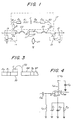
- FIG. 1 illustrates a low noise amplifier employing a GaAs MESFET 11 and R-C-R parallel feedback in accordance with the preferred embodiment of the invention.
- the amplifier includes input and output RF matching circuits 13, 15, the GaAs MESFET 11, and the parallel feedback loop 17.
- the MESFET 11 has terminals comprising a gate G, a drain D and a source S, the source S being shown connected to RF ground through bond wires 27.
- the MESFET 11 may be an NE 71000 as manufactured by NEC Corporation.
- the input RF matching circuit 13 includes a transmission line (TRL) element Z6 and a TRL element Z5.
- the TRL element Z6 is connected at one terminal through bond wires 23 to the gate G of the MESFET 11.
- a second terminal of the TRL element Z6 provides the input 19 to the amplifier and is also connected to a first terminal of the TRL element Z5, the other terminal of which is connected to DC ground.
- the output RF matching circuit 15 includes a TRL element Z7 connected by bonding wires 25 to the drain D of the MESFET 11.
- the second terminal of the TRL element Z7 provides the output 21 of the amplifier.
- the TRL element Z8 is connected at a first terminal to the output terminal 21 and is connected to RF ground at its second terminal.
- the RF matching circuits 13, 15 are standard matching circuits with their values chosen to match the input and output impedances of the MESFET 11, respectively. While the circuits 13, 15 shown are “L” type matching circuits, other configurations could be used, such as "T” or " ⁇ ” matching circuits.
- the parallel feedback loop 17 includes two filtering networks 18, 20, each of which includes a pair of transmission line elements.
- the first filtering network 18 comprises TRL elements Z1 and Z2, while the second filtering network 20 comprises third and fourth TRL elements Z3, Z4.
- the parallel feedback network 17 includes the first filtering network 18 in series with an R-C-R series circuit, in turn connected in series with the second filtering network 20.
- the resistor-capacitor-resistor (R1-C-R2) circuitry in between the filters 18, 20 provides amplifier stabilization and gain adjustment.
- the two resistors R1, R2 arranged in the R-C-R configuration aid each other in keeping the amplifier stability factor K from falling below 1 across a multioctave frequency range as wide as 1 to 18 GHz.
- Computer simulations show that removing either one of the two resistors R1, R2 from the circuit of FIG. 1 will immediately lower the stability factor K.
- the resistors R1, R2 generate thermal noise which, if uncompensated, would detract from noise performance. Accordingly, the filtering networks 18, 20 are used to attenuate the noise generated in the feedback loop 17 to minimize the noise added into the device noise figure of the transistor 11.
- the filters 18, 20 themselves are standard microwave quarter-wave transmission line section filters. Two transmission line sections in each filter 18, 20 have been found to provide sufficient noise rejection in the preferred embodiment.
- Computer optimization of the circuit of FIG. 1 may be employed to optimize the amplifier for desired stability, gain and noise figure simultaneously.
- Optimization may be achieved by selecting initial component values for each element Z1, Z2, Z3, Z4, R1, R2, C of the feedback loop 17, placing limits on the variation in values of those elements, and causing a computer to vary the values within the limits set to select an optimum combination.
- the Touchstone (TM) software available from EESOF, Westlake Village, California may be used for this purpose, such use being within the skill of those of ordinary skill in the art. Defining the limits of a resistance value and a capacitance value for gain adjustment and stabilization of a GaAs microwave amplifier is also within the skill of those ordinarily skilled in the art. According to the invention, it has been found that splitting the resistance value into two physically discrete resistors R1, R2 in R-C-R fashion contributes to improved stability.
- the TRL elements Z1, Z2, Z3 and Z4 are initially selected as one-quarter wavelength transmission line sections, the wavelength being determined, as known in the art, by a selected center frequency of operation. It is found through optimization that better performance is achieved in the design described in connection with FIG. 2 when the TRL elements Z1, Z2, Z3 and Z4 are slightly unequal to one-quarter wavelength. Accordingly, in the embodiment of FIG. 2, the impedance of the TRL element Z1 is selected by optimization to be higher than the TRL element Z2, and at the same time the transmission line elements Z1 and Z2, after optimization, are each chosen to be unequal to one-quarter wavelength. Similarly, in the second filtering network 20 of FIG.
- the TRL element Z4 is selected by optimization to be a lower impedance than the TRL element Z3, and the TRL elements Z3, Z4 after optimization are selected to be unequal to one-quarter wavelength.
- optimization may dictate different relationships between the length and the impedance values of the TRL element pairs Z1, Z2 and Z3, Z4.
- FIG. 2 illustrates a thin film microwave distributed integrated circuit layout of a GaAs MESFET amplifier constructed according to the preferred embodiment to provide a noise figure of 2.0 or less in the S-band frequency range.
- such circuits typically are fabricated of gold or another suitable conductor deposited on an alumina substrate.
- the resistor R1 has the value of 1,000 ohms
- the capacitor C has the value of 33 picofarads
- the resistor R2 has the value of 300 ohms. Removal of either resistor R1 or R2 from the circuit will result in the stability factor falling below 1 at some frequencies in the 1 to 18-GHz range.
- the transmission line elements Z1-Z8 are preferably fabricated of gold deposited on .025-inch (.0635 cm) thick alumina. By appropriately transforming the impedances into microstrip lines, the lengths and widths of the filter TRL elements Z1, Z2, Z3 and Z4 and the remaining TRL elements Z5-Z8 may be determined.
- the following table shows the respective length and width of each of the transmission line elements Z1-Z8 for a microstrip circuit (FIG.
- Additional elements of the circuit shown in FIG. 2 include the input DC blocking capacitor CB1 located in between conductors 41 and 43 and the output DC blocking capacitor CB2 located between conductors 59 and 61.
- Conductor pads 67, 68 and 70, each .050 x .050 inch (.127 x .127 cm) square, are used to connect the thin film resistor R1, the chip capacitor C and the thin film resistor R2 to the transmission line sections Z2 and Z3 of filters 18 and 20 in the feedback loop, completing the R-C-R portion of the feedback loop 17.
- FIG. 3 shows a microstrip cross-sectional view of the interconnection of the R-C-R stabilization network shown in FIG. 2.
- the thin film chip resistor R1 is connected between the TRL element Z2 and the conductor pad 70.
- a wire bond 72 is made to the chip capacitor C mounted on top of the conductor pad 70.
- the thin film chip resistor R2 is connected between the conductor pad 68 and the conductor pad 67.
- FIG. 2 further illustrates a number of grounding pads 45, 51, 53, 55 and conductor pads 47, 49, 57, 63, 65, which are provided to ground and interconnect various circuit elements.
- the TRL element Z5 which has an equivalent inductance denoted L1 is grounded by the ground pad 45.
- a chip capacitor C1 is connected to the source of the MESFET 11 and is grounded at one terminal by the ground pad 53.
- a chip capacitor C2 connected to the same source is mounted on the ground pad 51 and connected by a bond wire to the conductor pad 49.
- a thin film chip resistor R3 is connected between the two conductor pads 49, 47 and effectively grounded by a bond wire connection to the ground pad 51.
- the TRL element Z8 which has an equivalent inductance denoted L2, is connected at one terminal to conductor pad 59 and at the other terminal to the conductor pad 57.
- a chip capacitor C3 is connected from the conductor pad 57 to the ground pad 55. It may be noted that the grounding pads 45, 51, 53, 55 and conductor pads 47, 49, 57, 63, 65 are also preferably constructed of gold deposited on alumina, as known in the art.
- FIG. 4 illustrates the D.C. bias circuit for the MESFET 11.
- the gate G of the MESFET 11 is coupled to the input blocking capacitor CB1 and to ground through the inductance L1.
- the source S of the MESFET 11 is commonly connected to the capacitors C1, C2 and the resistor R3.
- the opposite terminals of these elements C1, C2, R3 are grounded.
- the drain D of the MESFET 11 is fed by a bias voltage source V d through the inductance L2 (which functions as a choke) and is serially connected to an output blocking capacitor CB2.
- the bypass capacitor C3 connects between the source voltage V D and ground. Design of a biasing circuit such as that of FIG. 4 is well within the skill of those of ordinary skill in the art.
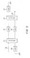
- FIG. 5 Since the amplifier described above has low noise but only a moderate voltage standing wave ratio (VSWR) ( ⁇ 2.0:1), a circuit such as shown in FIG. 5 may be employed in a system where both a low VSWR and a good noise figure are required.
- two amplifiers 78, 80 each constructed like that of FIG. 1 or FIG. 2, are connected in a microwave circuit with hybrid couplers 81, 83.
- the circuit of FIG. 5 is a conventional hybrid circuit.
- the hybrid couplers 81, 83 preferably comprise 3-dB Lange couplers, as well known in the art.
- the input to the circuit of FIG. 5 is at a first terminal 88 of the input coupler 81.
- the second terminal of the input coupler 81 is grounded through a 50-ohm load 85, as known in the art.
- the output coupler 83 has one terminal grounded through a 50-ohm load 87 and a second terminal forming the output terminal 89 of the circuit.
- the first and second amplifiers 78, 80 according to the preferred embodiment are connected between the terminals of the two couplers 81, 83, again as known in the art. In such an application, it is possible to achieve a VSWR much better than 1.25:1, while retaining a low noise figure of below 2 dB, along with required stability and gain, even though losses of the hybrids are directly added to the noise figure in this arrangement.
Landscapes
- Engineering & Computer Science (AREA)
- Power Engineering (AREA)
- Microwave Amplifiers (AREA)
- Amplifiers (AREA)
Applications Claiming Priority (2)
| Application Number | Priority Date | Filing Date | Title |
|---|---|---|---|
| US07/232,728 US4878033A (en) | 1988-08-16 | 1988-08-16 | Low noise microwave amplifier having optimal stability, gain, and noise control |
| US232728 | 1999-01-19 |
Publications (3)
| Publication Number | Publication Date |
|---|---|
| EP0355670A2 true EP0355670A2 (fr) | 1990-02-28 |
| EP0355670A3 EP0355670A3 (en) | 1990-10-17 |
| EP0355670B1 EP0355670B1 (fr) | 1994-07-27 |
Family
ID=22874307
Family Applications (1)
| Application Number | Title | Priority Date | Filing Date |
|---|---|---|---|
| EP89115048A Expired - Lifetime EP0355670B1 (fr) | 1988-08-16 | 1989-08-16 | Amplificateur de fréquences micro-ondes à bruit bas, à gain, stabilité et commande de bruit optimaux |
Country Status (6)
| Country | Link |
|---|---|
| US (1) | US4878033A (fr) |
| EP (1) | EP0355670B1 (fr) |
| JP (1) | JPH02113610A (fr) |
| CA (1) | CA1284360C (fr) |
| DE (1) | DE68917050T2 (fr) |
| IL (1) | IL91376A0 (fr) |
Cited By (3)
| Publication number | Priority date | Publication date | Assignee | Title |
|---|---|---|---|---|
| GB2268348A (en) * | 1992-06-30 | 1994-01-05 | Texas Instruments Ltd | Noise trap for a high frequency transistor amplifier |
| GB2272121A (en) * | 1992-10-26 | 1994-05-04 | Plessey Semiconductors Ltd | Low noise r.f. amplifiers using capacitative feedback. |
| ES2065221A1 (es) * | 1992-04-23 | 1995-02-01 | Univ Madrid Complutense | Procedimiento para diseñar un amplificador de microondas con especificaciones determinadas de perdidas por reflexiones, figura de ruido y ganancia de transduccion. |
Families Citing this family (4)
| Publication number | Priority date | Publication date | Assignee | Title |
|---|---|---|---|---|
| FR2633119B1 (fr) * | 1988-06-21 | 1990-11-09 | Labo Electronique Physique | Circuit actif hyperfrequences du type passe-tout |
| JPH0785528B2 (ja) * | 1989-12-25 | 1995-09-13 | 日本電気株式会社 | 高出力マイクロ波ミリ波トランジスタ安定化回路 |
| DE19507133C2 (de) * | 1995-03-01 | 1998-06-04 | Siemens Ag | Schaltungsanordnung eines Ultra-Breitband Empfängers |
| GB2411062B (en) | 2004-02-11 | 2007-11-28 | Nujira Ltd | Resonance suppression for power amplifier output network |
Family Cites Families (3)
| Publication number | Priority date | Publication date | Assignee | Title |
|---|---|---|---|---|
| US32132A (en) * | 1861-04-23 | Steam-trap | ||
| JPS6012683B2 (ja) | 1977-03-11 | 1985-04-03 | 株式会社日立製作所 | 映像信号再生回路 |
| JPH109003A (ja) * | 1996-06-27 | 1998-01-13 | Hitachi Constr Mach Co Ltd | エンジンの停止装置 |
-
1988
- 1988-08-16 US US07/232,728 patent/US4878033A/en not_active Expired - Fee Related
-
1989
- 1989-08-16 DE DE68917050T patent/DE68917050T2/de not_active Expired - Fee Related
- 1989-08-16 CA CA000608519A patent/CA1284360C/fr not_active Expired - Fee Related
- 1989-08-16 JP JP1211216A patent/JPH02113610A/ja active Granted
- 1989-08-16 EP EP89115048A patent/EP0355670B1/fr not_active Expired - Lifetime
- 1989-08-22 IL IL91376A patent/IL91376A0/xx unknown
Non-Patent Citations (5)
| Title |
|---|
| 1983 IEEE MTT-S INTERNATIONAL MICROWAVE SYMPOSIUM DIGEST, Boston, MA, 31st May - 3rd June 1983, pages 44-45, IEEE, New York, US; P.N. RIGBY et al.: "Broadband monolithic low-noise feedback amplifiers" * |
| CONFERENCE PROCEEDINGS OF THE 14TH EUROPEAN MICROWAVE CONFERENCE, Liège, 10th-13th September 1984, pages 488-493; C.E. WEITZEL et al.: "Monolithic GaAs wideband low noise RLC feedback amplifiers" * |
| ELECTRONIC ENGINEERING, vol. 59, no. 726, June 1987, page 78, Woolwich, London, GB; "MMIC's adopted for microwave amplifiers" * |
| MICROWAVE JOURNAL, vol. 28, no. 10, October 1985, pages 155,156,158,160,162,164,166,168, Dedham, MA, US; A.A. SWEET: "A parametric study of the behavior of 1 micron GaAs FET amplifiers" * |
| THE TRANSACTIONS OF THE IECE OF JAPAN, SECT. E, vol. E-68, no. 2, February 1985, pages 98-101, Tokyo, JP; M. NISHIUMA et al.: "A GaAs monolithic low-noise negative feedback amplifier using a dual-gate MESFET" * |
Cited By (6)
| Publication number | Priority date | Publication date | Assignee | Title |
|---|---|---|---|---|
| ES2065221A1 (es) * | 1992-04-23 | 1995-02-01 | Univ Madrid Complutense | Procedimiento para diseñar un amplificador de microondas con especificaciones determinadas de perdidas por reflexiones, figura de ruido y ganancia de transduccion. |
| GB2268348A (en) * | 1992-06-30 | 1994-01-05 | Texas Instruments Ltd | Noise trap for a high frequency transistor amplifier |
| GB2268348B (en) * | 1992-06-30 | 1996-01-03 | Texas Instruments Ltd | Noise reduction circuit |
| GB2272121A (en) * | 1992-10-26 | 1994-05-04 | Plessey Semiconductors Ltd | Low noise r.f. amplifiers using capacitative feedback. |
| US5378997A (en) * | 1992-10-26 | 1995-01-03 | Plessey Semiconductors Limited | Low noise amplifier with capacitive feedback |
| GB2272121B (en) * | 1992-10-26 | 1996-03-27 | Plessey Semiconductors Ltd | Amplifiers |
Also Published As
| Publication number | Publication date |
|---|---|
| JPH0586081B2 (fr) | 1993-12-09 |
| JPH02113610A (ja) | 1990-04-25 |
| IL91376A0 (en) | 1990-04-29 |
| EP0355670A3 (en) | 1990-10-17 |
| DE68917050T2 (de) | 1994-11-10 |
| EP0355670B1 (fr) | 1994-07-27 |
| US4878033A (en) | 1989-10-31 |
| CA1284360C (fr) | 1991-05-21 |
| DE68917050D1 (de) | 1994-09-01 |
Similar Documents
| Publication | Publication Date | Title |
|---|---|---|
| US4788511A (en) | Distributed power amplifier | |
| US6400240B2 (en) | Integrated resonance circuit consisting of a parallel connection of a microstrip line and a capacitor | |
| EP0949754B1 (fr) | Circuit et module d'amplificateur de puissance à haute fréquence | |
| CN100459121C (zh) | 具内部偏馈射频功率晶体管 | |
| US6346859B1 (en) | Microwave amplifier with reduced beat noise | |
| EP0401632B1 (fr) | Méthode et appareil d'adaptation d'impédance à large bande | |
| US5233313A (en) | High power field effect transistor amplifier | |
| US4841253A (en) | Multiple spiral inductors for DC biasing of an amplifier | |
| US4864250A (en) | Distributed amplifier having improved D.C. biasing and voltage standing wave ratio performance | |
| US6946934B2 (en) | Transmission line and semiconductor integrated circuit device | |
| EP0600548A1 (fr) | Circuit amplificateur à micro-onde à forme de construction compacte utilisable en cascade | |
| US6239670B1 (en) | Short-stub matching circuit | |
| US4947136A (en) | Variable gain distributed amplifier | |
| EP0355670B1 (fr) | Amplificateur de fréquences micro-ondes à bruit bas, à gain, stabilité et commande de bruit optimaux | |
| KR100529581B1 (ko) | 초고주파 윌켄슨 전력분배기 | |
| US6127894A (en) | High frequency shunt feedback amplifier topology | |
| US4912430A (en) | Current source as a microwave biasing element | |
| JP3303845B2 (ja) | 内部整合型出力fet | |
| US6320468B2 (en) | Method and system for suppressing oscillations in a multi-stage amplifier | |
| US7199667B2 (en) | Integrated power amplifier arrangement | |
| US4118672A (en) | Attenuation equalizer having constant resistance | |
| JPH04287507A (ja) | 電界効果トランジスタ増幅器 | |
| JP3051430B2 (ja) | マイクロ波集積回路 | |
| JPS62271502A (ja) | マイクロ波装置の整合回路 | |
| Takenaka et al. | An MMIC active LC filter |
Legal Events
| Date | Code | Title | Description |
|---|---|---|---|
| PUAI | Public reference made under article 153(3) epc to a published international application that has entered the european phase |
Free format text: ORIGINAL CODE: 0009012 |
|
| 17P | Request for examination filed |
Effective date: 19890907 |
|
| AK | Designated contracting states |
Kind code of ref document: A2 Designated state(s): DE FR GB IT |
|
| PUAL | Search report despatched |
Free format text: ORIGINAL CODE: 0009013 |
|
| AK | Designated contracting states |
Kind code of ref document: A3 Designated state(s): DE FR GB IT |
|
| 17Q | First examination report despatched |
Effective date: 19930906 |
|
| GRAA | (expected) grant |
Free format text: ORIGINAL CODE: 0009210 |
|
| AK | Designated contracting states |
Kind code of ref document: B1 Designated state(s): DE FR GB IT |
|
| PG25 | Lapsed in a contracting state [announced via postgrant information from national office to epo] |
Ref country code: IT Free format text: LAPSE BECAUSE OF FAILURE TO SUBMIT A TRANSLATION OF THE DESCRIPTION OR TO PAY THE FEE WITHIN THE PRE;WARNING: LAPSES OF ITALIAN PATENTS WITH EFFECTIVE DATE BEFORE 2007 MAY HAVE OCCURRED AT ANY TIME BEFORE 2007. THE CORRECT EFFECTIVE DATE MAY BE DIFFERENT FROM THE ONE RECORDED.SCRIBED TIME-LIMIT Effective date: 19940727 |
|
| ET | Fr: translation filed | ||
| REF | Corresponds to: |
Ref document number: 68917050 Country of ref document: DE Date of ref document: 19940901 |
|
| PLBE | No opposition filed within time limit |
Free format text: ORIGINAL CODE: 0009261 |
|
| STAA | Information on the status of an ep patent application or granted ep patent |
Free format text: STATUS: NO OPPOSITION FILED WITHIN TIME LIMIT |
|
| PGFP | Annual fee paid to national office [announced via postgrant information from national office to epo] |
Ref country code: FR Payment date: 19950710 Year of fee payment: 7 |
|
| PGFP | Annual fee paid to national office [announced via postgrant information from national office to epo] |
Ref country code: GB Payment date: 19950718 Year of fee payment: 7 |
|
| 26N | No opposition filed | ||
| PGFP | Annual fee paid to national office [announced via postgrant information from national office to epo] |
Ref country code: DE Payment date: 19950721 Year of fee payment: 7 |
|
| PG25 | Lapsed in a contracting state [announced via postgrant information from national office to epo] |
Ref country code: GB Effective date: 19960816 |
|
| GBPC | Gb: european patent ceased through non-payment of renewal fee |
Effective date: 19960816 |
|
| PG25 | Lapsed in a contracting state [announced via postgrant information from national office to epo] |
Ref country code: FR Effective date: 19970430 |
|
| PG25 | Lapsed in a contracting state [announced via postgrant information from national office to epo] |
Ref country code: DE Effective date: 19970501 |
|
| REG | Reference to a national code |
Ref country code: FR Ref legal event code: ST |