EP0355965A2 - Procédé pour obtenir une commande et un empêchement sélectif d'adhésion en conducteurs à film épais - Google Patents
Procédé pour obtenir une commande et un empêchement sélectif d'adhésion en conducteurs à film épais Download PDFInfo
- Publication number
- EP0355965A2 EP0355965A2 EP89306821A EP89306821A EP0355965A2 EP 0355965 A2 EP0355965 A2 EP 0355965A2 EP 89306821 A EP89306821 A EP 89306821A EP 89306821 A EP89306821 A EP 89306821A EP 0355965 A2 EP0355965 A2 EP 0355965A2
- Authority
- EP
- European Patent Office
- Prior art keywords
- circuit board
- printed circuit
- board assembly
- controllably
- adherent
- Prior art date
- Legal status (The legal status is an assumption and is not a legal conclusion. Google has not performed a legal analysis and makes no representation as to the accuracy of the status listed.)
- Granted
Links
Images


Classifications
-
- H—ELECTRICITY
- H05—ELECTRIC TECHNIQUES NOT OTHERWISE PROVIDED FOR
- H05K—PRINTED CIRCUITS; CASINGS OR CONSTRUCTIONAL DETAILS OF ELECTRIC APPARATUS; MANUFACTURE OF ASSEMBLAGES OF ELECTRICAL COMPONENTS
- H05K3/00—Apparatus or processes for manufacturing printed circuits
- H05K3/40—Forming printed elements for providing electric connections to or between printed circuits
- H05K3/4092—Integral conductive tabs, i.e. conductive parts partly detached from the substrate
-
- H—ELECTRICITY
- H10—SEMICONDUCTOR DEVICES; ELECTRIC SOLID-STATE DEVICES NOT OTHERWISE PROVIDED FOR
- H10W—GENERIC PACKAGES, INTERCONNECTIONS, CONNECTORS OR OTHER CONSTRUCTIONAL DETAILS OF DEVICES COVERED BY CLASS H10
- H10W70/00—Package substrates; Interposers; Redistribution layers [RDL]
- H10W70/01—Manufacture or treatment
- H10W70/05—Manufacture or treatment of insulating or insulated package substrates, or of interposers, or of redistribution layers
- H10W70/098—Applying pastes or inks, e.g. screen printing
-
- H—ELECTRICITY
- H10—SEMICONDUCTOR DEVICES; ELECTRIC SOLID-STATE DEVICES NOT OTHERWISE PROVIDED FOR
- H10W—GENERIC PACKAGES, INTERCONNECTIONS, CONNECTORS OR OTHER CONSTRUCTIONAL DETAILS OF DEVICES COVERED BY CLASS H10
- H10W70/00—Package substrates; Interposers; Redistribution layers [RDL]
- H10W70/60—Insulating or insulated package substrates; Interposers; Redistribution layers
- H10W70/611—Insulating or insulated package substrates; Interposers; Redistribution layers for connecting multiple chips together
-
- H—ELECTRICITY
- H10—SEMICONDUCTOR DEVICES; ELECTRIC SOLID-STATE DEVICES NOT OTHERWISE PROVIDED FOR
- H10W—GENERIC PACKAGES, INTERCONNECTIONS, CONNECTORS OR OTHER CONSTRUCTIONAL DETAILS OF DEVICES COVERED BY CLASS H10
- H10W70/00—Package substrates; Interposers; Redistribution layers [RDL]
- H10W70/60—Insulating or insulated package substrates; Interposers; Redistribution layers
- H10W70/62—Insulating or insulated package substrates; Interposers; Redistribution layers characterised by their interconnections
- H10W70/65—Shapes or dispositions of interconnections
-
- H—ELECTRICITY
- H10—SEMICONDUCTOR DEVICES; ELECTRIC SOLID-STATE DEVICES NOT OTHERWISE PROVIDED FOR
- H10W—GENERIC PACKAGES, INTERCONNECTIONS, CONNECTORS OR OTHER CONSTRUCTIONAL DETAILS OF DEVICES COVERED BY CLASS H10
- H10W70/00—Package substrates; Interposers; Redistribution layers [RDL]
- H10W70/60—Insulating or insulated package substrates; Interposers; Redistribution layers
- H10W70/67—Insulating or insulated package substrates; Interposers; Redistribution layers characterised by their insulating layers or insulating parts
- H10W70/69—Insulating materials thereof
-
- H—ELECTRICITY
- H10—SEMICONDUCTOR DEVICES; ELECTRIC SOLID-STATE DEVICES NOT OTHERWISE PROVIDED FOR
- H10W—GENERIC PACKAGES, INTERCONNECTIONS, CONNECTORS OR OTHER CONSTRUCTIONAL DETAILS OF DEVICES COVERED BY CLASS H10
- H10W99/00—Subject matter not provided for in other groups of this subclass
-
- H—ELECTRICITY
- H05—ELECTRIC TECHNIQUES NOT OTHERWISE PROVIDED FOR
- H05K—PRINTED CIRCUITS; CASINGS OR CONSTRUCTIONAL DETAILS OF ELECTRIC APPARATUS; MANUFACTURE OF ASSEMBLAGES OF ELECTRICAL COMPONENTS
- H05K1/00—Printed circuits
- H05K1/02—Details
- H05K1/03—Use of materials for the substrate
- H05K1/0306—Inorganic insulating substrates, e.g. ceramic, glass
-
- H—ELECTRICITY
- H05—ELECTRIC TECHNIQUES NOT OTHERWISE PROVIDED FOR
- H05K—PRINTED CIRCUITS; CASINGS OR CONSTRUCTIONAL DETAILS OF ELECTRIC APPARATUS; MANUFACTURE OF ASSEMBLAGES OF ELECTRICAL COMPONENTS
- H05K1/00—Printed circuits
- H05K1/02—Details
- H05K1/09—Use of materials for the conductive, e.g. metallic pattern
- H05K1/092—Dispersed materials, e.g. conductive pastes or inks
-
- H—ELECTRICITY
- H10—SEMICONDUCTOR DEVICES; ELECTRIC SOLID-STATE DEVICES NOT OTHERWISE PROVIDED FOR
- H10W—GENERIC PACKAGES, INTERCONNECTIONS, CONNECTORS OR OTHER CONSTRUCTIONAL DETAILS OF DEVICES COVERED BY CLASS H10
- H10W72/00—Interconnections or connectors in packages
- H10W72/071—Connecting or disconnecting
- H10W72/072—Connecting or disconnecting of bump connectors
- H10W72/07251—Connecting or disconnecting of bump connectors characterised by changes in properties of the bump connectors during connecting
-
- H—ELECTRICITY
- H10—SEMICONDUCTOR DEVICES; ELECTRIC SOLID-STATE DEVICES NOT OTHERWISE PROVIDED FOR
- H10W—GENERIC PACKAGES, INTERCONNECTIONS, CONNECTORS OR OTHER CONSTRUCTIONAL DETAILS OF DEVICES COVERED BY CLASS H10
- H10W72/00—Interconnections or connectors in packages
- H10W72/20—Bump connectors, e.g. solder bumps or copper pillars; Dummy bumps; Thermal bumps
- H10W72/241—Dispositions, e.g. layouts
Definitions
- This invention relates to compositions of matter that are useful in forming conductive patterns on an insulating substrate or support member, techniques for forming such patterns, and assemblies using such a substrate.
- One such substrate is a circuit board having conductors which connect an electrical module to the circuit board to form a printed circuit board assembly.
- the term "electrical module” is intended to include any component, such as a semiconductor chip, a light emitting or detecting device, an emitting or detecting device of magnetic nature, a magnetic storage device, a capacitor, an inductor, a resistor, a crystal, a coil, a varactor, a thermistor, a resonator, transformers, and/or a connector that may be connected in an electrical circuit, an electro-optical circuit, an optical configuration, an electro-magnetic circuit and/or a magnetic configuration.
- a semiconductor chip such as a semiconductor chip, a light emitting or detecting device, an emitting or detecting device of magnetic nature, a magnetic storage device, a capacitor, an inductor, a resistor, a crystal, a coil, a varactor, a thermistor, a resonator, transformers, and/or a connector that may be connected in an electrical circuit, an electro-optical circuit, an optical configuration, an electro-magnetic circuit and/or
- a printed circuit board having a semiconductor chip or other electrical module attached thereto shall be denoted as a printed circuit board assembly. It will be convenient to generally discuss the invention with particular reference to a printed circuit board assembly including a semiconductor chip of the surface mount or flip-chip type.
- a printed circuit board assembly in accordance with the present invention is characterised by the features specified in the characterising portion of claim 1.
- controllably adherent conductor is used to describe a conductor which adheres to the circuit board during the manufacturing process, but which is free when being used to move (slide) along and/or lift off from the circuit board in response to stresses that may arise, for example, from thermal effects, to relieve such stresses.
- the printed circuit board also includes a pattern of firmly adherent conductors to which first ends of the controllably adherent conductors are connected. Second ends of the controllably adherent conductors are typically soldered to an electrical module, such as a silicon integrated circuit chip having metallic external contacts (bumps) extending from a surface thereof.
- an electrical module such as a silicon integrated circuit chip having metallic external contacts (bumps) extending from a surface thereof.
- controllably adherent conductor may itself also serve as an electrical module.
- One example of such is a film resistor.
- Controllably adherent conductors may be provided in various arrays and configurations, some of which are described below.
- the present invention also provides specific techniques useful for forming such controllably adherent conductors.
- a localized layer to be termed an inhibitor layer, intermediate between a circuit board and a portion of a conductive layer to achieve controlled adhesion for such portion of the conductive layer.
- Such controlled adhesion describes the property of a conductive layer overlying such inhibitor layer to lift off or slide along the printed circuit board in response to appropriate mechanical stress without fracture.
- it includes both the situation where the inhibitor layer remains bonded to the circuit board and separates from the overlying conductive layer and the situation where the inhibitor layer remains bonded to the conductive layer and together they separate from the circuit board.
- the localized use of an inhibitor layer allows one conductive layer to have one portion used as a firmly adherent conductor by placing it in direct contact with the circuit board and to have another portion used as a controllably adherent conductor by having it overlie an inhibitor layer.
- the inhibitor layer is formed preferably by printing and subsequently firing a composition comprising essentially a mixture of a finely divided refractory material (for example, alumina or aluminium nitride) and a glass frit, suspended in an organic vehicle.
- a finely divided refractory material for example, alumina or aluminium nitride
- a glass frit suspended in an organic vehicle.
- the glass frit is chosen to soften and wet both the surface of the circuit board and the refractory material at a temperature below the firing temperatures. This promotes bonding among the refractory particles and between the refractory particles and the surface of the circuit board.
- the refractory material chosen should have negligible chemical reaction with the conductor.
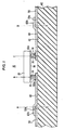
- the pcb assembly 10 comprises an electrical module 20 and a support member (circuit board, substrate) 40 having an insulative top surface 42 on which are printed firmly adherent conductors 50 and controllably adherent conductors 60.
- the electrical module 20 comprises an integrated circuit formed in a silicon chip of the flip chip or surface mount type, suitably covered by an insulating material (not shown) and having a plurality of external contacts 30 (for example, silver bumps) on a lower surface 34 thereof.
- the electrical module 20 may take various other forms as previously mentioned. It is to be noted that for illustrative purposes only, one electrical module 20 is shown. Typically, a printed circuit board assembly 10 contains a plurality of electrical modules 20 of different types.
- Support member 40 is of a suitable insulating material, such as alumina (Al2O3).
- the conductive pattern formed by the conductors 50 and 60 and the electrical module 20 form an electrical circuit of the printed circuit board assembly 10.
- the firmly adherent conductors 50 may be conventional. They are typically formed by depositing a patterned layer of a suitable ink or paste that, after firing, provides a firmly adherent conductive pattern that is compatible for use with a pattern of controllably adherent conductors 60.
- a firmly adherent conductor 50 may include copper, nickel, silver, palladium, platinum and gold and/or alloys thereof and/or other suitable metals and/or compounds to make it conductive.
- the electrical module 20 is secured to the firmly adherent conductors 50 by way of the controllably adherent conductors 60.
- Each external contact 30 of electrical module 20 is typically connected to one end 60a of a controllably adherent conductor 60 by means of a bond, such as a solder joint 32.
- the bond could be formed in various other ways, including use of a conductive adhesive epoxy or other conductive adhesive material, or the bond could be a weld.
- the other end 60b of the controllably adherent conductor 60 is bonded or fused in any suitable fashion to a contact portion 50a, typically formed by an end of a firmly adherent conductor 50.
- Firmly adherent conductors 50 are then deposited on the support member 40. This is done in conventional fashion and generally involves first screen printing a suitably patterned layer and then drying and firing the layer.
- the layer as printed is of an ink or paste that will form a firmly adhering conductive layer.
- the layer deposited is of a material commercially available from Dupont Electronics and known as Dupont 9161. It basically comprises conductive copper particles, adhesion promoters and a screening agent. Suitable other materials are available from other sources.
- the drying and firing is done in the manner prescribed by the supplier to sinter the copper particles together into a conductive layer which firmly adheres to the support member 40.
- controllably adherent conductors 60 are similarly formed by screen printing, drying and firing a layer of suitable composition.
- a second composition which is also found particularly useful, differs only in the composition of the binder, which now consists essentially of equal parts by weight of bismuth oxide and cuprous oxide, milled together.
- the cuprous oxide appears to serve primarily to promote adhesion.
- This frit can be also viewed as a mixture of bismuth oxide (0-70 percent) and the remainder a frit of the following composition by weight, 50-65 percent PbO, 5-15 percent PbF2, 20-30 percent SiO2, 0-5 percent Al2O3, and 5-15 percent B2O3 with a typical composition of this frit being by weight 55.4 percent PbO, 9.4 percent PbF2, 23.5 percent SiO2, 2.1 percent Al2O3 and 9.6 percent B2O3.
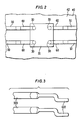
- FIG. 2 there is shown a top view of a portion of pcb assembly 10 which shows the controllably adherent conductors 60 as straight.
- Controllably adherent conductors 603 which have an S-shaped bend to reduce stress at the joint between a controllably adherent conductor 603 and a firmly adherent conductor 503.
- Conductors 503 and 603 are the same kind of conductors as conductors 50 and 60, of Figure 1 except for the bend in each controllably adherent conductor 603.
- Pcb assembly 105 is similar to pcb assembly 10 in Figure 1 and all corresponding parts thereof have the same reference number with a "5" added thereafter.
- Pcb assembly 105 is also similar to pcb assembly 104 of Figure 4 except that controllably adherent conductors 605 are S-shaped and are connected to firmly adherent conductors 505 which are connected to bonding (contact) pads 525. An electrical module to which controllably adherent conductors 605 are connected is not shown.
- Pcb assembly 107 is very similar to pcb assembly 10 of Figure 1 and to pcb assembly 104 of Figure 4 except the corresponding parts thereof have a "7" added to the last digit of the reference number.
- the rotation of the electrical module (chip) (not shown) to accommodate movement in the positions of its external contacts (not shown) and the solder joints (not shown).
- the length of the pairs of controllably adherent conductors 607 are chosen so that over a preselected operating temperature range, the changes in position of their first ends are such as to compensate for the changes in position of the external contacts (not shown).
- stresses on the solder joints are significantly limited and the reliability of pcb assembly 107 is significantly increased.
- a passage 92 (shown in dashed lines) can be formed through support member 409 and a conductor 94 can be passed therethrough to an opposite surface 96 of support member 409.
- a firmly adherent conductor 98 (shown in dashed lines) is attached to one end of conductor 94 which has a second end attached to bonding pad 529.
- support member 409 can be used as a double (two) sided printed circuit board.
- a central portion of support member 409, the portion shown as having centrally located contact 90, could have centrally located contact 90 deleted and could be instead adhesively attached to the top surface 429 by a heat conducting and electrically non-conducting epoxy or other material or compound (all not shown) to help conduct heat away from electrical module 209.
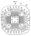
- Pcb assembly 1011 is essentially the same as pcb assembly 10 of Figure 1 except that it comprises a second electrical module 20a that is attached (soldered) via external contacts (for example, silver bumps) 30a by soldered joints 32a to portions 50b of firmly adherent conductors 50.
- Such attachment is typically used when electrical module 20a is sufficiently heavy such that if it were attached to controllably adherent conductors 60 it could endanger the integrity of the controllably adherent conductors 60 and cause them to crack and/or break.
- the electrical module 2014 has external contacts 31 thereof (which are attached to a lower surface 33 thereof) bonded, typically by solder joints 35 to (firmly adherent) portions 1014b of conductors 1014. Electrical module 2014 is typically attached to (firmly adherent) portions 1014b of conductors 1014 because in some cases it is sufficiently heavy such that if attached to portions 1014a it could endanger the integrity of portions 1014b of conductors 1014 and cause same to crack and/or break.
- the electrical module 2012 comprises an integrated circuit formed in a silicon chip of the flip chip or surface mount type, suitably covered by an insulating material (not shown) and having a plurality of external contacts 3012 (for example, silver bumps) on the lower surface 3412 thereof. These external contacts 3012 are connected to electrodes (not shown) of various circuit elements (not shown) of the electrical module 2012.
- the electrical module 2012 may take various other forms as previously mentioned. It is to be noted that for illustrative purposes only one electrical module 2012 is shown. Typically a printed circuit board assembly 1012 contains a plurality of electrical modules 2012 and 2014 of different types. It may, however, contain just one or more of electrical modules 2012.
- Each external contact 3012 of electrical module 2012 is typically connected to one part of a portion 1014a of a conductor 1014 by means of a bond, such as a solder joint 3212. All of the solder joints 3212 and 35 between both electrical modules 2012 and 2014 and the conductors 1014 could be formed in various other ways, including use of a conductive adhesive epoxy or other conductive adhesive material, or could be welds.
- the various materials involved are chosen such that mechanical stresses on the solder joints 3212 are significantly relieved by the ability of the solder joints 3212 to move relative to the support member 4012.
- the relative motion can be achieved in two basic fashions.
- the portions of the inhibitor layer 1016 under portions 1014a of conductors 1014 remain in place intimately bonded to the support member 4012 while the portions 1014a of the conductors 1014 are free to move along or lift off the inhibitor layer 1016.
- a third approach is to form the inhibitor layer by a composition that consists essentially of a finely divided refractory material (for example, alumina) suspended in an organic medium.
- a finely divided refractory material for example, alumina
- a fourth and presently preferred approach is to form the inhibitor layer by a composition that has a finely divided refractory material and a glass frit suspended in an organic medium.
- the glass frit is chosen to soften and wet both the surface of the circuit board and the refractory material, typically alumina, at a temperature below the firing temperatures. This promotes bonding among the refractory particles and between the refractory particles and the surface of the circuit board.
- the refractory material preferably an oxide such as alumina, should have negligible reaction with the conductive layer to be deposited over the inhibitor layer.
- compositions for use in printing the inhibitor layer 1016 included by weight: about 50 percent screening agent, 17 percent glass frit, and 33 percent alumina; and about 40 percent screening agent, about 20 percent glass frit and about 40 percent alumina.
- the screening agent used comprised by weight about 25 percent of a resin, typically Elvacite 2046, a product of E. I. Dupont de Nemours Inc. dissolved in a solvent, such as TEXANOL TM , a product that has been previously described, and the glass frit used comprised by weight between 60-75 percent PbO, 10-25 percent SiO2, 5-30 percent B2O3 and 0-10 percent Al2O3.
- a resin typically Elvacite 2046, a product of E. I. Dupont de Nemours Inc. dissolved in a solvent, such as TEXANOL TM , a product that has been previously described
- the glass frit used comprised by weight between 60-75 percent PbO, 10-25 percent SiO2, 5-30 percent B2O3 and 0-10 percent Al2O3.
- a solvent such as TEXANOL TM
- the glass frit used comprised by weight between 60-75 percent PbO, 10-25 percent SiO2, 5-30 percent B2O3
Landscapes
- Engineering & Computer Science (AREA)
- Microelectronics & Electronic Packaging (AREA)
- Manufacturing & Machinery (AREA)
- Chemical & Material Sciences (AREA)
- Dispersion Chemistry (AREA)
- Parts Printed On Printed Circuit Boards (AREA)
- Combinations Of Printed Boards (AREA)
- Coupling Device And Connection With Printed Circuit (AREA)
- Wire Bonding (AREA)
- Structures For Mounting Electric Components On Printed Circuit Boards (AREA)
- Manufacturing Of Printed Wiring (AREA)
Applications Claiming Priority (6)
| Application Number | Priority Date | Filing Date | Title |
|---|---|---|---|
| US23274388A | 1988-08-16 | 1988-08-16 | |
| US232743 | 1988-08-16 | ||
| US297201 | 1989-01-17 | ||
| US297212 | 1989-01-17 | ||
| US07/297,201 US5122929A (en) | 1988-08-16 | 1989-01-17 | Method of achieving selective inhibition and control of adhesion in thick-film conductors |
| US07/297,212 US4959751A (en) | 1988-08-16 | 1989-01-17 | Ceramic hybrid integrated circuit having surface mount device solder stress reduction |
Publications (3)
| Publication Number | Publication Date |
|---|---|
| EP0355965A2 true EP0355965A2 (fr) | 1990-02-28 |
| EP0355965A3 EP0355965A3 (fr) | 1991-08-07 |
| EP0355965B1 EP0355965B1 (fr) | 1995-02-15 |
Family
ID=27398339
Family Applications (1)
| Application Number | Title | Priority Date | Filing Date |
|---|---|---|---|
| EP89306821A Expired - Lifetime EP0355965B1 (fr) | 1988-08-16 | 1989-07-05 | Procédé pour obtenir une commande et un empêchement sélectif d'adhésion en conducteurs à film épais |
Country Status (4)
| Country | Link |
|---|---|
| EP (1) | EP0355965B1 (fr) |
| JP (1) | JPH02106089A (fr) |
| KR (1) | KR920005986B1 (fr) |
| DE (1) | DE68921116T2 (fr) |
Cited By (3)
| Publication number | Priority date | Publication date | Assignee | Title |
|---|---|---|---|---|
| EP0486392A1 (fr) * | 1990-11-16 | 1992-05-20 | Commissariat A L'energie Atomique | Circuit hybride formé de deux circuits dont les pistes sont reliées par des billes de connexion électrique |
| EP0719453A4 (fr) * | 1993-09-13 | 1998-08-19 | Olin Corp | Puces a bosses dans des boitiers electroniques metalliques |
| CN116514402A (zh) * | 2023-05-06 | 2023-08-01 | 乾宇微纳技术(深圳)有限公司 | 一种应用于负型厚膜光刻浆料的玻璃粉及其制备方法 |
Families Citing this family (2)
| Publication number | Priority date | Publication date | Assignee | Title |
|---|---|---|---|---|
| KR100475407B1 (ko) * | 1996-12-30 | 2005-06-08 | 고려화학 주식회사 | 무기질계저온경화형피복조성물 |
| DE60037069T2 (de) * | 1999-05-28 | 2008-09-11 | Denki Kagaku Kogyo K.K. | Schaltung mit Substrat |
Family Cites Families (5)
| Publication number | Priority date | Publication date | Assignee | Title |
|---|---|---|---|---|
| FR2479639A1 (fr) * | 1980-03-25 | 1981-10-02 | Thomson Csf | Dispositif d'assemblage entre composants electroniques de caracteristiques mecaniques differentes et son procede de realisation |
| FR2486755A1 (fr) * | 1980-07-11 | 1982-01-15 | Socapex | Support de composants electroniques pour circuits hybrides de grandes dimensions |
| DE3138987C2 (de) * | 1981-09-30 | 1984-03-29 | Siemens AG, 1000 Berlin und 8000 München | Einrichtung zum Verhindern von Beschädigungen von Bausteinen bzw. Leiterbahnen auf einer Leiterplatte |
| US4835593A (en) * | 1986-05-07 | 1989-05-30 | International Business Machines Corporation | Multilayer thin film metallurgy for pin brazing |
| US4728751A (en) * | 1986-10-06 | 1988-03-01 | International Business Machines Corporation | Flexible electrical connection and method of making same |
-
1989
- 1989-07-05 EP EP89306821A patent/EP0355965B1/fr not_active Expired - Lifetime
- 1989-07-05 DE DE68921116T patent/DE68921116T2/de not_active Expired - Fee Related
- 1989-08-16 JP JP1211193A patent/JPH02106089A/ja active Pending
- 1989-08-16 KR KR1019890011644A patent/KR920005986B1/ko not_active Expired
Cited By (5)
| Publication number | Priority date | Publication date | Assignee | Title |
|---|---|---|---|---|
| EP0486392A1 (fr) * | 1990-11-16 | 1992-05-20 | Commissariat A L'energie Atomique | Circuit hybride formé de deux circuits dont les pistes sont reliées par des billes de connexion électrique |
| FR2669500A1 (fr) * | 1990-11-16 | 1992-05-22 | Commissariat Energie Atomique | Circuit hybride forme de deux circuits dont les pistes sont reliees par des billes de connexion electrique. |
| US5225634A (en) * | 1990-11-16 | 1993-07-06 | Commissariat A L'energie Atomique | Hybrid circuit formed of two circuits whose tracks are connected by electric connection balls |
| EP0719453A4 (fr) * | 1993-09-13 | 1998-08-19 | Olin Corp | Puces a bosses dans des boitiers electroniques metalliques |
| CN116514402A (zh) * | 2023-05-06 | 2023-08-01 | 乾宇微纳技术(深圳)有限公司 | 一种应用于负型厚膜光刻浆料的玻璃粉及其制备方法 |
Also Published As
| Publication number | Publication date |
|---|---|
| JPH02106089A (ja) | 1990-04-18 |
| DE68921116D1 (de) | 1995-03-23 |
| KR920005986B1 (ko) | 1992-07-25 |
| DE68921116T2 (de) | 1995-06-08 |
| EP0355965B1 (fr) | 1995-02-15 |
| KR900004228A (ko) | 1990-03-27 |
| EP0355965A3 (fr) | 1991-08-07 |
Similar Documents
| Publication | Publication Date | Title |
|---|---|---|
| US5121298A (en) | Controlled adhesion conductor | |
| US3429040A (en) | Method of joining a component to a substrate | |
| US4612601A (en) | Heat dissipative integrated circuit chip package | |
| US5897724A (en) | Method of producing a hybrid integrated circuit | |
| EP0260490A1 (fr) | Couche de liaison pour un composant électronique, et méthode pour lier ledit composant utilisant cette couche | |
| US5033666A (en) | Process for brazing metallized components to ceramic substrates | |
| US5176853A (en) | Controlled adhesion conductor | |
| KR970010893B1 (ko) | 동력학적 땜납 페이스트 조성물 | |
| US5122929A (en) | Method of achieving selective inhibition and control of adhesion in thick-film conductors | |
| JPH10256315A (ja) | 半導体チップ付着パッドおよび形成方法 | |
| US3495133A (en) | Circuit structure including semiconductive chip devices joined to a substrate by solder contacts | |
| US4908696A (en) | Connector and semiconductor device packages employing the same | |
| US20020076910A1 (en) | High density electronic interconnection | |
| US4959751A (en) | Ceramic hybrid integrated circuit having surface mount device solder stress reduction | |
| JP2505739B2 (ja) | 電子装置用ハウジング | |
| US5334422A (en) | Electrical connector having energy-formed solder stops and methods of making and using the same | |
| JP2022068307A (ja) | マルチコンポーネントからなるリードレススタック | |
| EP0355965B1 (fr) | Procédé pour obtenir une commande et un empêchement sélectif d'adhésion en conducteurs à film épais | |
| JP3336240B2 (ja) | 半導体素子実装基板 | |
| EP0200469B1 (fr) | Pâte de métallisation pour corps fritté en carbure de silicium et dispositif semi-conducteur la contenant | |
| JPS6332266B2 (fr) | ||
| KR970004545B1 (ko) | 금 전도체 조성물 | |
| JP2817873B2 (ja) | 混成集積回路基板及びその製造方法 | |
| JPH11126797A (ja) | 配線基板の接続構造 | |
| JPH0432297A (ja) | 多層配線基板及びその製造方法 |
Legal Events
| Date | Code | Title | Description |
|---|---|---|---|
| PUAI | Public reference made under article 153(3) epc to a published international application that has entered the european phase |
Free format text: ORIGINAL CODE: 0009012 |
|
| AK | Designated contracting states |
Kind code of ref document: A2 Designated state(s): DE FR GB IT |
|
| PUAL | Search report despatched |
Free format text: ORIGINAL CODE: 0009013 |
|
| AK | Designated contracting states |
Kind code of ref document: A3 Designated state(s): DE FR GB IT |
|
| RHK1 | Main classification (correction) |
Ipc: H05K 3/40 |
|
| 17P | Request for examination filed |
Effective date: 19911001 |
|
| 17Q | First examination report despatched |
Effective date: 19930322 |
|
| ITF | It: translation for a ep patent filed | ||
| GRAA | (expected) grant |
Free format text: ORIGINAL CODE: 0009210 |
|
| AK | Designated contracting states |
Kind code of ref document: B1 Designated state(s): DE FR GB IT |
|
| REF | Corresponds to: |
Ref document number: 68921116 Country of ref document: DE Date of ref document: 19950323 |
|
| ET | Fr: translation filed | ||
| PGFP | Annual fee paid to national office [announced via postgrant information from national office to epo] |
Ref country code: GB Payment date: 19950707 Year of fee payment: 7 |
|
| PGFP | Annual fee paid to national office [announced via postgrant information from national office to epo] |
Ref country code: FR Payment date: 19950727 Year of fee payment: 7 |
|
| PGFP | Annual fee paid to national office [announced via postgrant information from national office to epo] |
Ref country code: DE Payment date: 19950829 Year of fee payment: 7 |
|
| PLBE | No opposition filed within time limit |
Free format text: ORIGINAL CODE: 0009261 |
|
| STAA | Information on the status of an ep patent application or granted ep patent |
Free format text: STATUS: NO OPPOSITION FILED WITHIN TIME LIMIT |
|
| 26N | No opposition filed | ||
| PG25 | Lapsed in a contracting state [announced via postgrant information from national office to epo] |
Ref country code: GB Effective date: 19960705 |
|
| GBPC | Gb: european patent ceased through non-payment of renewal fee |
Effective date: 19960705 |
|
| PG25 | Lapsed in a contracting state [announced via postgrant information from national office to epo] |
Ref country code: FR Effective date: 19970328 |
|
| PG25 | Lapsed in a contracting state [announced via postgrant information from national office to epo] |
Ref country code: DE Effective date: 19970402 |
|
| REG | Reference to a national code |
Ref country code: FR Ref legal event code: ST |
|
| PG25 | Lapsed in a contracting state [announced via postgrant information from national office to epo] |
Ref country code: IT Free format text: LAPSE BECAUSE OF NON-PAYMENT OF DUE FEES;WARNING: LAPSES OF ITALIAN PATENTS WITH EFFECTIVE DATE BEFORE 2007 MAY HAVE OCCURRED AT ANY TIME BEFORE 2007. THE CORRECT EFFECTIVE DATE MAY BE DIFFERENT FROM THE ONE RECORDED. Effective date: 20050705 |