EP0356941A2 - Elektromagnetische Wellenvorrichtung - Google Patents
Elektromagnetische Wellenvorrichtung Download PDFInfo
- Publication number
- EP0356941A2 EP0356941A2 EP89115729A EP89115729A EP0356941A2 EP 0356941 A2 EP0356941 A2 EP 0356941A2 EP 89115729 A EP89115729 A EP 89115729A EP 89115729 A EP89115729 A EP 89115729A EP 0356941 A2 EP0356941 A2 EP 0356941A2
- Authority
- EP
- European Patent Office
- Prior art keywords
- electromagnetic wave
- frequency
- input
- medium
- input electromagnetic
- Prior art date
- Legal status (The legal status is an assumption and is not a legal conclusion. Google has not performed a legal analysis and makes no representation as to the accuracy of the status listed.)
- Withdrawn
Links
Images

Classifications
-
- H—ELECTRICITY
- H01—ELECTRIC ELEMENTS
- H01S—DEVICES USING THE PROCESS OF LIGHT AMPLIFICATION BY STIMULATED EMISSION OF RADIATION [LASER] TO AMPLIFY OR GENERATE LIGHT; DEVICES USING STIMULATED EMISSION OF ELECTROMAGNETIC RADIATION IN WAVE RANGES OTHER THAN OPTICAL
- H01S3/00—Lasers, i.e. devices using stimulated emission of electromagnetic radiation in the infrared, visible or ultraviolet wave range
- H01S3/09—Processes or apparatus for excitation, e.g. pumping
- H01S3/0903—Free-electron laser
Definitions
- the present invention relates to an electromagnetic wave device that functions as an amplifier, oscillator, etc. of electromagnetic waves, light waves, etc.
- Masers and lasers are two examples of the conventional oscillators operating in the range of electromagnetic or light waves.
- the operating frequencies or wavelengths of these oscillators are generally fixed at the specific values that are determined by the physical phenomena they are to utilize, and hence are difficult to vary over a broad range.
- Ordinary transistor oscillators are capable of frequency alterations but not suitable for use in the ultrahigh frequency range or in the region of light waves.
- Devices such as a traveling-wave tube that utilize the plasma dispersion of electron beams feature wideband operation but their frequency range is not so wide as to include the region of light waves. This is because their operating principles require components for signal delaying structure, but such cannot be realized in the wavelength range of light waves.
- An object, therefore, of the present invention is to solve these problems of the prior art and to provide an electromagnetic wave device which can be used as an oscillator, amplifier, etc. over a very broad frequency (or wavelength) range that includes the region of ultrahigh frequencies or even the region of light waves.
- an electromagnetic wave device that comprises basically a medium containing free carriers, means for applying a magnetic field to this medium, means for applying an input electromagnetic wave to said medium in a direction substantially perpendicular to said magnetic field, and means for accelerating the carriers in a direction substantially identical to the direction of the input electromagnetic wave.
- the frequency of the input electromagnetic wave to be applied is within the range of the plasma frequency of said medium plus or minus the cyclotron frequency, and the polarization direction of said applied electromagnetic wave is substantially perpendicular both to said magnetic field and to its own input direction.
- the accomplishment of the present invention is based on the unique behavior of the interaction between an accelerated electron flow and plasma waves in a magnetic field. This phenomenon had not been known before it was first discovered by the present inventors.
- the basic operating principles of the present invention require that a negative resistance exist in a propagation mode of electromagnetic waves in crossed electric and magnetic fields.
- the fundamental arrangement of the present invention is such that a medium having free carriers is placed in a static magnetic field and a carrier accelerating electric field which is perpendicular to the direction of the magnetic field, and there exists a TEM mode electromagnetic wave having its propagation vector parallel to the direction of the accelerating electric field and its polarization plane in a direction perpendicular to both the magnetic and electric fields.
- the TEM mode is amplified if the frequency of an applied electromagnetic wave is close to the plasma frequency of the medium.
- the plasma frequency of the medium is known as a transition point at which the dielectric constant of the medium changes from positive to negative.
- abnormal dispersion occurs and in particular, amplification effect occurs when the electric field is accelerating as was first discovered by the present inventors.
- Voigt configuration The arrangement in which a magnetic field and an electric field are perpendicular to each other is commonly referred to as a "Voigt configuration.” If the Voigt configuration has an abnormal mode, a longitudinal-wave mode can exist in applied electromagnetic waves, which hence are capable of interacting with space-charge waves. This is a fact already established in the plasma science. What the present inventors have found is that if the carriers are driven by a separate accelerating electric field, the energy of the carriers is transferred to the electromagnetic waves via the space charge and the waves can grow up.
- the accelerated electron flow is modulated by the plasma and cyclotron frequencies, and produces a longitudinal space-charge wave component which interacts with the longitudinal wave that has been generated from the input electromagnetic wave in the way described above.
- the longitudinal wave of the electron flow thus interacts with the longitudinal wave of the input electromagnetic wave. Energy exchange occurs between the electron flow and the electromagnetic wave in such a way that the energy of the applied electric field is transferred to the electromagnetic wave when the electrons are being accelerated.
- the carriers are subjected to a cyclotron motion by a magnetic field, while at the same time, they drift under the influence of an accelerating electric field causing successive movement of the cyclotron arc.
- the carriers being accelerated emit electromagnetic radiation and, as a result, only a coherent mode of electromagnetic wave will grow with respect to an external system.
- the abnormal dispersion is determined by the plasma frequency and the cyclotron frequency.
- the range of frequencies having an amplification gain may approximately be defined as the plasma frequency plus or minus the cyclotron frequency.
- the scattering relaxation time of carriers be adequately longer than the period of electromagnetic waves. This condition may effectively be satisfied by a method such as cooling the medium, using a medium having large mobility or using an intense magnetic field.
- the input electromagnetic waves preferably have high frequencies, particularly in the range of ultrahigh frequencies or even light waves.
- Typical examples of free carriers within the medium are electron flows in a vacuum tube, as well as electrons or holes in a semiconductor.
- electrons are usually considered because of their small effective mass and the movement of holes may usually be neglected.
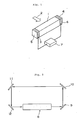
- Fig. 1 is a schematic diagram showing an embodiment of the present invention.
- a medium 1 containing free carriers is an indium antimonide semiconductor measuring 5 x 1 x 1 mm3 and having a carrier density of 1018 cm ⁇ 3. Since the plasma frequency corresponds to a wavelength of about 17 ⁇ m, the device shown in Fig. 1 is suitable for the purpose of amplifying infrared light.
- the medium 1 is placed in a magnetic field 2 having a strength of 0.5 T that is created by a magnetic field applying means (not shown). Placed on opposite ends of the medium 1 are electrodes 3 and 4 which are supplied with a voltage from a power source 7 to produce a carrier accelerating electric field between them.
- the medium 1 is positioned in such a way that the carrier accelerating electric field will cross the magnetic field 2 at right angles.
- Each of the electrodes 3 and 4 is shaped like a ring so that light can pass through its center.
- Another electrodes (not shown are positioned in a direction perpendicular to both the magnetic field 2 and the carrier accelerating electric field and the medium 1 is supplied with a sufficient voltage to cancel the Hall voltage that accompanies carrier drift.
- This electrode may be of a noncontacting type.
- the amplification frequency in the first embodiment is within the far infrared region, so light having a frequency in this range is fed to the medium 1 through the window made in the electrode 3 or 4.
- the polarization plane of this light is selected in such a way that it crosses the magnetic field 2 at right angles.
- amplified output light will be produced from the side opposite to the input side.
- the amplification factor is determined by subtracting an internal loss and a surface reflection from the theoretical value of approximately 30 dB per centimeter. Under a typical condition, an amplification of at least ca. 10 dB per centimeter is expected.
- the gain frequency range may be approximated by the operating theory of the present inventors to lie between ( ⁇ p 2 + ⁇ c 2) 1 ⁇ 2 and 1 ⁇ 2 ⁇ c + ( ⁇ c 2 + 4 ⁇ p 2) 1 ⁇ 2 ⁇ , where ⁇ p and ⁇ c are a plasma angular frequency and a cyclotron angular frequency, respectively. Elsewhere in the present invention, this gain frequency range is simply referred to as the plasma frequency plus or minus the cyclotron frequency.
- indium antimonide is used as the medium 1, but any other material may be used as long as it contains free carriers.
- a preferred example of such alternative materials for the medium 1 is gallium arsenide. If the gallium arsenide crystal is used and if its electron density is 1019 cm ⁇ 3 the gain frequency corresponds to a wavelength of 9 ⁇ m. Indium antimonide and gallium arsenide have large carrier mobility and hence are used advantageously as the material of the medium 1. It should, however, be noted that the material of the medium 1 is by no means limited to these examples and any semiconductors, metals and semimetals may be used by taking into account the above-described limitation on the scattering relaxation time of carriers.
- amplification frequencies in the ultraviolet range may be accomplished with silver or bismuth the plasma frequency of which is within the ultraviolet region.
- the relaxation time of high purity metal can be made conspicuously longer.
- Electron plasma or discharge plasma in low-pressure gases may also be used as the medium 1 and in this case, one only needs to consider electrons while disregarding ions. These plasmas are generally suitable for amplification of microwaves and millimeter waves. Also usable are electron beams. Aside from the problem of the difficulty encountered in insuring the high plasma frequency, electron beams used as the medium 1 feature weaker limitation on the relaxation time because of fewer electron collisions and scattering events within the medium. For circumventing the relaxation time limitation, it is generally effective to hold the medium at low temperatures.
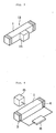
- FIG. 2 A second embodiment of the present invention is described below with reference to Fig. 2.
- An electromagnetic wave device according to this embodiment is designed to function as an oscillator. Shown by 8 in Fig. 2 is the electromagnetic wave device depicted in Fig. 1 and the output light from this device is returned to the input side by means of reflector mirrors 9 - 12.
- the system components shown in Fig. 2 are arranged into a traveling-wave ring structure. In the absence of original input light, the system oscillates on account of its internal gain and supplies an electromagnetic wave having a frequency at the maximum gain. In changing the oscillation frequency of this oscillator, geometrical dimensions such as the distance between the resonator mirrors may be altered simultaneously.
- the oscillation frequency can be altered by frequency modulation which may be effected by changing the plasma frequency, etc.
- the oscillation frequency can be freely changed by various means of frequency modulation.
- the electromagnetic wave device of the present invention does not depend upon fixed particular energy levels, so one of the major features of the device is the wide gain band that can be altered.
- the output electromagnetic wave from the device of the present invention can be modulated by externally modulating such a parameter as changes the frequency band, gain or internal phase shift.
- desired output modulation can be achieved by superposing a modulating component on the applied magnetic field or accelerating electric field which were described as a dc field in the foregoing discussion.
- FIG. 3 shows an electromagnetic wave device according to another embodiment of the present invention which is furnished with means for changing the carrier density. Shown by 13 in Fig. 3 is the electromagnetic wave device depicted in Fig. 1 and shown by 14 is a semiconductor. A pin junction is formed at a boundary between the semiconductor 14 and the medium 1 of the device 13. By applying a voltage to this p-n junction, the density of carriers in the medium 1 can be controlled.
- Fig. 4 shows an electromagnetic device according to a fourth embodiment of the present invention which has a capability of modulating the input electromagnetic wave by means 15 for launching light or fast moving particles into the device. An output signal is obtained in a detector 16 provided in the circuit including electrodes 3 and 4.
- Fig. 5 shows an electromagnetic wave device that makes use of this effect to provide a capability of frequency conversion.
- the device is supplied at the input portion 17 with electromagnetic waves having different frequencies that are produced from two input units. Since no output is produced for frequencies outside the passing band, the embodiment shown in Fig. 5 offers the advantage that a filter for rejecting those frequencies can be omitted.
- Fig. 6 shows an electromagnetic wave device according to a further embodiment of the present invention which has a capability of detecting electromagnetic waves. Shown by 18 and 19 are electrodes that are integral with or independent from the accelerating electrodes 3 and 4 and are combined with a detector 16 to make up means for detecting the electromotive force or current that is generated in the direction of carrier drift.
- the device of the present invention is as a frequency analyzer. If the device is provided with frequency selecting characteristics by either adding a frequency filter such as a resonator to the external circuit or by adjusting various parameters as exemplified above, a series of frequency-analyzed outputs of electromagnetic waves can be obtained by successively changing the characteristics on a time basis.
- a frequency filter such as a resonator
- the electromagnetic device of the present invention consists basically of an amplifier, with a few functional units being added to furnish the device with the ability to work as an oscillator, modulator, frequency converter, detector, etc. depending on the type of added units.
- the electromagnetic waves to be handled by the present invention are within the region determined by the plasma frequency, so it may be operated over the entire range defined by the plasma frequency including not only the region of ordinary electric waves but also the region of light waves or even X-rays.
- the device of the present invention is a unique device available today in that tuning frequencies cover a broad range and that it has the potential to be commercialized as a laser whose operating frequency is in the lightwave region.
- the device of the invention has the great value in its industrial application.
Landscapes
- Physics & Mathematics (AREA)
- Electromagnetism (AREA)
- Engineering & Computer Science (AREA)
- Plasma & Fusion (AREA)
- Optics & Photonics (AREA)
- Plasma Technology (AREA)
- Lasers (AREA)
Applications Claiming Priority (2)
| Application Number | Priority Date | Filing Date | Title |
|---|---|---|---|
| JP215817/88 | 1988-08-30 | ||
| JP63215817A JP2680369B2 (ja) | 1988-08-30 | 1988-08-30 | 電磁波デバイス |
Publications (2)
| Publication Number | Publication Date |
|---|---|
| EP0356941A2 true EP0356941A2 (de) | 1990-03-07 |
| EP0356941A3 EP0356941A3 (de) | 1991-06-05 |
Family
ID=16678749
Family Applications (1)
| Application Number | Title | Priority Date | Filing Date |
|---|---|---|---|
| EP19890115729 Withdrawn EP0356941A3 (de) | 1988-08-30 | 1989-08-25 | Elektromagnetische Wellenvorrichtung |
Country Status (3)
| Country | Link |
|---|---|
| US (1) | US5020064A (de) |
| EP (1) | EP0356941A3 (de) |
| JP (1) | JP2680369B2 (de) |
Cited By (1)
| Publication number | Priority date | Publication date | Assignee | Title |
|---|---|---|---|---|
| WO2000046888A1 (fr) * | 1999-02-02 | 2000-08-10 | Mikhail Arsenovich Ananian | Procede de generation d'un rayonnement et dispositif de mise en oeuvre de ce procede |
Families Citing this family (4)
| Publication number | Priority date | Publication date | Assignee | Title |
|---|---|---|---|---|
| US12356535B2 (en) * | 2018-02-13 | 2025-07-08 | Plasma Futures, Llc | Plasma directed electron beam production of nitric oxide |
| US9601895B2 (en) | 2013-10-18 | 2017-03-21 | Bae Systems Information And Electronic Systems Integration Inc. | Ultra fast semiconductor laser |
| PL414382A1 (pl) | 2015-10-15 | 2017-04-24 | Copernicus Spółka Z Ograniczoną Odpowiedzialnością | Mechanizm nastawczy, w szczególności do dozowania |
| CN113904122A (zh) * | 2021-11-08 | 2022-01-07 | 南京邮电大学 | 一种低损耗及频率可重构型类电磁诱导透明装置 |
Family Cites Families (2)
| Publication number | Priority date | Publication date | Assignee | Title |
|---|---|---|---|---|
| US3292103A (en) * | 1963-03-15 | 1966-12-13 | Jack A Soules | Laser image amplifying system |
| US4727550A (en) * | 1985-09-19 | 1988-02-23 | Chang David B | Radiation source |
-
1988
- 1988-08-30 JP JP63215817A patent/JP2680369B2/ja not_active Expired - Fee Related
-
1989
- 1989-08-14 US US07/393,275 patent/US5020064A/en not_active Expired - Lifetime
- 1989-08-25 EP EP19890115729 patent/EP0356941A3/de not_active Withdrawn
Cited By (2)
| Publication number | Priority date | Publication date | Assignee | Title |
|---|---|---|---|---|
| WO2000046888A1 (fr) * | 1999-02-02 | 2000-08-10 | Mikhail Arsenovich Ananian | Procede de generation d'un rayonnement et dispositif de mise en oeuvre de ce procede |
| RU2159976C2 (ru) * | 1999-02-02 | 2000-11-27 | Автономная некоммерческая организация Институт нанотехнологий Международного фонда конверсии | Способ генерирования излучения и устройство для его осуществления |
Also Published As
| Publication number | Publication date |
|---|---|
| JP2680369B2 (ja) | 1997-11-19 |
| JPH0271578A (ja) | 1990-03-12 |
| US5020064A (en) | 1991-05-28 |
| EP0356941A3 (de) | 1991-06-05 |
Similar Documents
| Publication | Publication Date | Title |
|---|---|---|
| Mork et al. | The modulation response of a semiconductor laser amplifier | |
| Seftor et al. | The electron cyclotron maser as a high-power traveling wave amplifier of millimeter waves | |
| US4063195A (en) | Parametric frequency converter | |
| US5164634A (en) | Electron beam device generating microwave energy via a modulated virtual cathode | |
| Colson et al. | Synchrotron instability for long pulses in free electron laser oscillators | |
| US5020064A (en) | Electromagnetic wave device | |
| Olshansky et al. | Effect of nonlinear gain on the bandwidth of semiconductor lasers | |
| US5043630A (en) | Electron gun with electron beam modulated by an optical device | |
| Savilov | Cyclotron resonance maser with a tapered magnetic field in the regime of “nonresonant” trapping of the electron beam | |
| US3439169A (en) | Tunable solid state laser | |
| Ganguly et al. | Optimization of the efficiency in gyrotron backward‐wave oscillator via a tapered axial magnetic field | |
| US5319322A (en) | Electron beam antenna microwave generation device | |
| Blank et al. | An investigation of X-band gyrotwystron amplifiers | |
| Baird | Survey of fast wave tube developments | |
| US2555150A (en) | Generation of microwave oscillations of stable frequency at high-power levels | |
| Granatstein et al. | Survey of recent gyrotron developments | |
| Lin et al. | Amplification mechanism in the output section of the harmonic multiplying gyrotron traveling-wave amplifier | |
| Seo et al. | A submillimeter Raman free-electron laser in a dense plasma background | |
| Idehara et al. | Mode cooperation in a submillimeter wave FU series gyrotron | |
| US2709786A (en) | Magnetron automatic frequency control | |
| RU2019921C1 (ru) | Многосекционный линейный ускоритель свч | |
| US3076941A (en) | Microwave semiconductive parametric amplifier and multiplier | |
| Kong | Mode-selective amplification in a waveguide free electron laser with a two-sectioned wiggler | |
| Kulke et al. | Small-signal and saturation characteristics of an X-band cyclotron-resonance oscillator | |
| US3657666A (en) | Spin-flip light scattering and gunn effect-type oscillations in multivalley semiconductors subject to a magnetic field |
Legal Events
| Date | Code | Title | Description |
|---|---|---|---|
| PUAI | Public reference made under article 153(3) epc to a published international application that has entered the european phase |
Free format text: ORIGINAL CODE: 0009012 |
|
| AK | Designated contracting states |
Kind code of ref document: A2 Designated state(s): DE GB |
|
| PUAL | Search report despatched |
Free format text: ORIGINAL CODE: 0009013 |
|
| AK | Designated contracting states |
Kind code of ref document: A3 Designated state(s): DE GB |
|
| RHK1 | Main classification (correction) |
Ipc: H01S 3/09 |
|
| 17P | Request for examination filed |
Effective date: 19910701 |
|
| 17Q | First examination report despatched |
Effective date: 19930122 |
|
| APCB | Communication from the board of appeal sent |
Free format text: ORIGINAL CODE: EPIDOS OBAPE |
|
| APCB | Communication from the board of appeal sent |
Free format text: ORIGINAL CODE: EPIDOS OBAPE |
|
| APAB | Appeal dossier modified |
Free format text: ORIGINAL CODE: EPIDOS NOAPE |
|
| STAA | Information on the status of an ep patent application or granted ep patent |
Free format text: STATUS: THE APPLICATION HAS BEEN WITHDRAWN |
|
| 18W | Application withdrawn |
Withdrawal date: 20000717 |
|
| APAF | Appeal reference modified |
Free format text: ORIGINAL CODE: EPIDOSCREFNE |