EP0357202A1 - Verfahren zur Herstellung eines Isolierungsbereichs in einer integrierten Schaltkreisstruktur - Google Patents
Verfahren zur Herstellung eines Isolierungsbereichs in einer integrierten Schaltkreisstruktur Download PDFInfo
- Publication number
- EP0357202A1 EP0357202A1 EP89307286A EP89307286A EP0357202A1 EP 0357202 A1 EP0357202 A1 EP 0357202A1 EP 89307286 A EP89307286 A EP 89307286A EP 89307286 A EP89307286 A EP 89307286A EP 0357202 A1 EP0357202 A1 EP 0357202A1
- Authority
- EP
- European Patent Office
- Prior art keywords
- mask
- slot
- forming
- epitaxial layer
- layer
- Prior art date
- Legal status (The legal status is an assumption and is not a legal conclusion. Google has not performed a legal analysis and makes no representation as to the accuracy of the status listed.)
- Ceased
Links
Images


Classifications
-
- H—ELECTRICITY
- H10—SEMICONDUCTOR DEVICES; ELECTRIC SOLID-STATE DEVICES NOT OTHERWISE PROVIDED FOR
- H10W—GENERIC PACKAGES, INTERCONNECTIONS, CONNECTORS OR OTHER CONSTRUCTIONAL DETAILS OF DEVICES COVERED BY CLASS H10
- H10W10/00—Isolation regions in semiconductor bodies between components of integrated devices
- H10W10/01—Manufacture or treatment
- H10W10/011—Manufacture or treatment of isolation regions comprising dielectric materials
- H10W10/014—Manufacture or treatment of isolation regions comprising dielectric materials using trench refilling with dielectric materials, e.g. shallow trench isolations
- H10W10/0142—Manufacture or treatment of isolation regions comprising dielectric materials using trench refilling with dielectric materials, e.g. shallow trench isolations the dielectric materials being chemical transformed from non-dielectric materials
-
- H—ELECTRICITY
- H10—SEMICONDUCTOR DEVICES; ELECTRIC SOLID-STATE DEVICES NOT OTHERWISE PROVIDED FOR
- H10W—GENERIC PACKAGES, INTERCONNECTIONS, CONNECTORS OR OTHER CONSTRUCTIONAL DETAILS OF DEVICES COVERED BY CLASS H10
- H10W10/00—Isolation regions in semiconductor bodies between components of integrated devices
- H10W10/10—Isolation regions comprising dielectric materials
- H10W10/17—Isolation regions comprising dielectric materials formed using trench refilling with dielectric materials, e.g. shallow trench isolations
Definitions
- This invention relates to the formation of an isolation region in the substrate of an integrated circuit structure. More particularly, this invention relates to a method for forming such an isolation region in which a layer of epitaxially grown material is formed over an isolation slot formed in the substrate of an integrated circuit structure, thereby eliminating the need for a separate step to refill the slot after the slot walls have been oxidized.
- isolation regions are formed to electrically isolate and insulate adjacent active devices, or components, from one another.
- One such method for forming such isolation regions involves the formation of a slot or groove in a substrate. The walls of this slot or groove are then oxidized, to form the desired isolation or insulation, followed by refilling of the slot, usually with oxide or polysilicon. The surface of the structure is then planarized using wet or dry etching techniques and/or mechanical polishing.
- damage to the substrate may occur due to stresses formed by excessive oxide growth in the slot.
- the substrate may also be stressed by void formation during refilling with polysilicon as a result of opening the void during subsequent planarization followed by oxidation of the sidewalls of the void. Formation of an oxide cap on the slot, in a manner wherein the oxide grows down into the slot, can also create stress.
- Mechanical polishing of the structure during planarization after refill may break the wafers, or leave refill material on the backside of the wafers which may also warp the wafers.
- an isolation region in the substrate of an integrated circuit structure wherein an epitaxial layer is grown over an isolation slot formed in the substrate and lined with oxide prior to the growth of the epitaxial layer and the epitaxial layer is then selectively etched to thin the layer in the region where the isolation slot is formed followed by selective oxidation of the thinned portion of the layer down to the level of the substrate so that the oxide formed by oxidation of the thinned epitaxial layer is contiguous with the oxide on the sidewalls of the isolation slot.
- the drawings illustrate an improved method for forming an isolation region in the substrate of an integrated circuit structure wherein an isolation slot, formed in a substrate and lined with oxide to provide the desired isolation/insulation between active devices or components in the structure, is either filled or covered by growing an epitaxial layer over the structure.
- the epitaxial layer is then patterned and the portion of the layer over the isolation slot is then oxidized to provide an oxide cap over the slot without extending the oxide growth into the slot to thereby avoid creating stresses in the substrate.
- the portion of the epitaxial layer overlying the isolation slot is first thinned prior to oxidation thereof to facilitate oxidizing the remaining portions of the thinned epitaxial layer down to the level of the oxidized sidewalls of the isolation slot.
- a silicon substrate 10 is shown with an optional buried layer 12 formed thereon which may serve as the buried collector layer of a bipolar device.
- a buried layer may be formed by initially masking substrate 10 to only expose portions of the substrate to be doped to form buried layer 12. Since the formation of such a buried layer is only optional and forms no part of the present invention, the remaining figures will denote the substrate and any buried layer formed therein collectively by the numeral 10.
- the substrate is prepared for formation of an isolation slot or region by first cleaning the substrate surface, e.g., with a 10:1 water/HF solution, and then growing or depositing, over substrate 10, a thin oxide layer 20 having a thickness of approximately 350-600 Angstroms ( ⁇ ) to provide a compatible interface between the surface of silicon substrate 10 and a nitride masking layer to be applied.
- first cleaning the substrate surface e.g., with a 10:1 water/HF solution
- a thin oxide layer 20 having a thickness of approximately 350-600 Angstroms ( ⁇ ) to provide a compatible interface between the surface of silicon substrate 10 and a nitride masking layer to be applied.
- a nitride layer 30 is then deposited over oxide layer 20 to a thickness of from about 1000 to about 1500 ⁇ , preferably about 1200 ⁇ , and a layer 40 of glass, e.g., silicon oxide, is then deposited to a thickness of from about 1 to 1.5 microns (10-15K ⁇ ).
- Glass layer 40 may be undoped or may be doped with from about 4-6 wt.% phosphorus, for purposes of convenience if a later phosphorus-doped topside (passivation) glass layer is used over the finished structure (since the same apparatus may then be used to form both layers).
- a photoresist mask 50 is then applied over the structure and patterned to form an opening 54, as shown in Figure 2, conforming to the desired width of the isolation slot to be formed in substrate 10.
- Glass layer 40, nitride layer 30, and oxide layer 20 are then etched through mask opening 54 in resist mask layer 50 using plasma or RIE etching to form opening 44.
- Resist layer 50 is normally then removed prior to etching the isolation slot in silicon substrate 10, to prevent formation of carbon deposits in the slot during the silicon slot etch, leaving the oxide/nitride/oxide slot mask formed from layers 20, 30, and 40 as shown in Figure 3.
- Slot 14 is then etched in substrate 10 through the mask opening in layers 20, 30, and 40 to a depth which may be from about 4 to about 7 microns for a bipolar devices or as little as 1 micron for MOS devices using, for example, a RIE etching system to etch the silicon as shown in Figure 4. It will be noted that the lower level of optional buried layer 12 is shown by a dotted line 13 in Figure 4 to illustrate that to achieve the desired isolation, the depth of slot 14 should exceed the thickness of any buried layer previously formed in substrate 10.
- a slot channel stop region 16 may be implanted into substrate 10 at the bottom of slot 14 by implantation of, for example, boron at an energy level of, for example, about 60 kEV for a P-type substrate, or phosphorus at a similarly appropriate energy level for an N-type substrate, through the slot mask opening in layers 2, 30, and 40 to prevent any possibilities of inversion in the substrate during operation of active devices subsequently formed thereon.
- glass layer 40 and any oxide in slot 14 may be removed using a hydrogen-fluoride etchant solution, stopping on the underlying nitride mask layer 30.
- Damaged silicon, in the substrate walls of slot 14 may then be removed using a silicon etch solution such as a mixture of CrO3 + HF or NH4OH + H2O2. It should be noted that this step may be carried out, if desired, prior to implantation of channel stop region 16 in substrate 10 at the bottom of slot 14.
- a silicon etch solution such as a mixture of CrO3 + HF or NH4OH + H2O2. It should be noted that this step may be carried out, if desired, prior to implantation of channel stop region 16 in substrate 10 at the bottom of slot 14.
- the exposed silicon walls of slot 14 are oxidized to provide an oxide layer or coating 60 of from about 2000 to about 3000 ⁇ as shown in Figure 5.
- Oxide coating 60 may be formed by CVD, bu preferivelyably is grown by exposing the structure to a steam atmosphere for about 10 minutes at a temperature of from about 1000 to about 1100°C.
- oxide coating 60 on the walls of slot 14 the structure is subjected to a brief, i.e., 10-15 second, wet etch, such as 10:1 HF, or its derivative, ammonium fluoride + HF, to remove any oxide remaining on nitride layer 30 followed by a phosphoric acid etch to remove nitride layer 40, and a further oxide removal etch to remove oxide layer 20 beneath nitride layer 30, resulting in the structure shown in Figure 6.
- wet etch such as 10:1 HF, or its derivative, ammonium fluoride + HF
- oxide coating 60 is predetermined or preselected to be sufficient to provide for the removal or loss of some oxide during the etching steps to remove the nitride and oxide slot mask layers remaining on the structure, while leaving a sufficient amount to provide the desired isolation or insulation, i.e., at least around 800 ⁇ .
- a layer 70 of epitaxial silicon is now grown over the silicon substrate after removal of oxide layer 20, which, in the embodiment shown in Figure 7, also fills slot 14 at 70a.
- Epitaxial silicon layer 70 is grown over substrate 10 to a depth or thickness of from about 1 to 2 microns, depending upon the width of slot 14 as well as the desired thickness of epitaxial layer 70 over those regions of the substrate where active devices will eventually be constructed.
- epitaxial layer 70 is preferably doped by including a doping agent such as arsenic, for N-type epitaxial silicon, or boron, for P-type epitaxial silicon, in the silane gas used for such epitaxial growth. If it is considered not desirable to fill slot 14 with such doped epitaxial silicon, the epitaxial growth optionally may be divided into two steps or stages with about 0.3 to 0.5 microns of undoped epitaxial silicon first grown, followed by the remainder of the epitaxial silicon grown in the presence of the dopant.
- a doping agent such as arsenic, for N-type epitaxial silicon, or boron, for P-type epitaxial silicon
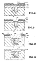
- epitaxial silicon layer 70 After growth of epitaxial silicon layer 70, the entire surface of epitaxial layer 70 may be oxidized to form an oxide mask layer 80 which provides a compatible surface on which a nitride mask layer 90 may be applied.
- a photoresist mask layer 100 may then be applied having an oversized opening 104 therein which generally defines an area of substrate 10 which will not be used for the construction of active devices and which will, preferably, completely cover the area defined by slot 14, including the oxide coating 60 on the walls of slot 14, and also overlap a portion of substrate 10 around slot 14 as well, as illustrated in Figure 8.
- opening 94 which exposes the underlying surface of epitaxial silicon layer 70.
- the exposed area of epitaxial silicon layer 70 is preferably etched to thin the thickness down so that it can be completely oxidized down to the underlying isolation slot.
- the amount of epitaxial silicon removed should be a sufficient amount of the original thickness of the epitaxial silicon layer so that subsequent oxidation of the remaining epitaxial silicon will result in a complete filling with oxide of the opening created by removal of the epitaxial silicon. This oxide filling will occur since oxidation results in upward as well as downward growth of the oxide because silicon oxide occupies a larger volume than the silicon from which it is formed by the oxidation.
- the amount of epitaxial silicon removed by such a thinning step will also vary with the original thickness of the epitaxial layer. For example, if a 2 micron epitaxial layer is formed, the epitaxial layer should be thinned by removing from about 1 to about 1.5 microns while a 1 micron thick epitaxial layer may be thinned an amount ranging from 0 to about 0.5 microns to leave behind, in either case, a thickness of epitaxial silicon over the isolation slot of from about 0.5 to about 1 micron.
- the structure is exposed to an oxidizing atmosphere until all of the exposed epitaxial silicon has been oxidized to form an oxide cap 110 over slot 14 which extends at least down to the level of oxide 60 on the side walls of slot 14, resulting in the structure shown in Figure 10.
- This may be done by exposing the structure to an oxidizing medium such as warm steam, for a period of approximately 4-5 hours at about 1000°C, or by using a high pressure oxidation process.
- oxide cap 110 is shown actually extending down further than the height of oxide layer 60 and slightly into substrate 10 in the exposed area immediately adjacent isolation slot 14 (the original buried layer area prior to diffusion into the epitaxial layer if a buried layer is present). While oxide cap 110 need not actually extend this far into substrate 10, it is important that oxide cap 110 extend down far enough so that oxide cap 110 is contiguous with oxide 60 to provide the desired isolation. A slight over extension of oxide cap downward into substrate 10 will assure the contiguity of oxide cap 110 with oxide 60 without, however, resulting in the creation of stress in the substrate as when prior art oxide is grown in the slot itself to provide the oxide cap.
- oxidation of the non-device area of epitaxial layer 70 down to substrate 10, or to the buried layer in the substrate can have advantages such as reducing the base storage area in lateral PNP devices, resulting in a speed up of the device.
- oxide cap 110 may result in the formation of "bird's beak" regions 114 of oxide laterally adjacent to oxide cap 110 due to some oxidation of the covered portions of epitaxial layer 70 beneath mask layers 80 and 90, as shown in Figure 10. Since epitaxial layer 70 is thicker in this area, much of the "bird's beak” regions 114 will extend upwardly of the final upper surface of oxide cap 110.
- oxide 114 lends itself to optional removal of much of the undesirable oxide growth 114 by a simple planarization step in which a planarizing layer of photoresist material may be applied over the surface of oxide cap 110, oxide regions 114 and the remainder of the surface of epitaxial layer 70, after removal of oxide mask layer 80 and nitride mask layer 90, and the surface RIE etched or mechanically polished to remove the oxide regions 114.
- an isolation slot prior to the formation of the epitaxial layer, in which the oxidized slot is either then refilled with epitaxial silicon up to the level of the epitaxial layer formed during such refilling of the isolation slot, or else covered with the epitaxial layer, followed by local oxidation of the area of the epitaxial layer over the slot down to the level of the oxidized walls of the slot results in the formation of an isolation slot with an oxide cap thereon wherein formation of stresses in the adjacent substrate have been substantially eliminated by virtue of the formation of the oxide cap above the level of the substrate.
Landscapes
- Element Separation (AREA)
Applications Claiming Priority (2)
| Application Number | Priority Date | Filing Date | Title |
|---|---|---|---|
| US211835 | 1988-06-27 | ||
| US24183588A | 1988-09-06 | 1988-09-06 |
Publications (1)
| Publication Number | Publication Date |
|---|---|
| EP0357202A1 true EP0357202A1 (de) | 1990-03-07 |
Family
ID=22912371
Family Applications (1)
| Application Number | Title | Priority Date | Filing Date |
|---|---|---|---|
| EP89307286A Ceased EP0357202A1 (de) | 1988-08-12 | 1989-07-19 | Verfahren zur Herstellung eines Isolierungsbereichs in einer integrierten Schaltkreisstruktur |
Country Status (1)
| Country | Link |
|---|---|
| EP (1) | EP0357202A1 (de) |
Citations (2)
| Publication number | Priority date | Publication date | Assignee | Title |
|---|---|---|---|---|
| US4546538A (en) * | 1983-09-05 | 1985-10-15 | Oki Electric Industry Co., Ltd. | Method of manufacturing semiconductor integrated circuit devices having dielectric isolation regions |
| EP0263756A2 (de) * | 1986-10-06 | 1988-04-13 | Fairchild Semiconductor Corporation | Verwendung einer selektiven Epitaxie für BiCMOS-Verfahren |
-
1989
- 1989-07-19 EP EP89307286A patent/EP0357202A1/de not_active Ceased
Patent Citations (2)
| Publication number | Priority date | Publication date | Assignee | Title |
|---|---|---|---|---|
| US4546538A (en) * | 1983-09-05 | 1985-10-15 | Oki Electric Industry Co., Ltd. | Method of manufacturing semiconductor integrated circuit devices having dielectric isolation regions |
| EP0263756A2 (de) * | 1986-10-06 | 1988-04-13 | Fairchild Semiconductor Corporation | Verwendung einer selektiven Epitaxie für BiCMOS-Verfahren |
Non-Patent Citations (1)
| Title |
|---|
| EXTENDED ABSTRACTS, vol. 86-2, 19th-24th October 1986, pages 407-408, Princeton, NJ, US; A. WITKOWSKI et al.: "Device isolation using selective-epi field-oxidation (SEL-FOX)" * |
Similar Documents
| Publication | Publication Date | Title |
|---|---|---|
| KR960016502B1 (ko) | 집적 회로 분리 방법 | |
| US7994605B2 (en) | Isolation structure for semiconductor integrated circuit substrate | |
| EP0181188B1 (de) | Verfahren zur Herstellung von Gräben in integrierten Schaltungen | |
| US6967146B2 (en) | Isolation region forming methods | |
| US6737330B2 (en) | Isolation structure and fabricating method therefor | |
| US6518147B1 (en) | Process for manufacturing an SOI wafer by oxidation of buried channels | |
| US4541167A (en) | Method for integrated circuit device isolation | |
| US5728620A (en) | Isolation method of semiconductor device | |
| US4853344A (en) | Method of integrated circuit isolation oxidizing walls of isolation slot, growing expitaxial layer over isolation slot, and oxidizing epitaxial layer over isolation slot | |
| US5972776A (en) | Method of forming a planar isolation structure in an integrated circuit | |
| EP0068275B1 (de) | Verfahren zur Herstellung von Halbleiteranordnungen mittels reaktiven Ionenätzens | |
| US5371036A (en) | Locos technology with narrow silicon trench | |
| JP3363420B2 (ja) | 自己整合トレンチを有するパターン付きシリコン・オン・インシュレータ基板の製造方法 | |
| US5192706A (en) | Method for semiconductor isolation | |
| US5252511A (en) | Isolation method in a semiconductor device | |
| US5877067A (en) | Method of manufacturing a semiconductor device | |
| EP0357202A1 (de) | Verfahren zur Herstellung eines Isolierungsbereichs in einer integrierten Schaltkreisstruktur | |
| JP3719854B2 (ja) | 半導体装置の製造方法 | |
| US6261966B1 (en) | Method for improving trench isolation | |
| JPH07183370A (ja) | 半導体装置の製造方法 | |
| EP0137195A1 (de) | Dielektrisch isolierte Schaltung und Verfahren zur Herstellung | |
| JPH0521592A (ja) | 半導体装置の製造方法及び半導体装置 | |
| US6436831B1 (en) | Methods of forming insulative plugs and oxide plug forming methods | |
| US20030064597A1 (en) | Method of semiconductor device isolation |
Legal Events
| Date | Code | Title | Description |
|---|---|---|---|
| PUAI | Public reference made under article 153(3) epc to a published international application that has entered the european phase |
Free format text: ORIGINAL CODE: 0009012 |
|
| AK | Designated contracting states |
Kind code of ref document: A1 Designated state(s): AT BE CH DE ES FR GB GR IT LI LU NL SE |
|
| 17P | Request for examination filed |
Effective date: 19900405 |
|
| 17Q | First examination report despatched |
Effective date: 19921023 |
|
| GRAG | Despatch of communication of intention to grant |
Free format text: ORIGINAL CODE: EPIDOS AGRA |
|
| STAA | Information on the status of an ep patent application or granted ep patent |
Free format text: STATUS: THE APPLICATION HAS BEEN REFUSED |
|
| 18R | Application refused |
Effective date: 19970405 |