EP0357233A2 - Wellenleitergerät - Google Patents
Wellenleitergerät Download PDFInfo
- Publication number
- EP0357233A2 EP0357233A2 EP89307818A EP89307818A EP0357233A2 EP 0357233 A2 EP0357233 A2 EP 0357233A2 EP 89307818 A EP89307818 A EP 89307818A EP 89307818 A EP89307818 A EP 89307818A EP 0357233 A2 EP0357233 A2 EP 0357233A2
- Authority
- EP
- European Patent Office
- Prior art keywords
- waveguide
- slots
- portions
- extensive
- waveguide apparatus
- Prior art date
- Legal status (The legal status is an assumption and is not a legal conclusion. Google has not performed a legal analysis and makes no representation as to the accuracy of the status listed.)
- Withdrawn
Links
Images

Classifications
-
- H—ELECTRICITY
- H01—ELECTRIC ELEMENTS
- H01P—WAVEGUIDES; RESONATORS, LINES, OR OTHER DEVICES OF THE WAVEGUIDE TYPE
- H01P11/00—Apparatus or processes specially adapted for manufacturing waveguides or resonators, lines, or other devices of the waveguide type
- H01P11/001—Manufacturing waveguides or transmission lines of the waveguide type
- H01P11/002—Manufacturing hollow waveguides
-
- H—ELECTRICITY
- H01—ELECTRIC ELEMENTS
- H01P—WAVEGUIDES; RESONATORS, LINES, OR OTHER DEVICES OF THE WAVEGUIDE TYPE
- H01P3/00—Waveguides; Transmission lines of the waveguide type
- H01P3/12—Hollow waveguides
-
- H—ELECTRICITY
- H01—ELECTRIC ELEMENTS
- H01Q—ANTENNAS, i.e. RADIO AERIALS
- H01Q21/00—Antenna arrays or systems
- H01Q21/0006—Particular feeding systems
- H01Q21/0037—Particular feeding systems linear waveguide fed arrays
- H01Q21/0043—Slotted waveguides
Definitions
- This invention relates to waveguide apparatus and in particular, but not exclusively, to apparatus comprising a waveguide consisting of two or more sections.
- E-plane technology With the advent of modern transceiver/receiver technology, often operating at millimetre wavelengths, it is sometimes necessary to use what is commonly referred to as E-plane technology.
- E-plane technology refers to the technique of mounting devices in the E-plane or electric field plane of the dominant mode of the waveguide. This plane usually extends along the waveguide perpendicular to the broadwall of the waveguide at the position where the radio frequency current is a minimum, normally in the plane bisecting the broadwall.
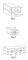
- the dielectric substrate 5 normally in the form of a PCB, is located in detents 6 in the waveguide 7. As the substrate does not extend across the whole width of the waveguide walls there is thus a continuous inner metallic wall and therefore no escape path for the signal being propagated along the waveguide.
- this technique requires precise machining of the guide and substrate and leads to problems in connecting components carried by the substrate to apparatus outside the waveguide.
- the dielectric substrate 8 may have components mounted on it prior to assembly which can be connected via conductors carried by the substrate to the external wall 9. Construction tolerances are not so critical, as the substrate is simply sandwiched between the sections 10 and 11 of the waveguide, and can therefore be produced more cheaply than the apparatus shown in Figure 2.
- the substrate extends into secondary cavities 13 and 14 on either side of the waveguide. These behave as radio frequency chokes limiting power losses from the central cavity 12. However, there may still be an appreciable power loss from the waveguide and the bulk of th structure is considerably increased.
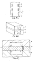
- Slots 15 are incorporated within the dielectric 17 separated by gaps d as shown in Figure 4A. These slots 15 are through-plated so as to have a conductive layer 16 on their inner surfaces.
- the inner conductive surfaces 16 of the slots 15 bridge the gap between the sections 18 and 19. This effectively continues the metallic wall of the waveguide across the dielectric region 17, except in the regions of the gaps between adjacent slots, d , which still permit some power loss from the guide.
- the present invention arose as a result of attempting to reduce further these power losses. further these power losses.
- waveguide apparatus comprising a waveguide having partly sandwiched in one or more walls of the waveguide a dielectric substrate characterised in that the substrate incorporates a plurality of slots, each comprising a first elongate portion having extensive to one side from both ends, second and third elongate portions, each slot having a conductive layer upon at least part of its inner surface, being of substantially the same orientation as its neighbours, first portions of adjacent slots being substantially co-linear, and part at least of the conductive surface of the slots being so positioned as to form part of the inner surface of the waveguide.
- the dielectric substrate when suitably located, enables E-plane technology to be employed and permits components to be mounted on the dielectric prior to assembly.
- the conductive coatings on the inner surfaces of the slots effectively form a continuation of the inner metallic wall across the thickness of the dielectric, parallel to the wall of the waveguide which the dielectric intersects, and controls the power losses.
- the power losses through the regions between the slots, where there is no conductive material, are controlled by the second and third elongate portions of the slots, which can be arranged so that the region between adjacent slots function as waveguides.
- the coupling factor can be controlled. This is a measure of the ratio of coupling between the field within the waveguide cavity and that outside the waveguide, and is dependent upon: the width of the gap between the second portion of each slot and the third portion of the adjacent slot; the angle between these second and third portions; the length of said second and third portions; the thickness of the substrate and the value of the dielectric constant of the substrate material. It is therefore possible, by selecting suitable dimensions and configurations of the slots, to control the coupling factor and accurately control power losses through the gaps.
- Attenuation of the waveguide is to be optimised it is preferable to have waveguide apparatus wherein the slots are arranged so as to minimise power losses from the waveguide.
- Arranging the apparatus in this manner providing long narrow gaps between the slots perpendicular to the waveguide, causes high attenuation in these areas by acting as a waveguide with a cut-off frequency below that of the wave being propagated along the main waveguide cavity. This therefore greatly reduces losses, whilst still providing an electrically non-conductive structure for supporting components within the waveguide which is of sufficient strength for assembly purposes and which is physically robust.
- the waveguide apparatus in which the configuration of slots is arranged such that the waveguide apparatus functions as an antenna, that is, in which, rather than reducing losses, it is arranged so that radiation escapes from the waveguide in a controlled fashion.
- the second and third portions of the adjacent slots are arranged non-parallel to each other and have a minimum separation at their ends adjoining the first portions.
- the arrangement of the slots in this manner enables accurate control of power losses through each gap, and angling said second and third portions enables each gap to effectively act as a two-dimensional horned antenna.
- the positioning and dimensions of the slots may be accurately achieved, for example, by stamping, use of the invention enables millimetric wave array antennas to be fabricated more cheaply and easily than has previously been possible.
- most production techniques for producing such antennas involve expensive CNC machining of slots in a waveguide body, but at millimetric wavelengths it is difficult to achieve the required tolerances which may make prediction of radiation levels difficult.
- an electrical component is arranged to connect conductive layers extensive from facing walls of the waveguide, enabling modification of a signal transmitted along the waveguide to be achieved.
- a plurality of said components are included to control the phase and/or amplitude of a signal as it is transmitted along the waveguide.
- the waveguide may thus be arranged to act as an active phased array antenna.
- Construction of a phased array antenna in the above manner offers considerable advantages over conventional construction techniques already described and enables appropriate components to be sub-assembled upon the substrate prior to assembly within the waveguide itself, providing a very efficient way of manufacturing compact steerable phased array antennas.
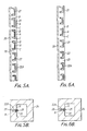
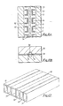
- a dielectric substrate 20 for use in waveguide apparatus and shown shaded for reasons of clarity, has slots 21 in it.
- Each slot has three portions A, B and C, which correspond to first, second and third portions respectively.
- the slots 21 are linearly arranged with the first portions A of adjacent slots being substantially co-linear.
- the second and third portions B and C of each slot are arranged at right angles to the first portion A.
- Each slot has a metallised inner surface 22 which is continuous with a metallic area 22A on one of the surfaces of the dielectric substrate 20.
- This substrate 20 is shown assembled within a waveguide 24 in Figure 5B, the metallised area 22A being extensive within the waveguide to form a finline waveguide.
- This illustrated arrangement has lower power losses than a conventional finline waveguide because the portions B and C of the slots are extensive from portion A in a direction away from the central cavity of the waveguide 24.
- the metallised coating 22 of the end portions B and C causes the gaps 23 betwen adjacent slots to function as waveguides, the dimensions being such that the cut-off frequency of the gap is less than that of the signal being propagated, causing attentation of the wave in the gaps 23 and thereby reducing losses from the waveguide 24 itself.
- Broken lines indicate the location of different parts of the substrate 20 illustrated in Figure 5A when it is positioned in the waveguide 24.
- adjacent slots 21 in a dielectric substrate 20 are more widely spaced than those in the substrate of Figure 5A, enabling the regions 23 between slots to act as propagation paths for the signal.
- the waveguide apparatus in Figure 6B which incorporates the substrate 20 of Figures 6A, functions as a phased array antenna. The size of the gap between the slots 21 is determined empirically.
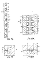
- the waveguide apparatus When the substrate 20 is incorporated in the waveguide 24, as shown in Figure 7B, the waveguide apparatus functions as a horned phased array antenna, permitting energy to be radiated through the gaps 23 between the slots 21.
- FIG. 8A another dielectric substrate 25 is shown, which includes two parallel rows 26 and 27 of slots. Each slot is similar to those illustrated in Figure 5A, and the two rows 26 and 27 are arranged so that the second and third portions B and C of one row of slots extend from the corresponding first portions A in the opposite direction to those of the other row. Each slot is covered with a metallic layer 28 on its inner surface. There are also two metallised areas 29 and 30 which surround the slots on the upper surface as shown of the dielectric substrate 25.
- Figure 8B shows the substrate 25 of Figure 8A located within a waveguide 31 which is formed from two sections 32 and 33. The metallised coating 28 on the slot surfaces effectively extends the waveguide inner wall 34 across the boundary between the two sections 32 and 33.
- the portions B and C of the slots function as described with reference to Figures 5A and 5B.
- the portions B and C of the slots in both rows 26 and 27 are extensive from portion A in a direction away from the central cavity 35 of the waveguide 31.
- the metallised coating 28 of the end portion B and C causes the gaps 36 betwen adjacent slots to function as waveguides, the dimensions being such that the cut-off frequency of the gap is less than that of the signal being propagated causing attenuation of the wave in the gaps 36 and thereby reducing losses from the waveguide 31 itself.
- the metallised areas 29 and 30 are extensive within the central cavity 35 of the waveguide 31, its extent being indicated by the broken lines, and functions as a fin-line waveguide.
- the waveguide apparatus is arranged to act as a phased array antenna.
- Figure 9 schematically shows a conventional slotted array antenna. It comprises a waveguide 37 having slots 38 machined in it, these slots usually being produced by expensive CNC machining techniques not capable of producing the tolerances required for millimetric systems as are possible using the present invention.
- Figures 10A and 10B schematically show a phased array antenna in accordance with the present invention.
- Figure 10A illustrates in plan view a dielectric substrate 39 having two rows 40 and 41 of s1ots through it.
- the lower row 40 is designed to reduce losses from the waveguide to a minimum, the first portion A of the slots being as long as practicable and the gaps 42 between adjacent slots the minimum possible whilst ensuring that the substrate 39 is physically robust enough for assembly purposes and to withstand physical shocks it is likely to receive in service.
- the narrow gaps 42 between the slots allow very little radiation to escape from the waveguide.
- the slots of the upper row 41 are arranged to have a substantially wider gap 43 between adjacent slots.
- the second and third portions are angled with respect to the first portions so as to form what are effectively two-dimensional antenna horns between adjacent slots. This enables radiation to escape from the waveguide in a controlled manner.
- a component 44 is mounted between two conductive areas 45 and 46 surrounding the slots, and may be a PIN diode or other such device to enable the phase and/or amplitude of a signal travelling along the guide to be modified. Although only one component is shown, in practical applications there would be many such components.
- the substrate 39 is assembled in the waveguide 47 as shown in Figure 10B, where two such substrates have been incorporated, one row 40 of slots limits radiation from the bottom section of the waveguide 47 whilst the other row 41 of slots permits radiation to escape from the waveguide through its upper face.
- the component 44 (not shown in Figure 10B) is used to control the phase and/or amplitude of the signal in the waveguide, enabling the waveguide apparatus to act as a steerable phased array antenna.
- Insulating layers 48 shown in Figure 10B, enable a potential difference to be applied between two regions 49 and 50 of the waveguide 47 thereby providing a potential difference between the metallised areas 45 and 46 of Figure 8A. This provides a potential difference across component 44 and therefore a means of controlling the component.
- a dielectric substrate 51 includes two rows 52 and 53 of slots arranged to reduce power losses from a waveguide.
- Each slot is filled with conductive material 54, which, when the substrate 51 is located in a waveguide 55, forms part of the inner surface of the waveguide wall, as shown in Figure 11B.
- the slots are set back from the waveguide cavity 56 so that the effective inner surface of the waveguide is indented.
- Figure 12 shows a rectangular array antenna consisting of sectons of waveguide apparatus 57, 58 and 59, each of which is similar to the waveguide apparatus shown in Figures 10B, but having only a single dielectric layer 60.
- the input signal to all the guides may be applied to them in parallel, and the phase of the waves in each section may be controlled such that a steerable array may be produced.
Landscapes
- Engineering & Computer Science (AREA)
- Manufacturing & Machinery (AREA)
- Variable-Direction Aerials And Aerial Arrays (AREA)
- Waveguide Aerials (AREA)
- Waveguides (AREA)
Applications Claiming Priority (2)
| Application Number | Priority Date | Filing Date | Title |
|---|---|---|---|
| GB8820526A GB2209354B (en) | 1987-08-31 | 1988-08-31 | Filter medium forming system and process |
| GB8820556 | 1988-08-31 |
Publications (2)
| Publication Number | Publication Date |
|---|---|
| EP0357233A2 true EP0357233A2 (de) | 1990-03-07 |
| EP0357233A3 EP0357233A3 (de) | 1990-08-29 |
Family
ID=10642914
Family Applications (1)
| Application Number | Title | Priority Date | Filing Date |
|---|---|---|---|
| EP89307818A Withdrawn EP0357233A3 (de) | 1988-08-31 | 1989-08-01 | Wellenleitergerät |
Country Status (1)
| Country | Link |
|---|---|
| EP (1) | EP0357233A3 (de) |
Cited By (1)
| Publication number | Priority date | Publication date | Assignee | Title |
|---|---|---|---|---|
| EP2553758A4 (de) * | 2010-03-31 | 2014-05-28 | Hewlett Packard Development Co | Wellenleitersystem und verfahren dafür |
Family Cites Families (5)
| Publication number | Priority date | Publication date | Assignee | Title |
|---|---|---|---|---|
| US3031666A (en) * | 1955-06-06 | 1962-04-24 | Sanders Associates Inc | Three conductor planar antenna |
| FR1210710A (fr) * | 1958-06-04 | 1960-03-10 | Thomson Houston Comp Francaise | Nouvelle fenêtre étanche pour guides d'ondes |
| BE772078A (fr) * | 1971-03-19 | 1972-01-17 | Thomson Csf | Coupleurs en hyperfrequence a paroi metallique mince |
| US4052683A (en) * | 1974-02-28 | 1977-10-04 | U.S. Philips Corporation | Microwave device |
| AU5669886A (en) * | 1985-10-03 | 1987-04-24 | Allied Corporation | Waveguide slot array antenna |
-
1989
- 1989-08-01 EP EP89307818A patent/EP0357233A3/de not_active Withdrawn
Cited By (2)
| Publication number | Priority date | Publication date | Assignee | Title |
|---|---|---|---|---|
| EP2553758A4 (de) * | 2010-03-31 | 2014-05-28 | Hewlett Packard Development Co | Wellenleitersystem und verfahren dafür |
| US9014526B2 (en) | 2010-03-31 | 2015-04-21 | Hewlett-Packard Development Company, L.P. | Waveguide system and methods |
Also Published As
| Publication number | Publication date |
|---|---|
| EP0357233A3 (de) | 1990-08-29 |
Similar Documents
| Publication | Publication Date | Title |
|---|---|---|
| US11626652B2 (en) | Ridge gap waveguide and multilayer antenna array including the same | |
| US4500887A (en) | Microstrip notch antenna | |
| EP3621146B1 (de) | Hochfrequenzfilter und phasengesteuerte gruppenantenne mit solch einem hochfrequenzfilter | |
| US4689584A (en) | Dielectric slab circulators | |
| EP0985243B1 (de) | Vorrichtung zur mikrowellenübertragung | |
| KR101089195B1 (ko) | 유전체 도파관의 입출력 결합 구조 | |
| EP1398848B1 (de) | Geschichtete Aperturantenne und damit ausgestattete mehrschichtige Leiterplatte | |
| KR20000017029A (ko) | 다층 세라믹 기판을 사용하여 형성된 안테나 | |
| JPH0671171B2 (ja) | 広帯域アンテナ | |
| KR20020061106A (ko) | 전송 선로, 집적회로 및 송수신 장치 | |
| US20200119423A1 (en) | Connection structure between waveguide and coaxial cable | |
| US4970522A (en) | Waveguide apparatus | |
| KR100744209B1 (ko) | 삼각형 일체형 전송 구조물 | |
| AU676114B2 (en) | End launched microstrip (or stripline)to waveguide transition using a cavity backed slot fed by a t-shaped microstrip line | |
| US5724049A (en) | End launched microstrip or stripline to waveguide transition with cavity backed slot fed by offset microstrip line usable in a missile | |
| US3277489A (en) | Millimeter phased array | |
| KR930008831B1 (ko) | 동축-마이크로스트립 직교런처 | |
| WO1986003891A2 (en) | A compound dielectric multi-conductor transmission line and devices constructed therefrom | |
| KR100836967B1 (ko) | 다채널 도파관 구조물 | |
| EP0357233A2 (de) | Wellenleitergerät | |
| KR20050058477A (ko) | 선로 변환기, 고주파 모듈 및 통신 장치 | |
| US4338609A (en) | Short horn radiator assembly | |
| CA1157938A (en) | Line source antenna for electronic beam scanning | |
| JPH03254209A (ja) | 軸スロット筒状アンテナ | |
| US3594812A (en) | Strip line ferrite phase shifter |
Legal Events
| Date | Code | Title | Description |
|---|---|---|---|
| PUAI | Public reference made under article 153(3) epc to a published international application that has entered the european phase |
Free format text: ORIGINAL CODE: 0009012 |
|
| AK | Designated contracting states |
Kind code of ref document: A2 Designated state(s): AT BE CH DE ES FR GR IT LI LU NL SE |
|
| PUAL | Search report despatched |
Free format text: ORIGINAL CODE: 0009013 |
|
| AK | Designated contracting states |
Kind code of ref document: A3 Designated state(s): AT BE CH DE ES FR GR IT LI LU NL SE |
|
| 17P | Request for examination filed |
Effective date: 19901012 |
|
| STAA | Information on the status of an ep patent application or granted ep patent |
Free format text: STATUS: THE APPLICATION IS DEEMED TO BE WITHDRAWN |
|
| 18D | Application deemed to be withdrawn |
Effective date: 19920303 |