EP0357265A2 - Nichtlinearer Resonanzschalter und Konverter - Google Patents
Nichtlinearer Resonanzschalter und Konverter Download PDFInfo
- Publication number
- EP0357265A2 EP0357265A2 EP89308098A EP89308098A EP0357265A2 EP 0357265 A2 EP0357265 A2 EP 0357265A2 EP 89308098 A EP89308098 A EP 89308098A EP 89308098 A EP89308098 A EP 89308098A EP 0357265 A2 EP0357265 A2 EP 0357265A2
- Authority
- EP
- European Patent Office
- Prior art keywords
- switch
- current
- nonlinear
- resonant
- capacitor
- Prior art date
- Legal status (The legal status is an assumption and is not a legal conclusion. Google has not performed a legal analysis and makes no representation as to the accuracy of the status listed.)
- Ceased
Links
Images


Classifications
-
- H—ELECTRICITY
- H03—ELECTRONIC CIRCUITRY
- H03K—PULSE TECHNIQUE
- H03K17/00—Electronic switching or gating, i.e. not by contact-making and –breaking
-
- H—ELECTRICITY
- H02—GENERATION; CONVERSION OR DISTRIBUTION OF ELECTRIC POWER
- H02M—APPARATUS FOR CONVERSION BETWEEN AC AND AC, BETWEEN AC AND DC, OR BETWEEN DC AND DC, AND FOR USE WITH MAINS OR SIMILAR POWER SUPPLY SYSTEMS; CONVERSION OF DC OR AC INPUT POWER INTO SURGE OUTPUT POWER; CONTROL OR REGULATION THEREOF
- H02M3/00—Conversion of DC power input into DC power output
- H02M3/02—Conversion of DC power input into DC power output without intermediate conversion into AC
- H02M3/04—Conversion of DC power input into DC power output without intermediate conversion into AC by static converters
- H02M3/10—Conversion of DC power input into DC power output without intermediate conversion into AC by static converters using discharge tubes with control electrode or semiconductor devices with control electrode
- H02M3/145—Conversion of DC power input into DC power output without intermediate conversion into AC by static converters using discharge tubes with control electrode or semiconductor devices with control electrode using devices of a triode or transistor type requiring continuous application of a control signal
- H02M3/155—Conversion of DC power input into DC power output without intermediate conversion into AC by static converters using discharge tubes with control electrode or semiconductor devices with control electrode using devices of a triode or transistor type requiring continuous application of a control signal using semiconductor devices only
Definitions
- This invention relates to resonant switches and particularly to nonlinear resonant switches useful in power conversion devices and to converters using such switches.
- US Patent No. 4,415,959 discloses a DC-to-DC converter with a switching device connected in series with a source of energy and an LC circuit effecting current pulses through the switch.
- a control circuit turns the switch on and off when the current is zero, thus eliminating switching losses.
- pulse-width-modulated (PWM) converters of various kinds can be adapted to resonant switch operation to achieve zero current switching and therefore realize no switching losses.
- PWM pulse-width-modulated
- previously proposed resonant switch converters have the disadvantage that, for the same output current and power, resonant quasi-sinusoidal waveforms exhibit higher peak values than do the rectangular waveforms of conventional pulse-width-modulated converters. Consequently, resonant switch converters exhibit higher conduction losses in the transistor and these increased conduction losses can partially or wholly negate the gains made by the elimination of switching losses.
- power FET'S have desirable characteristics for switching in power conversion devices, they do have significant resistance. Thus it is important to minimize the peak current to minimize the losses.
- a nonlinear resonant switch and a nonlinear resonant switch converter in accordance with the present invention are characterised by the features specified in the characterising portions of Claims 1 and 7 respectively.
- a nonlinear resonant switch comprising a nonlinear reactor having a magnetic core with a primary winding and a secondary winding on the magnetic core; saturating means for saturating the magnetic core at low primary winding currents and permitting unsaturation at high primary winding currents; a primary circuit comprising a semiconductor switch means serially connected with a resonant tank circuit, the resonant tank circuit including the said primary winding and a capacitor, whereby the peak tank circuit current is attenuated by the inductance of the nonlinear reactor in its unsaturated condition; timing means for timing the switching of the semiconductor switch means with respect to the tank resonance to switch when current through the semiconductor switch means is zero, thereby optimizing switching efficiency; a diode combined with the capacitor in parallel; and a secondary circuit comprising the diode and capacitor combination in series with the secondary winding.
- the invention is further carried out by a converter utilizing a nonlinear resonant switch in accordance with the present invention.
- the nonlinear resonant switch described here combines the zero current switching of previous resonant switch schemes with the low peak currents of conventional pulse-width-modulated converters.
- a nonlinear tank circuit is devised with ringing current distorted such that the peak value is reduced.
- Transistor switching still occurs at zero current but the peak current need only be 10% to 20% greater than that of the conventional PWM converter.
- Such a waveform can be obtained by use of a controlled saturation inductor.
- the nonlinear resonant concept is quite general and can be applied to a wide variety of resonant and quasi-resonant linear topologies.
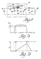
- Figure 1 depicts a general case of a resonant nonlinear switch 10 as applied to a buck converter configuration.
- Input terminals 12 are connected across a voltage supply 14 and output terminals 16 are connected to an LC filter, comprising filter inductor 18 and capacitor 19 and a load 20.
- a switch element 22 semiconductor switch means arranged for either half-wave or full-wave operation is connected in series with linear tank elements, inductor L1 (or 24) and capacitor C (or 26), and a nonlinear inductance L2 (or 28).
- the nonlinear inductance comprises a primary winding 28 on a magnetic core 30 having a secondary winding 32 and a turns ratio N.
- the turns ratio N generally determines the value of the peak current.
- the secondary winding 32 is coupled at one end to one output terminal 16 and at the other end through a diode 36 to the other output terminal 16.
- the diode 36 is also in parallel with the capacitor 26.
- an auxiliary winding 34 is included to bias the magnetic core 30 toward saturation.
- the primary winding 28, secondary winding 32, magnetic core 30 define a non-linear reactor.
- the saturation of the magnetic core 30 is determined by a core bias circuit 38 and the current in the secondary winding 32.
- the core bias circuit 38 provides a constant DC current to the auxiliary winding 34 sufficient, in combination with the secondary winding current, to bias the magnetic core 30 to saturation in the presence of small primary winding currents.
- the bias is overcome, however, by large primary currents which produce flux opposing that of the bias and secondary winding currents to drive the magnetic core 30 into unsaturated condition.
- Figure 2 is a graph of the core flux vs. primary or switch current (Ig) for an idealized core. The flux is constant until the primary current reaches a critical value I c indicating core saturation.
- FIG. 3 graphs the total tank inductance against the tank current for an idealized magnetic core.
- the circuit is designed with the nonlinear inductance L2 (unsaturated) much larger than the combined inductance L1 and nonlinear inductance L2 (saturated).
- the combined inductance increases dramatically when the secondary current passes the critical value I c .
- the inductance may increase, for example, by a factor of one hundred to one thousand.
- the linear inductor L1 may also be omitted; the tank inductance for small primary current is then the saturated value of L2.
- Secondary winding 32, auxiliary winding 34 and core bias circuit 38 thereby define saturating means.
- the core bias circuit 38 and auxiliary winding 34 are not essential to the core saturation scheme.
- Another way to achieve the desired core saturation characteristics described above is to control the output current (I f ) in the secondary winding to a substantially constant value to provide the desired degree of saturation.
- the output filter stage When used in conjunction with a converter, the output filter stage has a large filter inductor 18 in series with the secondary winding 32 which maintains the secondary current at a stable amplitude.
- the nonlinear inductance L2 is biased by the output current I f such that it is saturated at low current but is not saturated at high current (in the vicinity of NI f - Figure 2), this has the effect of limiting the peak tank current to approximately N times I f .
- the turns ratio N is chosen to be slightly greater than unity so that the peak switch current is only slightly greater than in the conventional PWM switched mode case.
- L1 is chosen to limit the rate of rise of switch current to a level which yields acceptably low switching losses.
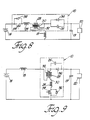
- the feedback switch control 40 (timing means) which is coupled to the tank circuit to sense the current flowing through the switch element 22.
- the feedback switch control 40 includes a VCO 42 for setting a switching frequency, a latch 44 comprising a pair of cross coupled NAND gates 46 and 48, a zero crossing detector 50 sensing the tank current to provide a signal when the current is zero, and a transistor driver 52 to turn the switch element 22 on and off.
- the VCO 42 is connected to an input of NAND gate 46 (the set input) and the zero crossing detector 50 is connected to an input of NAND gate 48 (the reset input).
- the output voltages of the VCO 42 and the zero crossing detector 50 are normally high and momentarily go low to set or reset the latch 44.
- the switch element 22 which normally comprises a transistor coupled to a diode, is turned on by the VCO signal and turned off by the zero crossing detector signal. In each event, the current through the switch element 22 is zero.
- the VCO frequency must be set low enough by a control voltage input to assure that the tank current returns to zero prior to turning the switch on. In the case of a half-wave converter a single pulse of tank current is allowed before turning the switch off. For a full-wave converter, two or more pulses are passed for each switch on period.
- the switch element 22 for a half-wave buck converter is a power FET 54 in series with a diode 56.
- the full-wave buck converter circuit shown in Figure 6, uses a power FET 54 with a counter parallel diode 56 to allow conduction in the direction opposite to the transistor current. In each case, the core bias circuit 38 and the feedback switch control 40 are assumed, though not shown.
- the power FET 54 has just switched on and the switch current increases at a rate limited by the total saturated tank inductance while the capacitance voltage V c remains at zero since the diode 36 is conducting.
- the diode 36 becomes backbiased and the capacitance voltage V c begins to increase.
- the switch current I g increases at a progressively lower rate since the voltage across the inductances L1 and L2 is decreasing. Thus far the magnetic core 30 has been saturated.
- the switch current I g reaches the critical level I c where it is sufficient to overcome the core bias and the magnetic core 30 becomes unsaturated.
- the very high inductance of the tank circuit during this period prevents rapid current changes so that the switch current waveform has a gently rounded top rather than a high sinusoidal peak typical of a tank circuit oscillation.
- the capacitance 26 steadily charges during this period.
- the switching current I g decreases and reaches the critical value I c
- the magnetic core 30 again saturates at the beginning of the interval 4 and the low inductance allows the switch current Ig to decrease rapidly to zero.
- the capacitor 26 discharges to zero volts and during interval 6, the diode 36 conducts to accommodate the output current maintained by the (filter) inductor 18.
- the non-linear inductance L2 was wound on a Magnetics Inc. 1408-G material ungapped ferrite pot core, with 12 turns #24 AWG primary and 15 turns #26 AWG secondary for a turns ratio N of 1.25.
- the inductor 24 consisted of 6 turns of #20 AWG copper wire on a Magnetics, Inc.
- FIG 8 is a schematic diagram of a buck-boost nonlinear resonant switch converter.
- the switch configuration is the same as for Figure 6.
- the converter circuit differences are that the filter inductor 18 is connected to the negative side of the voltage supply 14 and the tank circuit is connected to the positive side of the load 20 and capacitor 19.
- the primary loop includes the voltage supply 14, switch element (power FET and diode 54, 56), inductor 24, primary winding 28, the tank circuit (capacitor and diode 26, 36) and the capacitor 19 and load 20.
- the secondary loop comprises the filter inductor 18, the secondary winding 32, the tank circuit (capacitor and diode 26, 36) and the capacitor 19 and load 20.
- Figure 9 shows the circuit for a boost-type nonlinear resonant switch converter.
- the filter inductor 18 is serially connected between the voltage supply 14 and the secondary winding 32.
- the secondary loop comprises the voltage supply 14, the filter inductor 18, the secondary winding 32, the tank circuit (capacitor and diode 26, 36), and the capacitor 19 and load 20.
- the primary loop includes the switch element (power FET and diode 54, 56), inductor 24, primary winding 28, the tank circuit (capacitor and diode 26, 36) and the capacitor 19 and load 20.
- the converters disclosed herein have in common a nonlinear resonant switch wherein the nonlinear element is an inductor biased to saturation for low switch currents and to nonsaturation for high switch currents.
- the primary loop of the converter includes the primary winding in series with a switch element, a tank circuit and an energy device comprising either the voltage supply 14 or a capacitor 19, or both.
- the secondary loop includes the secondary winding in series with a filter inductor and one of the energy devices. Both loops share the tank circuit capacitor 26 which is in parallel with a diode 36.
- the switch is controlled to switch on and off when the tank current is zero and the core bias is controlled by the secondary winding or by a bias circuit and a separate winding.
- the nonlinear resonant switch converter For the nonlinear resonant switch converter the following is required: (1) insert the nonlinear inductor primary winding effectively in series with the transistor switch, (2) insert a diode effectively in series (half-wave) or counter parallel (full-wave) with the transistor switch, (3) insert the nonlinear inductor secondary winding effectively in series with the filter inductor of the PWM converter, (4) insert a tank capacitor effectively in parallel with the original converter diode, and (5) modify the control circuit to ensure zero current switching.
- An auxiliary bias circuit may be added. If the PWM converter contains multiple filter inductors, then additional nonlinear inductor secondary windings may be necessary so that the peak switch current is maintained at 10% to 20% greater than that of the original PWM converter.
Landscapes
- Engineering & Computer Science (AREA)
- Power Engineering (AREA)
- Dc-Dc Converters (AREA)
Applications Claiming Priority (2)
| Application Number | Priority Date | Filing Date | Title |
|---|---|---|---|
| US07/239,812 US4829232A (en) | 1988-09-02 | 1988-09-02 | Nonlinear resonant switch and converter |
| US239812 | 1988-09-02 |
Publications (2)
| Publication Number | Publication Date |
|---|---|
| EP0357265A2 true EP0357265A2 (de) | 1990-03-07 |
| EP0357265A3 EP0357265A3 (de) | 1990-12-27 |
Family
ID=22903849
Family Applications (1)
| Application Number | Title | Priority Date | Filing Date |
|---|---|---|---|
| EP19890308098 Ceased EP0357265A3 (de) | 1988-09-02 | 1989-08-09 | Nichtlinearer Resonanzschalter und Konverter |
Country Status (5)
| Country | Link |
|---|---|
| US (1) | US4829232A (de) |
| EP (1) | EP0357265A3 (de) |
| JP (1) | JPH02111258A (de) |
| KR (1) | KR930000966B1 (de) |
| CA (1) | CA1290809C (de) |
Cited By (2)
| Publication number | Priority date | Publication date | Assignee | Title |
|---|---|---|---|---|
| EP0568123A1 (de) * | 1992-04-02 | 1993-11-03 | Philips Patentverwaltung GmbH | Verlustarme Stromversorgungseinrichtung mit einem Gleichspannungswandler |
| CN111312301A (zh) * | 2018-12-12 | 2020-06-19 | 北京兆易创新科技股份有限公司 | 一种控制偏置电流的电路 |
Families Citing this family (15)
| Publication number | Priority date | Publication date | Assignee | Title |
|---|---|---|---|---|
| DE3842465A1 (de) * | 1988-12-16 | 1990-06-28 | Flachenecker Gerhard | Schaltregler zur gleichspannungswandlung |
| US5132890A (en) * | 1991-01-09 | 1992-07-21 | Koss Corporation | Power supply based on normally parasitic resistance of solid state switch |
| US5321348A (en) * | 1991-03-08 | 1994-06-14 | Vlt Corporation | Boost switching power conversion |
| US5432431A (en) * | 1992-05-21 | 1995-07-11 | Vlt Corporation | Boost switching power conversion using saturable inductors |
| US5583424A (en) * | 1993-03-15 | 1996-12-10 | Kabushiki Kaisha Toshiba | Magnetic element for power supply and dc-to-dc converter |
| US5572417A (en) * | 1994-07-13 | 1996-11-05 | Vlt Corporation | AC to DC boost power converters |
| US5659460A (en) * | 1994-11-03 | 1997-08-19 | Vlt Corporation | Switch control in quantized power converters |
| US5663635A (en) * | 1995-05-24 | 1997-09-02 | Vlt Corporation | Reverse energy transfer in zero-current switching power conversion |
| US6255635B1 (en) | 1998-07-10 | 2001-07-03 | Ameritherm, Inc. | System and method for providing RF power to a load |
| KR100359072B1 (ko) * | 2000-08-25 | 2002-10-31 | 삼성전기주식회사 | 과전류 방지 기능을 갖는 트랜스의 공진회로 |
| US6472852B1 (en) * | 2000-11-02 | 2002-10-29 | Semtech Corporation | Resonant buck-type voltage converter using swinging inductance |
| US6693805B1 (en) * | 2002-07-31 | 2004-02-17 | Lockheed Martin Corporation | Ripple cancellation circuit for ultra-low-noise power supplies |
| JP3861220B2 (ja) * | 2004-06-24 | 2006-12-20 | ミネベア株式会社 | Dc−dcコンバータ |
| WO2009114873A1 (en) | 2008-03-14 | 2009-09-17 | Volterra Semiconductor Corporation | Voltage converter inductor having a nonlinear inductance value |
| US9979273B2 (en) | 2016-05-19 | 2018-05-22 | Abb Schweiz Ag | Resonant converters with variable inductor |
Family Cites Families (7)
| Publication number | Priority date | Publication date | Assignee | Title |
|---|---|---|---|---|
| US3663949A (en) * | 1970-11-30 | 1972-05-16 | Bose Corp | Current sensing of indicator current in series with transformer winding |
| US4187458A (en) * | 1978-08-07 | 1980-02-05 | The United States Of America As Represented By The Secretary Of The Army | Constant power regenerative magnetic switching regulator |
| US4415959A (en) * | 1981-03-20 | 1983-11-15 | Vicor Corporation | Forward converter switching at zero current |
| US4415962A (en) * | 1981-06-15 | 1983-11-15 | Massachusetts Institute Of Technology | Current mode sine wave inverter |
| FR2528256A1 (fr) * | 1982-06-07 | 1983-12-09 | Signaux Entr Electriques | Convertisseur d'alimentation a decoupage |
| GB2126806B (en) * | 1982-06-30 | 1985-11-06 | Fenner Co Ltd J H | Chopper circuit |
| US4591966A (en) * | 1983-05-19 | 1986-05-27 | Steve Smith | Rectifying network |
-
1988
- 1988-09-02 US US07/239,812 patent/US4829232A/en not_active Expired - Lifetime
-
1989
- 1989-05-24 CA CA000600493A patent/CA1290809C/en not_active Expired - Lifetime
- 1989-08-09 EP EP19890308098 patent/EP0357265A3/de not_active Ceased
- 1989-09-01 KR KR1019890012641A patent/KR930000966B1/ko not_active Expired - Fee Related
- 1989-09-01 JP JP1227311A patent/JPH02111258A/ja active Granted
Cited By (3)
| Publication number | Priority date | Publication date | Assignee | Title |
|---|---|---|---|---|
| EP0568123A1 (de) * | 1992-04-02 | 1993-11-03 | Philips Patentverwaltung GmbH | Verlustarme Stromversorgungseinrichtung mit einem Gleichspannungswandler |
| CN111312301A (zh) * | 2018-12-12 | 2020-06-19 | 北京兆易创新科技股份有限公司 | 一种控制偏置电流的电路 |
| CN111312301B (zh) * | 2018-12-12 | 2022-02-11 | 北京兆易创新科技股份有限公司 | 一种控制偏置电流的电路 |
Also Published As
| Publication number | Publication date |
|---|---|
| CA1290809C (en) | 1991-10-15 |
| EP0357265A3 (de) | 1990-12-27 |
| KR900005698A (ko) | 1990-04-14 |
| US4829232A (en) | 1989-05-09 |
| JPH0586144B2 (de) | 1993-12-10 |
| JPH02111258A (ja) | 1990-04-24 |
| KR930000966B1 (ko) | 1993-02-11 |
Similar Documents
| Publication | Publication Date | Title |
|---|---|---|
| EP0357265A2 (de) | Nichtlinearer Resonanzschalter und Konverter | |
| US4866367A (en) | Multi-loop control for quasi-resonant converters | |
| US5508903A (en) | Interleaved DC to DC flyback converters with reduced current and voltage stresses | |
| US5418703A (en) | DC-DC converter with reset control for enhanced zero-volt switching | |
| JP3199423B2 (ja) | 共振形フォワードコンバ−タ | |
| US7019988B2 (en) | Switching-type power converter | |
| US5293111A (en) | Method for minimizing the switching loss in a power switch | |
| US5172308A (en) | DC-DC converter with transformer having a single secondary winding | |
| US4417153A (en) | High frequency switching circuit | |
| US6198644B1 (en) | Rectifying/smoothing circuit and double-ended converter | |
| JP3494154B2 (ja) | パワートランジスタの駆動用電源回路 | |
| EP0534422B1 (de) | Stromversorgungsvorrichtung | |
| EP0925638B1 (de) | Dc/dc - umrichterschaltung | |
| Agrawal et al. | Capacitor voltage clamped series resonant power supply with improved cross regulation | |
| WO2002015371A2 (en) | Switched magamp post regulator | |
| US4538219A (en) | Multiwinding inductor and associated apparatus | |
| US5257170A (en) | Electric converter with several induction coils | |
| GB2233479A (en) | Regulated DC-DC power supply | |
| JP2737391B2 (ja) | リンギングチョークコンバータ | |
| Harada et al. | Saturable inductor commutation for zero voltage switching in DC-DC converter | |
| KR950001294Y1 (ko) | 클램프회로가 내장된 영(zero)전압 스위칭 다중공진 컨버터 | |
| EP1490959A1 (de) | Ein leistungswandler | |
| JPH0739149A (ja) | 電圧共振コンバータ用整流平滑回路 | |
| Martiš et al. | 12 kW Flyback Converter with a Passive Quasi-resonant Snubber | |
| SU1742956A1 (ru) | Двухканальный преобразователь посто нного напр жени |
Legal Events
| Date | Code | Title | Description |
|---|---|---|---|
| PUAI | Public reference made under article 153(3) epc to a published international application that has entered the european phase |
Free format text: ORIGINAL CODE: 0009012 |
|
| AK | Designated contracting states |
Kind code of ref document: A2 Designated state(s): DE FR GB IT |
|
| PUAL | Search report despatched |
Free format text: ORIGINAL CODE: 0009013 |
|
| AK | Designated contracting states |
Kind code of ref document: A3 Designated state(s): DE FR GB IT |
|
| 17P | Request for examination filed |
Effective date: 19910221 |
|
| 17Q | First examination report despatched |
Effective date: 19930212 |
|
| STAA | Information on the status of an ep patent application or granted ep patent |
Free format text: STATUS: THE APPLICATION HAS BEEN REFUSED |
|
| 18R | Application refused |
Effective date: 19940214 |