EP0357448B1 - Alimentations électriques de puissance - Google Patents
Alimentations électriques de puissance Download PDFInfo
- Publication number
- EP0357448B1 EP0357448B1 EP19890308867 EP89308867A EP0357448B1 EP 0357448 B1 EP0357448 B1 EP 0357448B1 EP 19890308867 EP19890308867 EP 19890308867 EP 89308867 A EP89308867 A EP 89308867A EP 0357448 B1 EP0357448 B1 EP 0357448B1
- Authority
- EP
- European Patent Office
- Prior art keywords
- power output
- output terminal
- electrical power
- fault
- fault condition
- Prior art date
- Legal status (The legal status is an assumption and is not a legal conclusion. Google has not performed a legal analysis and makes no representation as to the accuracy of the status listed.)
- Expired - Lifetime
Links
- 238000004804 winding Methods 0.000 claims description 51
- 230000008878 coupling Effects 0.000 claims description 14
- 238000010168 coupling process Methods 0.000 claims description 14
- 238000005859 coupling reaction Methods 0.000 claims description 14
- 230000004044 response Effects 0.000 claims description 9
- 238000000034 method Methods 0.000 claims description 4
- 238000012544 monitoring process Methods 0.000 claims description 4
- 239000003990 capacitor Substances 0.000 description 7
- 239000004065 semiconductor Substances 0.000 description 6
- 230000001105 regulatory effect Effects 0.000 description 4
- 230000007423 decrease Effects 0.000 description 3
- 230000001419 dependent effect Effects 0.000 description 3
- 238000010586 diagram Methods 0.000 description 2
- 230000015654 memory Effects 0.000 description 2
- 238000007639 printing Methods 0.000 description 2
- XUIMIQQOPSSXEZ-UHFFFAOYSA-N Silicon Chemical compound [Si] XUIMIQQOPSSXEZ-UHFFFAOYSA-N 0.000 description 1
- 230000005611 electricity Effects 0.000 description 1
- 238000004146 energy storage Methods 0.000 description 1
- 230000006870 function Effects 0.000 description 1
- 230000007246 mechanism Effects 0.000 description 1
- 238000013021 overheating Methods 0.000 description 1
- 229910052710 silicon Inorganic materials 0.000 description 1
- 239000010703 silicon Substances 0.000 description 1
Images


Classifications
-
- H—ELECTRICITY
- H02—GENERATION; CONVERSION OR DISTRIBUTION OF ELECTRIC POWER
- H02H—EMERGENCY PROTECTIVE CIRCUIT ARRANGEMENTS
- H02H3/00—Emergency protective circuit arrangements for automatic disconnection directly responsive to an undesired change from normal electric working condition with or without subsequent reconnection ; integrated protection
- H02H3/20—Emergency protective circuit arrangements for automatic disconnection directly responsive to an undesired change from normal electric working condition with or without subsequent reconnection ; integrated protection responsive to excess voltage
- H02H3/207—Emergency protective circuit arrangements for automatic disconnection directly responsive to an undesired change from normal electric working condition with or without subsequent reconnection ; integrated protection responsive to excess voltage also responsive to under-voltage
-
- H—ELECTRICITY
- H02—GENERATION; CONVERSION OR DISTRIBUTION OF ELECTRIC POWER
- H02M—APPARATUS FOR CONVERSION BETWEEN AC AND AC, BETWEEN AC AND DC, OR BETWEEN DC AND DC, AND FOR USE WITH MAINS OR SIMILAR POWER SUPPLY SYSTEMS; CONVERSION OF DC OR AC INPUT POWER INTO SURGE OUTPUT POWER; CONTROL OR REGULATION THEREOF
- H02M3/00—Conversion of DC power input into DC power output
- H02M3/22—Conversion of DC power input into DC power output with intermediate conversion into AC
- H02M3/24—Conversion of DC power input into DC power output with intermediate conversion into AC by static converters
- H02M3/28—Conversion of DC power input into DC power output with intermediate conversion into AC by static converters using discharge tubes with control electrode or semiconductor devices with control electrode to produce the intermediate AC
- H02M3/325—Conversion of DC power input into DC power output with intermediate conversion into AC by static converters using discharge tubes with control electrode or semiconductor devices with control electrode to produce the intermediate AC using devices of a triode or a transistor type requiring continuous application of a control signal
- H02M3/335—Conversion of DC power input into DC power output with intermediate conversion into AC by static converters using discharge tubes with control electrode or semiconductor devices with control electrode to produce the intermediate AC using devices of a triode or a transistor type requiring continuous application of a control signal using semiconductor devices only
Definitions
- This invention relates to power supplies and in particular to power supply circuits for energising electronic circuits of franking machines and incorporating means for monitoring over and under-voltage conditions of the power supply output.
- US 3,327,128 relates to apparatus for protecting load circuitry supplied by a power supply having a plurality of output supplies.
- US 3,327,128 discloses an electrical power supply in which the outputs from two secondary windings of a transformer are independently rectified and regulated to provide power to load circuitry.
- the output connection from each of the secondary windings includes a relay winding which, in the event of an excess current condition in that output, closes a contact to connect an excess load to the other output such that there is an excess current condition in the other output also.
- the excess current overloading of the electrical power outputs from both secondary windings causes a fuse in the primary circuit to blow.
- an electrical power supply including a transformer having a primary winding for input of electrical power, a first secondary winding and a second secondary winding; said first and second secondary windings being electromagnetically coupled to said primary winding for energisation by the electrical power input to the primary winding; first and second power output terminals to receive electrical power output from said first and second secondary windings respectively; a fault detector connected to said first power output terminal operative in responsive to a first fault condition at said first power output terminal to cause termination of electrical power input to the primary winding; and a coupling from the second power output terminal to the first power output terminal effective upon occurrence of a second fault condition at said second power output terminal to produce the first fault condition at the first power output terminal to cause operation of the fault detector is characterised by electromagnetic coupling in said transformer between the first and second secondary windings of the transformer, said electromagnetic coupling between said first and second secondary windings solely being effective upon occurrence of the second fault condition at the second power output terminal to produce the first fault condition at the first power output terminal
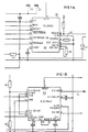
- Figure 1 is a circuit diagram of a switch mode power supply incorporating over and under-voltage monitoring in accordance with the invention
- Figure 2 is a block diagram illustrating the use of the power supply to provide power to a franking machine.
- a 23V AC power input is obtained from a mains electricity supply by means of a transformer (not shown) and is applied to terminals 20, 21.
- This power input is applied through a temperature sensing fuse 22 and a fusible resistor 23, connected in series, to a bridge rectifier 24.
- the fusible resistor 23 serves to limit the inrush of current when the AC power is applied to the circuit.
- a voltage dependent resistor 25 is connected across the input to the bridge rectifier, the resistor having a characteristic such that its resistance decreases with increasing voltage across the resistor. Therefore if an excessive voltage is applied to the terminals 20, 21, the voltage dependent resistor goes to a low resistance state thereby increasing the current flow through the fusible resistor 23 and causing that resistor to fuse and go open circuit.
- the temperature sensing fuse is fitted when it is desired to provide evidence of any overheating of the circuits.
- a negative output terminal 26 of the bridge rectifier 24 is connected to a ground line 27.
- a positive output terminal 28 is connected through a fuse 29 and rectifier 30 to provide an unregulated DC supply to a switch mode power module 31.
- a reservoir capacitor 32 and a capacitor 33, providing a low impedance at very high frequency are connected between the unregulated DC supply and ground.
- the switch mode power module is a switching pulse width modulated regulator circuit comprising a semi-conductor circuit component 34 driving an electromagnetic energy storage component 35.
- the electromagnetic component 35 consists of a primary winding 36 electromagnetically coupled to a feedback secondary winding 37 and a further secondary winding 38.
- the semi-conductor circuit component 34 includes an oscillator, a preregulator/start-up circuit, a precision voltage reference, a current mode controller and a MOSFET switching transistor.
- the component includes over-current protection and under-voltage lockout.
- a commercially available component is a type No. S.I. 9100 marketed by Siliconix.
- the switching frequency is determined by resistor 39, connected between pins numbered 7 and 8 of the component, and is nominally 100kHz. Current pulses are fed to the primary winding 36 at the switching frequency which is substantially uniform but the pulses have a variable width or duration which is dependent upon the energy drawn from the module 31.
- a resistor 40 sets the maximum magnitude of current permitted to flow in the primary winding 36. If the current exceeds this maximum magnitude internal control circuits in the semi-conductor component 34 operate to shut down the module 31.
- One end of the feedback winding 37 is connected to ground while the other end is connected through a rectifier diode 41, a potential divider consisting of resistors 42, 43 and a series resistor 44 to a feedback input terminal pin number 14 of the semi-conductor component 34.
- the resistance of the resistors 42, 43 is chosen such that the voltage at the junction between the diode 41 and the resistor 42 is maintained at 10v and this voltage is utilised to supply power to various devices requiring power at this voltage of 10v on line 45.
- One end of the secondary winding 38 is connected to ground while the other end is connected through a rectifier diode 46 to an input of a low drop-out voltage regulator 47.
- a suitable component is type no. L4805 marketed by SGS.
- a reservoir capacitor 48 is connected between the input 50 of voltage regulator 47 and ground.
- by-pass capacitors 49 are connected between the input 50 of voltage regulator and ground and between an output 51 of the regulator 47 and ground.
- the regulator 47 provides a regulated 5v supply at the output 51.
- a monitor circuit comprising a semi-conductor circuit component 52 is provided to detect any over-voltage condition arising on the regulated 5v supply at the output 51.
- a suitable semi-conductor component is type No. S.G. 3543 marketed by Silicon General. Such over-voltage conditions may arise due to faults in the power supply circuit or due to the deliberate application of excessive voltage to the circuits of the franking machine in a fraudulent attempt to misuse the franking machine.
- the regulated 5v supply is connected to the component 52 to power the component on pin number 16 and in addition a potential divider comprising resistors 53, 54 applies a proportion of the 5v supply to an over-voltage sense input pin number 6 of the component 52.
- a trigger signal is output on pin number 1 to trip a voltage controlled rectifier or thyristor 55 which is connected from the junction 56 of fuse 29 and rectifier 30 to ground 27.
- thyristor 55 When thyristor 55 is tripped it presents a very low resistance or short circuit and causes the fuse 29 to blow. As a result power input is removed from the switch mode power supply module 31 and the circuits of the franking machine are no longer powered.
- the circuit component 52 also monitors the output of the bridge rectifier 24 to detect any failure of the power input.
- the junction 56 of the fuse 29 and rectifier 30 is connected by line 57 through a potential divider comprising resistors 58, 59 to a further terminal pin number 10 of the component 52.
- the rectifier 30 is provided to isolate the reservoir capacitor 32 from the line 57.
- the monitor circuit can detect a failure of power input immediately without any delay which otherwise would occur due to waiting for the capacitor 32 to discharge.
- a battery 60 is connected through an isolating rectifier 61 to the input of the voltage regulator 47.
- the unregulated input to the voltage regulator 47 is monitored by the monitor component 52 by a connection through a potential divider comprising resistors 62, 63 to an under-voltage sense input terminal pin number 7 of component 52.
- the monitor In the event that the voltage at the input to the regulator 47 falls below a predetermined magnitude, the monitor outputs a signal on terminal pin number 9 which is connected to a microprocessor of the franking machine circuits to assert a reset of the processor circuits.
- a franking machine comprises a microprocessor 64 which performs accounting and control functions, a keyboard 65 for input of data to the microprocessor, a display 66 for the display of data, memories 67 for storing accounting data generated by the microprocessor relating to usage of the franking machine and a printing device such as a print drum 68 for the printing of franking impressions on mail items.
- the print drum 68 includes selectively settable print elements such as print wheels to enable different values of franking to be printed.
- the print wheels are set to the selected value by means 69 comprising setting mechanisms driven by electric motors.
- the value of franking printed by the drum 68 is controlled by the microprocessor 64 by selective operation of the motors of the means 69 in dependence upon a selected value of franking input to the microprocessor by means of the keyboard.
- the components of the franking machine are powered by means of the power supply 70 described hereinbefore with reference to Figure 1.
- the 5v output on line 51 is utilised to power the electronic components including the microprocessor 64, keyboard 65, display 66 and memories 67 and the 10v supply on line 45 is utilised to power the electric motors of the print element setting means 69.
- the output on pin 9 of the monitor 52 generated in the event of the voltage input to the regulator 47 falling below a predetermined magnitude, is connected by means of line 71 to a reset input of the microprocessor to cause a reset of the microprocessor circuits to occur.
- any fraudulent attempt to misuse the franking machine by application of voltages above those normally present during operation of the machine may result in the application of excessive voltage not only to the 5v supply on output 51 but also to the 10v supply on output 43. Accordingly it is required that this output also be monitored for over-voltage conditions. Clearly this could be accomplished by providing an additional monitor circuit. However this is undesirable not only from the additional cost but also from the space occupied by any such additional circuit.
- the feedback winding 37 of the transformer 35 from which the 10v supply is obtained is electromagnetically coupled to the secondary winding 38 from which the 5v supply is obtained.
- the voltage output of the secondary winding 38 increases.
- the current drawn from the 10v supply decreases the voltage output of the winding 38 decreases. Therefore should a fault in the loading of the 10v supply on output 43 occur, it is reflected to the 5v supply and is detected by the monitor circuit 52.
Landscapes
- Engineering & Computer Science (AREA)
- Power Engineering (AREA)
- Dc-Dc Converters (AREA)
- Emergency Protection Circuit Devices (AREA)
- Protection Of Static Devices (AREA)
Claims (9)
- Alimentation de puissance électrique comprenant un transformateur (35) comportant un enroulement primaire (36) pour l'entrée de puissance électrique, un premier enroulement secondaire (37) et un second enroulement secondaire (38) ; le premier et le second enroulement secondaire (37, 38) étant couplés électromagnétiquement à l'enroulement primaire (36) pour être excités par la puissance électrique d'entrée de l'enroulement primaire ; une première et une seconde borne de sortie de puissance (45, 50) pour recevoir respectivement la puissance de sortie électrique du premier et du second enroulement secondaire ; un détecteur de défaut (52) branché à la première borne de sortie de puissance (50) et fonctionnant en réponse à une première condition de défaut à l'endroit de la première borne de sortie de puissance (50) pour produire la coupure de la puissance d'entrée électrique à l'enroulement primaire (36) ; et un couplage entre la seconde borne de sortie de puissance (45) et la première borne de sortie de puissance (50), ce couplage servant, à l'apparition d'une seconde condition de défaut à l'endroit de la seconde borne de sortie de puissance (45), à produire la première condition de défaut à la première borne de sortie de puissance, de manière à produire le fonctionnement du détecteur de défaut (52) ; caractérisée par un couplage électromagnétique, dans le transformateur, entre le premier et le second enroulement secondaire (37, 38) du transformateur (35), ce couplage électromagnétique entre le premier et le second enroulement secondaire fonctionnant uniquement, à l'apparition de la seconde condition de défaut à l'endroit de la seconde borne de sortie de puissance, pour produire la première condition de défaut à l'endroit de la première borne de sortie de puissance, de manière à faire fonctionner le détecteur de défaut pour qu'il coupe l'entrée de puissance électrique à l'enroulement primaire, ce qui permet ainsi de faire fonctionner le détecteur de défaut en réponse à l'apparition de la première condition de défaut à la première borne de sortie de puissance, et à l'apparition de la seconde condition de défaut à la seconde borne de sortie de puissance.
- Alimentation de puissance électrique selon la revendication 1, caractérisée en outre en ce que l'entrée de puissance électrique à l'enroulement primaire (36) du transformateur (35), est contrôlée par un circuit de commutation (34), et en ce que le transformateur (35) et le circuit de commutation (34) fonctionnent comme un module d'alimentation de puissance (31) en mode commuté.
- Alimentation de puissance électrique selon la revendication 2, caractérisée en outre en ce que le second enroulement secondaire (37) est branché en enroulement de rétroaction pour le module de puissance en mode commuté (31).
- Alimentation de puissance électrique selon l'une quelconque des revendications précédentes, caractérisée en outre en ce que le détecteur de défaut (52), lorsqu'il est actionné en réponse à la première condition de défaut ou en réponse à la seconde condition de défaut, génère un signal de commande pour remettre à l'état initial l'appareil électronique (64) alimenté par l'alimentation de puissance.
- Alimentation de puissance électrique selon l'une quelconque des revendications précédentes, comprenant un fusible (29) en série avec l'entrée de puissance électrique de l'enroulement primaire (36), caractérisée en outre par un commutateur servant à brancher le fusible (29) aux bornes de l'entrée de puissance électrique de manière à faire sauter ce fusible ; le commutateur pouvant être actionné par le fonctionnement du détecteur de défaut (52) en réponse à une condition de défaut à la première ou à la seconde borne de sortie de puissance (45, 50).
- Alimentation de puissance électrique selon l'une quelconque des revendications précédentes, caractérisée en outre en ce que le détecteur de défaut (52) est actionné en réponse à une condition de défaut de surtension à la première ou à la seconde borne de sortie de puissance (45, 50).
- Alimentation de puissance électrique selon l'une quelconque des revendications précédentes, caractérisée en outre en ce que le détecteur de défaut (52) est actionné en réponse à une condition de défaut de sous-tension à la première ou à la seconde borne de sortie de puissance (45, 50).
- Alimeentation de puissance électrique selon l'une quelconque des revendications précédentes, lorsqu'elle est incorporée dans une machine à affranchir, la première borne de sortie de puissance (50) étant branchée pour fournir de la puissance électrique aux circuits électroniques de comptabilité et de commande (64) de la machine à affranchir, tandis que la seconde borne de sortie de puissance (45) est branchée pour fournir de la puissance électrique à un moteur électrique d'entraînement de la machine à affranchir.
- Procédé de surveillance de conditions de défaut à l'endroit d'une première et d'une seconde borne de sortie de puissance (45, 50) d'une alimentation de puissance électrique dans laquelle la première borne de sortie de puissance (45) reçoit de la puissance électrique d'un premier enroulement secondaire (37) d'un transformateur (35), tandis que la seconde borne de sortie de puissance (50) reçoit de la puissance électrique d'un second enroulement secondaire (38) du transformateur (35), et que de la puissance électrique est appliquée à l'entrée du transformateur (35) par un enroulement primaire (36), le procédé comprenant les étapes consistant à brancher un détecteur de défaut (52) à la première borne de sortie de puissance (50), ce détecteur de défaut (52) fonctionnant en réponse à une condition de défaut à la première borne de sortie de puissance (50) et fournissant un couplage entre la seconde borne de sortie de puissance (45) et la première borne de sortie de puissance (50), de manière à produire le fonctionnement du détecteur de défaut (52) à l'apparition d'un défaut à la seconde borne de sortie de puissance (45) ; caractérisé par les étapes consistant à fournir un couplage électromagnétique entre le premier et le second enroulement secondaire, et à n'utiliser ce couplage électromagnétique qu'entre le premier et le second enroulement secondaire (37, 38), de manière à fournir le couplage entre la seconde borne de sortie de puissance (45) et la première borne de sortie de puissance (50) pour faire fonctionner le détecteur de défaut (52) à l'apparition d'une condition de défaut à l'endroit de la seconde borne de sortie de puissance (45).
Applications Claiming Priority (2)
| Application Number | Priority Date | Filing Date | Title |
|---|---|---|---|
| GB8820765 | 1988-09-02 | ||
| GB888820765A GB8820765D0 (en) | 1988-09-02 | 1988-09-02 | Electrical power supplies |
Publications (3)
| Publication Number | Publication Date |
|---|---|
| EP0357448A2 EP0357448A2 (fr) | 1990-03-07 |
| EP0357448A3 EP0357448A3 (fr) | 1991-04-10 |
| EP0357448B1 true EP0357448B1 (fr) | 1996-04-17 |
Family
ID=10643069
Family Applications (1)
| Application Number | Title | Priority Date | Filing Date |
|---|---|---|---|
| EP19890308867 Expired - Lifetime EP0357448B1 (fr) | 1988-09-02 | 1989-09-01 | Alimentations électriques de puissance |
Country Status (3)
| Country | Link |
|---|---|
| EP (1) | EP0357448B1 (fr) |
| DE (1) | DE68926275T2 (fr) |
| GB (1) | GB8820765D0 (fr) |
Families Citing this family (1)
| Publication number | Priority date | Publication date | Assignee | Title |
|---|---|---|---|---|
| KR100823483B1 (ko) * | 2007-01-18 | 2008-04-21 | 삼성에스디아이 주식회사 | 플라즈마 표시 장치 및 그의 전원 공급 장치 |
Family Cites Families (4)
| Publication number | Priority date | Publication date | Assignee | Title |
|---|---|---|---|---|
| US3327128A (en) * | 1965-05-10 | 1967-06-20 | Northern Electric Co | Protection circuitry utilizing artificial loading |
| US4288831A (en) * | 1978-02-27 | 1981-09-08 | Motorola, Inc. | Shutdown circuit for a switching power supply |
| US4559592A (en) * | 1984-05-31 | 1985-12-17 | Pitney Bowes Inc. | Electronic postage meter having a switching power supply employing integrated circuit timer |
| DE3525942A1 (de) * | 1985-07-17 | 1987-01-29 | Siemens Ag | Schaltnetzgeraet |
-
1988
- 1988-09-02 GB GB888820765A patent/GB8820765D0/en active Pending
-
1989
- 1989-09-01 EP EP19890308867 patent/EP0357448B1/fr not_active Expired - Lifetime
- 1989-09-01 DE DE1989626275 patent/DE68926275T2/de not_active Expired - Fee Related
Also Published As
| Publication number | Publication date |
|---|---|
| EP0357448A2 (fr) | 1990-03-07 |
| GB8820765D0 (en) | 1988-10-05 |
| EP0357448A3 (fr) | 1991-04-10 |
| DE68926275T2 (de) | 1996-09-19 |
| DE68926275D1 (de) | 1996-05-23 |
Similar Documents
| Publication | Publication Date | Title |
|---|---|---|
| US6744645B2 (en) | Output feedback and under-voltage detection system | |
| US4264856A (en) | System for maintaining excitation of an alternating current generator during excessive output current conditions | |
| EP1330016B1 (fr) | Circuit de démarrage d'une alimentation de puissance | |
| US6842322B2 (en) | Electronic trip device comprising a capacitor for supply of a trip coil | |
| JPS6226277B2 (fr) | ||
| US5166594A (en) | Battery charging system with fault indication | |
| US7463473B2 (en) | Resonance field discharge | |
| EP0357448B1 (fr) | Alimentations électriques de puissance | |
| WO1999056374A1 (fr) | Systemes de protection pour elements rechargeables | |
| EP0465567B1 (fr) | Circuit carre pour conversion tension-frequence | |
| JPS61231877A (ja) | 直流電源装置 | |
| US4549128A (en) | Charging generator controlling device | |
| EP4084334A2 (fr) | Systèmes et procédés de protection contre les surintensités | |
| JP3763273B2 (ja) | スイッチング電源 | |
| US6697243B1 (en) | Under voltage release with an electromagnet and clocked holding current circuit | |
| WO1995008862A1 (fr) | Procede et systeme de commutation pour la mise en service d'une alimentation | |
| EP0993091A2 (fr) | Disjoncteur | |
| JP3303570B2 (ja) | 加熱装置 | |
| KR960012843B1 (ko) | 컴퓨터 보호 및 팩스모뎀 자동 온/오프 제어장치 | |
| JPS63308574A (ja) | 停電検出回路 | |
| KR0110775Y1 (ko) | 교류전원 언더전압 검출회로 | |
| JP2797507B2 (ja) | 直流電源回路 | |
| Zendzian | UNITRODE CORPORATION APPLICATION NOTE U-151 | |
| JPH02114858A (ja) | 過電圧保護回路 | |
| JPS62107678A (ja) | 電源装置 |
Legal Events
| Date | Code | Title | Description |
|---|---|---|---|
| PUAI | Public reference made under article 153(3) epc to a published international application that has entered the european phase |
Free format text: ORIGINAL CODE: 0009012 |
|
| AK | Designated contracting states |
Kind code of ref document: A2 Designated state(s): DE FR GB |
|
| PUAL | Search report despatched |
Free format text: ORIGINAL CODE: 0009013 |
|
| AK | Designated contracting states |
Kind code of ref document: A3 Designated state(s): DE FR GB |
|
| RHK1 | Main classification (correction) |
Ipc: H02M 3/335 |
|
| 17P | Request for examination filed |
Effective date: 19911009 |
|
| RAP1 | Party data changed (applicant data changed or rights of an application transferred) |
Owner name: NEOPOST LIMITED |
|
| 17Q | First examination report despatched |
Effective date: 19930625 |
|
| GRAH | Despatch of communication of intention to grant a patent |
Free format text: ORIGINAL CODE: EPIDOS IGRA |
|
| GRAA | (expected) grant |
Free format text: ORIGINAL CODE: 0009210 |
|
| AK | Designated contracting states |
Kind code of ref document: B1 Designated state(s): DE FR GB |
|
| ET | Fr: translation filed | ||
| REF | Corresponds to: |
Ref document number: 68926275 Country of ref document: DE Date of ref document: 19960523 |
|
| PLBE | No opposition filed within time limit |
Free format text: ORIGINAL CODE: 0009261 |
|
| STAA | Information on the status of an ep patent application or granted ep patent |
Free format text: STATUS: NO OPPOSITION FILED WITHIN TIME LIMIT |
|
| 26N | No opposition filed | ||
| REG | Reference to a national code |
Ref country code: GB Ref legal event code: IF02 |
|
| PGFP | Annual fee paid to national office [announced via postgrant information from national office to epo] |
Ref country code: GB Payment date: 20050822 Year of fee payment: 17 |
|
| PGFP | Annual fee paid to national office [announced via postgrant information from national office to epo] |
Ref country code: DE Payment date: 20050921 Year of fee payment: 17 |
|
| PGFP | Annual fee paid to national office [announced via postgrant information from national office to epo] |
Ref country code: FR Payment date: 20050923 Year of fee payment: 17 |
|
| PG25 | Lapsed in a contracting state [announced via postgrant information from national office to epo] |
Ref country code: DE Free format text: LAPSE BECAUSE OF NON-PAYMENT OF DUE FEES Effective date: 20070403 |
|
| GBPC | Gb: european patent ceased through non-payment of renewal fee |
Effective date: 20060901 |
|
| REG | Reference to a national code |
Ref country code: FR Ref legal event code: ST Effective date: 20070531 |
|
| PG25 | Lapsed in a contracting state [announced via postgrant information from national office to epo] |
Ref country code: GB Free format text: LAPSE BECAUSE OF NON-PAYMENT OF DUE FEES Effective date: 20060901 |
|
| PG25 | Lapsed in a contracting state [announced via postgrant information from national office to epo] |
Ref country code: FR Free format text: LAPSE BECAUSE OF NON-PAYMENT OF DUE FEES Effective date: 20061002 |