EP0357502A2 - Circuit de mémoire programmable à semi-conducteurs - Google Patents
Circuit de mémoire programmable à semi-conducteurs Download PDFInfo
- Publication number
- EP0357502A2 EP0357502A2 EP89402355A EP89402355A EP0357502A2 EP 0357502 A2 EP0357502 A2 EP 0357502A2 EP 89402355 A EP89402355 A EP 89402355A EP 89402355 A EP89402355 A EP 89402355A EP 0357502 A2 EP0357502 A2 EP 0357502A2
- Authority
- EP
- European Patent Office
- Prior art keywords
- circuit
- power source
- source voltage
- input
- address input
- Prior art date
- Legal status (The legal status is an assumption and is not a legal conclusion. Google has not performed a legal analysis and makes no representation as to the accuracy of the status listed.)
- Withdrawn
Links
Images



Classifications
-
- G—PHYSICS
- G11—INFORMATION STORAGE
- G11C—STATIC STORES
- G11C17/00—Read-only memories programmable only once; Semi-permanent stores, e.g. manually-replaceable information cards
-
- G—PHYSICS
- G11—INFORMATION STORAGE
- G11C—STATIC STORES
- G11C17/00—Read-only memories programmable only once; Semi-permanent stores, e.g. manually-replaceable information cards
- G11C17/14—Read-only memories programmable only once; Semi-permanent stores, e.g. manually-replaceable information cards in which contents are determined by selectively establishing, breaking or modifying connecting links by permanently altering the state of coupling elements, e.g. PROM
- G11C17/18—Auxiliary circuits, e.g. for writing into memory
Definitions
- the present invention generally relates to programmable semiconductor memory circuits, and more particularly to a programmable semiconductor memory circuit which has an input circuit with an input threshold value which changes depending on a change of a power source voltage.
- a bipolar programmable read only memory to which a user can electrically write data.
- a bipolar PROM is popularly used in various fields.
- the user writes the data into the bipolar PROM in the following manner. That is, the user selects a memory cell of a memory cell array via an address input circuit by an address which is received from an address driver, and writes the data into the selected memory cell via a write circuit which is driven by a voltage which is received from a programming power source circuit which is used for the programming.
- the address input circuit is not limited to a transistor transistor logic (TTL).
- TTL transistor transistor logic
- a composite circuit such as a complementary metal oxide semiconductor (CMOS) circuit and a bipolar CMOS (BiCMOS) circuit is used for the address input circuit.
- CMOS complementary metal oxide semiconductor
- BiCMOS bipolar CMOS
- the input threshold value of the CMOS or BiCMOS circuit changes depending on a change of a power source voltage. For this reason, when the CMOS or BiCMOS circuit is used for the address input circuit of the bipolar PROM and the input threshold value of the address input circuit changes due to the change in the power source voltage, an output signal level of the address input circuit is no longer in conformance with a TTL level which is used by the write circuit and a memory cell array of the bipolar PROM. As will be described later, it thus becomes necessary to design the write circuit exclusively for the bipolar PROM which has the CMOS or BiCMOS address input circuit.
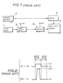
- FIG.1 shows an essential part of an example of a conventional bipolar PROM.
- the bipolar PROM generally comprises an address input circuit 2, a memory cell array 3, a programming power source circuit 4, a write circuit 5, and a decoder 6.
- a write mode a predetermined memory cell within the memory cell array 3 is selected by an address which is received from an address driver (writer) 1 via the address input circuit 2 and the decoder 6.
- the write-in of data to the predetermined memory cell is made via the write circuit 5 which is driven by the programming power source circuit 4.
- a power source voltage Vcc is set to 7 V as shown in FIG.2(A) and a write voltage Vw from the programming power source circuit 4 is set to 20 V as shown in FIG.2(B), for example.
- the power source voltage Vcc is set to 5 V as shown in FIG.2(A) and the write voltage Vw from the programming power source circuit 4 is set to 0 V.
- the power source voltage Vcc during the write mode is set greater than that during the read mode because in the write mode there is a need to supply a large current to the selected memory cell so as to break and short-circuit a junction of the selected memory cell.
- the memory cell array 3 of the bipolar PROM usually employs the TTL.
- the address input circuit 2 is TTL circuit and a PROM writer which programs the bipolar PROM is designed to operate with the TTL level.
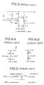
- FIG.3 shows an example of the TTL address input circuit 2.
- the TTL address input circuit 2 comprises transistors Tr1 through Tr4, resistors r1 through r3, and a diode d which are connected as shown.
- Vcc denotes the power source voltage and GND denotes the ground voltage.
- CMOS circuit for the address input circuit 2 because a low power consumption and a high-speed operation can be realized and there is study to employ the CMOS circuit for the address input circuit 2.
- problems occur since the input threshold value of the CMOS circuit changes when the power source voltage Vcc changes and the PROM writer is designed to operate with the TTL level.
- the input threshold value Vth is set to an intermediate voltage between the power source voltage Vcc and the ground. For example, this intermediate voltage is approximately Vcc/2. For this reason, the input threshold value Vth of the CMOS address input circuit 2 changes when the power source voltage Vcc changes.
- FIG.4B shows an equivalent circuit of the CMOS address input circuit 2.
- the CMOS address input circuit 2 is illustrated as a series connection of two variable resistors Ra and Rb the resistances of which vary depending on the input voltage.
- the input threshold value Vth of the CMOS address input circuit 2 can be set to approximately 1.4 V in the read mode but the input threshold value Vth increases to approximately 2.1 V when the power source voltage Vcc is increased in the write mode.
- a low logic level is 0.8 V or less and a high logic level is 2.0 V or greater and the PROM writer is designed with this typical TTL level.
- the CMOS address input circuit 2 regards this input voltage as a low logic level since it is less than the input threshold value Vth as shown in FIG.5.
- the CMOS address input circuit 2 carries out an erroneous operation in the write mode in response to the input voltage which is set in conformance with the TTL level.
- the PROM writer which operates with the TTL level cannot be used when the CMOS address input circuit 2 is used because the TTL level cannot be discriminated correctly in the write mode.
- the input threshold value of the CMOS address input circuit 2 is reduced in the write mode to enable a correct discrimination of the high and low logic levels in conformance with the TTL, it then becomes impossible to correctly discriminate the high and low logic levels in the read mode. For this reason, there is a problem in that the PROM writer must be designed to operate with the CMOS level if the CMOS address input circuit 2 is to be used.
- the existing PROM writers are already designed to operate with the TTL level, it would be extremely troublesome and expensive to design new PROM writers exclusively for the CMOS address input circuit 2 to make the same programming as the existing PROM writers.
- Another and more specific object of the present invention is to provide a programmable semiconductor memory circuit comprising a memory cell array having memory cells, a write circuit which is driven by a first power source voltage only in a write mode for writing data into the memory cells of the memory cell array, an address input circuit which is driven by a second power source voltage for supplying an address signal to the memory cell array, where the second power source voltage has a voltage higher in the write mode than in a read mode and the address input circuit has an arrangement such that an input threshold value thereof changes when the second power source voltage changes, and an input level correcting circuit supplied with the first power source voltage only in the write mode for supplying the first power source voltage to the address input circuit to pull up a signal level at an input of the address input circuit in the write mode so that a signal having a high logic level at the input of the address input circuit is greater than the input threshold value of the address input circuit.
- the correct operation of the address input circuit is ensured even when the address input circuit is made of a CMOS or BiCMOS circuit to realize a low power consumption and a high speed operation, and the existing PROM writer can be used as it is without the need of a new PROM writer designed exclusively for the CMOS or BiCMOS address input circuit.
- FIG.6 generally shows a programmable semiconductor memory circuit according to the present invention for explaining an operating principle thereof.
- the write circuit 5 is driven by the write power source voltage Vw from a programming power source circuit (not shown) only during the write mode.
- An address input circuit 15 is driven by the power source voltage Vcc which is higher in the write mode than in the read mode and supplies an address signal to the memory cell array 3 via a decoder 18.
- the address input circuit 15 is made of a CMOS or BiCMOS circuit.
- An input level correcting circuit 16 is coupled between a line of the write power source voltage Vw and a line of the address signal.
- the write power source voltage Vw is supplied to the address input circuit 15 only in the write mode.
- the input threshold value of the address input circuit 15 increases due to the change in the power source voltage Vcc, but the input signal level of the address input circuit 15 is pulled up by the write power source voltage Vw to make up for the insufficient input signal level with respect to the increased input threshold value of the address input circuit 15. Accordingly, even when the input threshold value of the address input circuit 15 increases in the write mode, it is possible to correctly drive the address input circuit 15 with the TTL level and the existing PROM writer can be used as it is for the programming. In other words, there is no need to design a new PROM writer exclusively for the address input circuit 15 which is a CMOS or BiCMOS circuit.
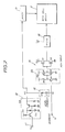
- FIG.7 shows an essential part of an embodiment of the programmable semiconductor memory circuit according to the present invention.
- the address input circuit 15 shown in FIG.7 is a CMOS circuit comprising a circuit part 60, a p-channel MOS transistor Q1 and an n-channel MOS transistor Q2 which are connected in series between the power source voltage Vcc and the ground.
- the circuit part 60 comprises transistors Q11 through Q13 and a resistor R11 which are connected as shown. But it is of course possible to use other arrangements for the address input circuit 15 such as an embodiment shown in FIG.8.
- the address input circuit 15 is a BiCMOS circuit comprising the circuit part 60, a p-channel MOS transistor Q3 and an n-channel MOS transistor Q4 which are connected in series between the power source voltage Vcc and the ground, two npn transistors Q5 and Q6 which are connected in series between the power source voltage Vcc and the ground, and resistors R1 and R2 which are connected as shown.
- the write power source voltage Vw is applied to a programming terminal 11 and is supplied to a switching circuit 12.
- the write power source voltage Vw is also used to generate a chip enable signal which is supplied to an output buffer (not shown) as will be described later.
- the switching circuit 12 is turned ON when the supplied write power source voltage Vw exceeds a voltage which is determined by a threshold voltage of a Zener diode D Z1 . In other words, the switching circuit 12 is turned ON only in the write mode when the write power source voltage Vw is 20 V as shown in FIG.2(B). When the switching circuit 12 is ON, the write power source voltage Vw is supplied to the write circuit 5.
- the input level correcting circuit 16 comprises a resistor R and a diode D which are connected in series between nodes N1 and N2.
- the node N1 connects the address input circuit 15 and the input level correcting circuit 16 to a terminal 17 which receives the address signal.
- the node N2 connects the switching circuit 12 and the write circuit 5.
- the power source voltage Vcc supplied to the address input circuit 15 is increased to 7 V as shown in FIG.2(A).
- a predetermined memory cell within the memory cell array 3 is selected by the address signal which is received from the terminal 17 via the address input circuit 15 and the decoder 18.
- the write power source voltage Vw which is 20 V as shown in FIG.2(B) is supplied to the write circuit 5 via the programming terminal 11 and the switching circuit 12. The data is written into the predetermined memory cell by the operation of the write circuit 5.
- the input threshold value of the address input circuit 15 increases to 2.3 V, for example.
- the write power source voltage Vw from the switching circuit 12 is supplied to the address input circuit 15 via the input level correcting circuit 16 in the write mode so as to pull up the level of the signal at the input of the address input circuit 15 and make up for the increase in the input threshold value.
- the level of the signal which has a high logic level at the input of the address input circuit 15 is pulled up to such a level that it is correctly discriminated as a high logic level in the address input circuit 15 which has the increased input threshold value in the write mode.
- the level of the signal which has a low logic level at the input of the address input circuit 15 is maintained lower than the input threshold value thereof even when the pull up takes place. Accordingly, even when the input threshold value of the address input circuit 15 becomes 2.3 V, for example, the signal level at the input of the address input circuit 15 is pulled up to a sufficiently high level so that the high logic level in conformance with the TTL is pulled up to a value greater than 2.3 V at the input of the address input circuit 15. As a result, a correct operation of the address input circuit 15 is ensured and it is possible to use the existing PROM writer which operates with the TTL level as it is.
- the power source voltage Vcc supplied to the address input circuit 15 is set to 5 V as shown in FIG.2(A).
- a predetermined memory cell within the memory cell array 3 is selected by the address signal which is received from the terminal 17 via the address input circuit 15 and the decoder 18.
- the write power source voltage Vw which is 0 V as shown in FIG.2(B) is supplied to the switching circuit 12 and the switching circuit 12 is OFF.
- the voltage which is supplied to the address input circuit 15 via the input level correcting circuit 16 is 0 V and the signal level within the address input circuit 15 returns to the normal CMOS level.
- the data is read out from the predetermined memory cell by operating a read circuit (not shown) which will be described later.
- the input level correcting circuit 16 is not limited to that shown in FIG.7, but it is of course possible to use other arrangements for the input level correcting circuit 16 such as an embodiment shown in FIG.9.
- the input level correcting circuit 16 comprises in addition to the resistor R and the diode D a Zener diode D Z2 which is connected as shown.
- the Zener diode D Z2 clamps the high level signal to a predetermined value to prevent an excessively large voltage from being supplied to the address input circuit 15.
- FIGS.10A and 10B are diagrams for explaining the operation of the above described embodiment.
- FIG.10A shows the high and low voltage levels at the input (node N1) of the address input circuit 15 in the TTL read mode. In this state, the potential at the node N2 is 0 V and the input level correcting circuit 16 is inactive.
- FIG.10B shows the limit of the high and low voltage levels at the input (node N1) of the address input circuit 15 in the write mode. In this state, the potential at the node N2 is 20 V and the input level correcting circuit 16 is active.
- the input threshold value Vth of the address input circuit 15 rises to 2.3 V but the potential at the node N1 also rises as indicated by the solid line in FIG. 10B. That is, the low voltage level remains at 0.8 V but the high voltage level rises to 2.9 V, and the input threshold value Vth is always set to an intermediate value between the high and low voltage levels.
- FIG.11 shows the embodiment in more detail.
- the programmable semiconductor memory circuit comprises the memory cell array 3, the write circuit 5, X and Y address buffers 51 and 52, the decoder 18, the switching circuit 12, the input level correcting circuit 16, a chip enable signal generator 53, a sense amplifier 54, and an output buffer 55.
- the address input circuit 15 is provided within the address buffers 51 and 52.
- the basic construction of this memory circuit is known as a programmable read only memory (PROM).
- the decoder 18 selects one word line responsive to a signal received from the X-address buffer 51.
- the write circuit 5 selects one bit line responsive to a signal received from the Y-address buffer 52.
- the sense amplifier 54 selects one bit line responsive to the signal received from the Y-address buffer 52.
- the output buffer 55 outputs data read out from a selected memory cell of the memory cell array 3 when enabled by a chip enable signal CE.
- This chip enable signal CE is output from the chip enable signal generator 53 which generates the chip enable signal CE from the write power source voltage Vw ( CE ).
- the address buffers 51 and 52 select a memory cell of the memory cell array 3 via the decoder 18 and the write circuit 5. In addition, a write current is applied to the selected memory cell from a terminal 56 via the write circuit 5.
- the address buffers 51 and 52 select a memory cell of the memory cell array 3 via the decoder 18 and the sense amplifier 54.
- the data read out from the selected memory cell is output from the terminal 56 via the sense amplifier 54 and the output buffer 55.
Landscapes
- Read Only Memory (AREA)
Applications Claiming Priority (2)
| Application Number | Priority Date | Filing Date | Title |
|---|---|---|---|
| JP21606388 | 1988-08-30 | ||
| JP216063/88 | 1988-08-30 |
Publications (2)
| Publication Number | Publication Date |
|---|---|
| EP0357502A2 true EP0357502A2 (fr) | 1990-03-07 |
| EP0357502A3 EP0357502A3 (fr) | 1992-01-02 |
Family
ID=16682695
Family Applications (1)
| Application Number | Title | Priority Date | Filing Date |
|---|---|---|---|
| EP19890402355 Withdrawn EP0357502A3 (fr) | 1988-08-30 | 1989-08-29 | Circuit de mémoire programmable à semi-conducteurs |
Country Status (3)
| Country | Link |
|---|---|
| US (1) | US4972375A (fr) |
| EP (1) | EP0357502A3 (fr) |
| KR (1) | KR930002385B1 (fr) |
Families Citing this family (7)
| Publication number | Priority date | Publication date | Assignee | Title |
|---|---|---|---|---|
| JP3228759B2 (ja) * | 1990-01-24 | 2001-11-12 | セイコーエプソン株式会社 | 半導体記憶装置及びデータ処理装置 |
| US5103425A (en) * | 1991-03-11 | 1992-04-07 | Motorola, Inc. | Zener regulated programming circuit for a nonvolatile memory |
| JPH05128866A (ja) * | 1991-10-31 | 1993-05-25 | Toshiba Corp | ランダムアクセスメモリの書き込み、読出し制御回路 |
| IL100598A0 (en) * | 1992-01-06 | 1992-09-06 | Univ Bar Ilan | Dataflow computer |
| JPH05307616A (ja) * | 1992-04-30 | 1993-11-19 | Hitachi Ltd | 半導体装置 |
| JP2905666B2 (ja) * | 1992-05-25 | 1999-06-14 | 三菱電機株式会社 | 半導体装置における内部電圧発生回路および不揮発性半導体記憶装置 |
| JP5888387B1 (ja) * | 2014-10-22 | 2016-03-22 | ミツミ電機株式会社 | 電池保護回路及び電池保護装置、並びに電池パック |
Family Cites Families (5)
| Publication number | Priority date | Publication date | Assignee | Title |
|---|---|---|---|---|
| JPS5891680A (ja) * | 1981-11-26 | 1983-05-31 | Fujitsu Ltd | 半導体装置 |
| JPS5922295A (ja) * | 1982-06-30 | 1984-02-04 | Fujitsu Ltd | 半導体記憶装置 |
| US4734885A (en) * | 1985-10-17 | 1988-03-29 | Harris Corporation | Programming arrangement for programmable devices |
| US4901280A (en) * | 1986-07-11 | 1990-02-13 | Texas Instruments Incorporated | Pull-up circuit for high impedance word lines |
| FR2609831B1 (fr) * | 1987-01-16 | 1989-03-31 | Thomson Semiconducteurs | Circuit de lecture pour memoire |
-
1989
- 1989-08-24 US US07/397,838 patent/US4972375A/en not_active Expired - Fee Related
- 1989-08-24 KR KR8912076A patent/KR930002385B1/ko not_active Expired - Fee Related
- 1989-08-29 EP EP19890402355 patent/EP0357502A3/fr not_active Withdrawn
Also Published As
| Publication number | Publication date |
|---|---|
| KR930002385B1 (en) | 1993-03-29 |
| KR900003901A (ko) | 1990-03-27 |
| EP0357502A3 (fr) | 1992-01-02 |
| US4972375A (en) | 1990-11-20 |
Similar Documents
| Publication | Publication Date | Title |
|---|---|---|
| EP0317430B1 (fr) | Circuit logique utilisant des semi-conducteurs bipolaires et MOS complémentaires ainsi qu'une mémoire employant ledit circuit | |
| EP0639000B1 (fr) | Circuit amplificateur du type bascule | |
| KR970001345B1 (ko) | 레벨 쉬프터 | |
| US4984207A (en) | Semiconductor memory device | |
| US4972375A (en) | Programmable semiconductor memory circuit | |
| US5587952A (en) | Dynamic random access memory including read preamplifiers activated before rewrite amplifiers | |
| US4424582A (en) | Semiconductor memory device | |
| JPS5856286B2 (ja) | 出力バッファ回路 | |
| JPH0439158B2 (fr) | ||
| EP0368328B1 (fr) | Circuit de détection de transition d'adresse | |
| KR0147712B1 (ko) | 에스램의 저전압 동작용 비트 라인 회로 | |
| US5281873A (en) | Sense amplifier control circuit | |
| JPS582437B2 (ja) | スリ−ステイト出力回路 | |
| KR0161307B1 (ko) | 반도체 메모리 장치 | |
| EP0469834B1 (fr) | Circuit logique BICMOS avec immunité à l'auto-survoltage et méthode adaptée | |
| EP0508652B1 (fr) | Circuit de mémoire à semi-conducteurs | |
| EP0443776A2 (fr) | Circuit de détection pour dispositif de mémoire non volatile | |
| US4815036A (en) | Programmable logic array having an on/off sense function | |
| US5267216A (en) | BICMOS local address transition detection circuit | |
| US4242605A (en) | Transient array drive for bipolar ROM/PROM | |
| US5963077A (en) | Auto mode selector | |
| US5535166A (en) | Circuit for isolating and driving interconnect lines | |
| US5130637A (en) | Constant voltage generating circuit | |
| EP0424249A2 (fr) | Circuit générateur d'impulsions de déclenchement | |
| JP2972960B2 (ja) | デジタル出力回路 |
Legal Events
| Date | Code | Title | Description |
|---|---|---|---|
| PUAI | Public reference made under article 153(3) epc to a published international application that has entered the european phase |
Free format text: ORIGINAL CODE: 0009012 |
|
| AK | Designated contracting states |
Kind code of ref document: A2 Designated state(s): DE FR GB |
|
| PUAL | Search report despatched |
Free format text: ORIGINAL CODE: 0009013 |
|
| AK | Designated contracting states |
Kind code of ref document: A3 Designated state(s): DE FR GB |
|
| 17P | Request for examination filed |
Effective date: 19920624 |
|
| 17Q | First examination report despatched |
Effective date: 19930506 |
|
| STAA | Information on the status of an ep patent application or granted ep patent |
Free format text: STATUS: THE APPLICATION IS DEEMED TO BE WITHDRAWN |
|
| 18D | Application deemed to be withdrawn |
Effective date: 19930917 |